Article

Near-Field Light-Bending Photonic Switch: Physics of Switching Based on Three-Dimensional Poynting Vector Analysis

1
School of Computer Science and Electronic Engineering, Bangor University, Dean Street, Bangor, Gwynedd LL57 1UT, UK
2
School of Physics and Optoelectronic Engineering, Xidian University, No. 2 South Taibai Road, Xi’an 710071, Shaanxi Province, China
3
V. E. Zuev Institute of Atmospheric Optics, Siberian Branch, Russian Academy of Sciences, 1 Zuev Square, 634021 Tomsk, Russia
4
Nondestructive Testing School, Tomsk Polytechnic University, 36 Lenin Avenue, 634050 Tomsk, Russia
*
Author to whom correspondence should be addressed.
Photonics 2022, 9(3), 154; https://doi.org/10.3390/photonics9030154
Submission received: 29 January 2022 / Revised: 23 February 2022 / Accepted: 3 March 2022 / Published: 4 March 2022
(This article belongs to the Special Issue Photonic Jet: Science and Application)

Abstract

:
Photonic hook is a high-intensity, bent light focus with a proportional curvature to the wavelength of the incident light. Based on this unique light-bending phenomenon, a novel near-field photonic switch by means of a right-trapezoid dielectric Janus particle-lens embedded in the core of a planar waveguide is proposed for switching the photonic signals at two common optical communication wavelengths, 1310 nm and 1550 nm, by using numerical simulations. The signals at these two wavelengths can be guided to different routes according to their oppositely bent photonic hooks to realise wavelength selective switching. The switching mechanism is analysed by an in-house developed three-dimensional (3D) Poynting vector visualisation technology. It demonstrates that the 3D distribution and number of Poynting vector vortexes produced by the particle highly affect the shapes and bending directions of the photonic hooks causing the near-field switching, and multiple independent high-magnitude areas matched by the regional Poynting vector streamlines can form these photonic hooks. The corresponding mechanism can only be represented by 3D Poynting vector distributions and is being reported for the first time.

1. Introduction

Switch is the most basic component to make, break, or divert the connection from one conductor to another in a circuit. The conventional electronic switch is a solid-state mechanical device, though the sensors can be used to automate it in certain working environments. The concept of the switch can be used for signal processing and other applications of modern communication technologies, and activation/deactivation of signals and data routing are the major functions of a switch, sometimes called logic signal switch, in here [1]. With the development of data technology and mobile computing, the optical signal in the form of light replaced the electronic signal to become the mainstream method of data transmission with the aid of optical fibres [2,3]. For this reason, a photonic switch is developed to control the light (optical signals) propagation with high efficiency, and its switching time is much faster than that of a conventional electronic switch, due to the unparalleled speed of light [4,5]. In this field, wavelength switching is a technology used in optical communication to select individual wavelengths of light and forward the selected input light to the separate paths for specific data routing [6]. Meanwhile, many optical fibres are optimised for the optical signals at wavelengths of 1310 nm and 1550 nm due to their lower losses in the glass fibre [7]. Wavelength division multiplexing (WDM) and Dense WDM (DWDM) are the technologies that enable a number of separate optical signals with different wavelengths to be transmitted in an optical fibre [8,9], but the sizes of these devices limit their applications for the future photonic integrated circuits and lab-on-a-chip devices. As an alternative, the planar dielectric waveguide, in the form of a dielectric film (core) sandwiched between cladding layers, better applies to these integrated optoelectronic devices due to a relatively simple and compact structure and the consequent production advantages [10,11]. Theoretically, the optical signal can be fast and accurately transmitted in the core of a planar waveguide relying on the total internal reflection occurring at the interface between the core and cladding [12].
In this paper, a novel all-dielectric photonic switch is realised by the near-field light-bending effect of photonic hook which is a curved and localised, high-intensity light beam focused by a dielectric micro-particle [13]. When it was invented, it was the only other instance of artificially bent light apart from the Airy beam [13,14]. Meanwhile, it is highly related to the concept of photonic jet or can be directly understood as a photonic jet asymmetrically shifting in optical phase due to difference in phase velocity caused by regional refractive-index contrast. Typically, it is produced by the light focusing through a dielectric right-trapezoid Janus microparticle with the asymmetry in geometrical shape and internal refractive index from its prism end [14,15,16]. This wavefront curvature normally appears in the shadow direction of the particle and significantly influence the electric field distribution in that area. Minin et al. experimentally generated a photonic hook in terahertz (THz) band for the first time using a relatively simple experimental setup, meanwhile proving the proportional relationship between the wavelength of incident light and curvature of photonic hook [15]. Based on this finding, Geints et al. raised the proofs-of-concept of similar photonic switches, and herein, photonic hooks could function like switching channels after passing several differently configurated dielectric particles, such as the flipped prism, Janus bar, and off-axis Fresnel zone plate [17]. Moreover, most photonic hooks are graphically represented by the distributions of electric field and Poynting vector on the median section. This two-dimensional (2D) plot is sufficient to characterise the complete shape and curvature of a photonic hook; however, it is difficult to analyse the light-bending process and the physics behind the phenomenon because the influence of the photonic energy that flows into the median section from other planes cannot be quantified, even visualised [18]. Yue et al. developed a 3D mapping technology to track the power flow (Poynting vectors) of a photonic jet focused by a spherical mesoscale micro-particle, and the circulation and convergence of 3D Poynting vectors inside the dielectric particle were demonstrated for the first time [19]. The same technology is used in this study to solve the above issue.
In this article, we propose a novel photonic hook light-bending optical switch by means of a conventional right-trapezoid-shaped dielectric particle embedded in the core of a planar waveguide. The operation of signal switching at two communication wavelengths, λ = 1310 and 1550 nm, are numerically simulated. Its setup and operating wavelengths are designed for the applications of optical communication and are different from those in [17]. The separation of switching channels for the signals at these two wavelengths is demonstrated by the overall distribution of the electric field and profiles of the generated photonic hooks. The corresponding simulation data is analysed by 3D Poynting vector visualisation technology to deeply investigate the physics and mechanism of switching.

2. Results and Discussion

2.1. Concept and Modelling

The numerical model of the proposed photonic switch is built in the commercial finite integral technique (FIT) software package, CST Microwave Studio (CST), which is widely used for design and analysis of nanophotonic devices [19,20]. A right-trapezoid-shaped particle with the refractive index of n = 2, which can be possibly constituted by the dielectric materials with the similar refractive index, e.g., Boron nitride (BN), MICROPOSIT® S1800 photoresist (S1800), etc. (n ranges 1.9–2.1 in near-infrared band depending on thickness and structure), is implanted in the facet of the quartz core of a planar waveguide with n = 1.44 [21,22,23]. The difference of the refractive indexes for the particle material at the wavelengths of 1310 nm and 1550 nm is neglected to simplify and standardise the models for comparison purposes. The assumed planar waveguide is able to ideally approximate the plane wave propagation and eliminate the interference for the transmitted light at wavelengths of 1310 nm and 1550 nm, and the implanted particle with a small relative dimension to the core (d/D ≤ 0.08, where d and D are the particle size and thickness of the core of the planar waveguide, respectively) [24,25]. The sketch of this design is shown in Figure 1a I and the diagrams of Figure 1a II and III illustrate the effect of a trapezoid particle switching the incident lights with short and long wavelengths which are 1310 nm and 1550 nm in this case. As a discussion of the proof of concept, the proposed photonic hook switch could be fabricated using the technologies of plano-convex-microsphere (PCM) lens laser nano-marking and two-photon polymerization (TPP) 3D printing (resolution of fs laser wavelength) with two example materials—BN and S1800, respectively—aided by the integrated high-precision piezo positioning stages and femtosecond (fs) lasers (positioning resolution of the stage: 1 nm; minimum corner radius of the structure: ~100 nm) [26,27]. A PCM lens is a dielectric lens made up of a high-index microsphere integrated with a plano-convex lens, which can deliver a high patterning resolution that is smaller than the diffraction limit for a precision machining of the facet of the planar waveguide core in a trapezoid shape by a fs laser [26]. TPP 3D printing is an additive fabrication technology to create micro/nano features relying on the photoresist solidification only occurring at the fs laser focus [27]. It can in situ fill the micro/nanosized photonic wires of dielectric material layer by layer in the cavity created by PCM lens marking technology with a high degree of design freedom.
For the simulation setup in CST, the core material with the refractive index of n = 1.44 is used to encapsulate the trapezoid particle as long as the flat end facing the background medium of air (n = 1) with the open boundary condition (effect of Perfectly matched layers, PML) along with x, y, and z directions to simulate the planar waveguide transmission and photonic hook switching in the air. The incident plane wave is y-polarized and propagates along z axis with the amplitude of 1 v/m. The trapezoid particle is placed as the prism encountering the light in z direction. The short base, long base, height, thickness, and prism angles of the trapezoid are 2.79 µm, 3.72 µm, 2.79 µm, 2.79 µm, and 71.57° in this design, respectively. Furthermore, the frequency domain solver and tetrahedral meshing with the average edge length of 188 nm (min. and max. edge lengths are 33 nm and 339 nm, respectively; the approximate level of λ/7) are used in the model for adaptive refinement of the simulation accuracy with the autonomous adjustment of mesh sizes on the surfaces and edges of the geometries. The modelling diagram is shown in Figure 1b. The data of the Poynting vector in the modelling space generated by CST is exported and then independently processed by a MATLAB® programme to plot the contour of the Poynting vector magnitudes in a certain plane and a full 3D distribution of the Poynting vector streamlines entering the particle.

2.2. Switching and 2D Distributions

The dielectric particle in the proposed photonic switch design is individually irradiated by the plane-wave lights (optical signals) at wavelengths of 1310 nm and 1550 nm, and Figure 2 shows the corresponding distributions of the squared total magnitudes of electric field ( E 2 , E is electric field) and real part of complex Poynting vectors and their directions (unit: V·A/m2) [28]. The distributions of E 2 field in Figure 2a,b demonstrate a clear separation of switching paths. In Figure 2a, the wavefront of 1310 nm light develops in a route approaching the side of the trapezoid long base, which forms a downward photonic hook. By contrast, the development of the photonic hook at the wavelength of 1550 nm is different from that for 1310-nm-wavelength light. It propagates in an almost straight path with a slightly upward curvature in the middle. The optical signals with the same wavelengths should be switched to the routes in accordance with the photonic hook curvatures, and the distance between two routes in the shadow area of the particle can provide the dimensional tolerance for the device fabrication. Theoretically, two ports can be set up in the middle of the photonic hook routes to separately receive the corresponding signals.
Figure 2c,d demonstrate the 2D Poynting vector distributions on the median section for the models irradiated by the optical signals with wavelengths of 1310 nm and 1550 nm, respectively. The asymmetric vortexes of Poynting vector streamlines are shown in the dielectric particles in both figures. It is known that the photonic energy is able to flow in and out through these vortexes representing the singularities of Poynting vectors possibly associated with topological charge [29,30,31]. Consequently, the layout of these vortexes can influence the flow direction and intensity of Poynting vectors, especially in the areas which are close to the particle boundaries. In Figure 2c for 1310 nm optical signal, the prism of the dielectric particle leads the difference of phase velocity in the particle and generates four vortexes at the output end of the particle, marked as v1, v2, v3, and v4 in the figure. Referring to the contour and flows of Poynting vectors in Figure 2c, it is shown that two saddle points, outward spiral v1 and inward spiral v2, are in high-intensity and low-intensity areas, respectively. This means that the photonic power flow passes into the median plane at v1 position in the upper half of the particle, meanwhile exiting the plane at v2 position in the lower half. The corresponding power flow exchange and influences of vortexes v3 and v4 around the output area of the particle make the flows of Poynting vectors in the generated photonic hook downward in general. However, it is noted that the photonic hook of 1310-nm-wavelength irradiation is divided into two high-magnitude areas (marked as a1 and a2) by a Poynting vector flow represented by a pink arrow in Figure 2c. This separation is unusual and rare in the discovered photonic hooks and different from the photonic hook in Figure 2a for the squared electric field distribution. Rather than the downward photonic hook for the optical signal of 1310 nm wavelength, a slightly upward photonic hook is created by the same trapezoid particle for the incidence of 1550-nm-wavelength light. Two outward vortexes, v5 and v6 in Figure 2d, shape the flow distribution and produce two narrow low-magnitude regions compressing the high-magnitude area of the photonic hook in the middle.

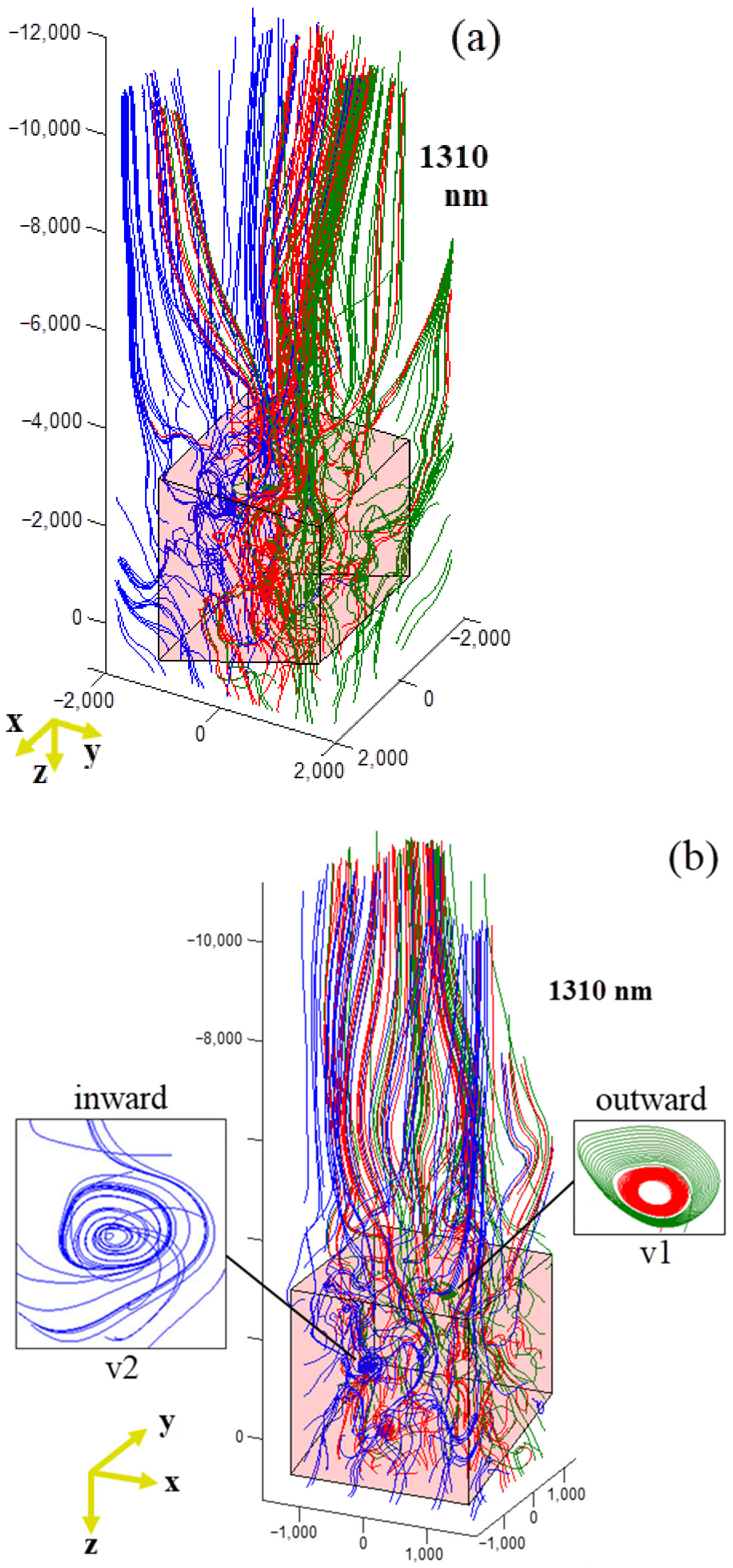
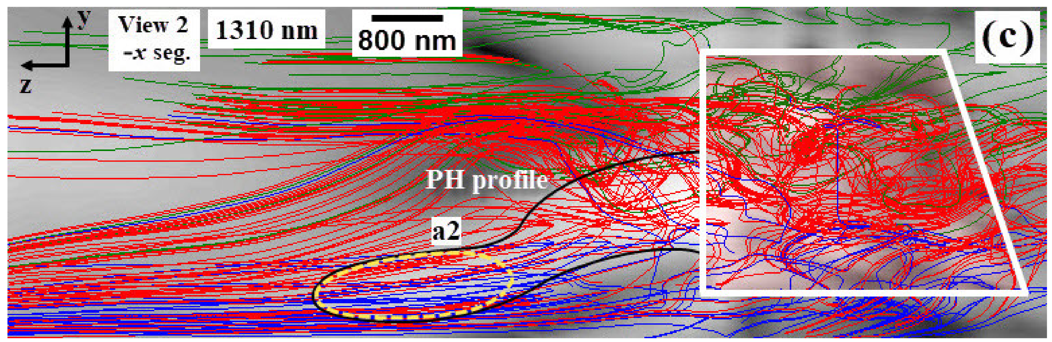
2.3. 3D Poynting Vector Analysis

The physical mechanism behind the switching of the optical signals at wavelengths of 1310 nm and 1550 nm and their field distributions in Figure 2 is further investigated by the 3D Poynting vector visualisation analysis [19]. Compared to 2D analysis, 3D analysis will provide additional information on light flows between different cross sections and also the root of formation of optical vortexes and other singular points. All Poynting vectors entering the dielectric particle from the prism end are tracked and then visualised by an in-house developed MATLAB® programme. Due to a large amount of Poynting vector data imported in the programme, the plotted Poynting vector streamlines are marked in different colours to indicate the regions where they are tracked in the model. The colour codes are distributed along the y axis to equally divide the whole modelling space into three sections: the blue lines for the long-base section (−y direction), red lines for the middle section (around 0 position on the y axis), and green lines for the short-base section (+y direction). An overview of the 3D Poynting vector distribution for the model of 1310-nm-wavelength irradiation is shown in Figure 3a. All Poynting vector streamlines flow upwards from the prism end to the flat facet of the particle (vector arrows are hidden due to a high density of streamlines); however, the presented features of 3D distribution are significantly different from those in the 2D format shown in Figure 2. The Poynting vector streamlines can continuously and freely develop in multiple directions and finally create a tangled-roots-like structure. Figure 3b as a close-up view of the same model demonstrates the locations of the vortexes with the insets of two important ones, v1 and v2, also indicated in Figure 2. Except for the different spin directions of v1 and v2 shown in Figure 2, 3D visualisation of Poynting vectors can graphically represent the orientations of v1 and v2 and fully indicate this difference in Figure 3b. It is shown that the centre and spin-orbit of v1 is approximately perpendicular to the z axis and faces upward in -z direction, meanwhile, the same features are generally in the direction of 45° to the x axis for v2. In addition, the inner and outer circles of v1 are in red and green, respectively, which means the photonic energy can flow to the middle and upper parts of the particle and modelling space through this vortex using multiple routes.
The proposed switch enables the selection of the propagation routes for the optical signals at wavelengths of 1310 nm and 1550 nm, as shown in Figure 2, due to the opposite bending directions of photonic hooks. This phenomenon is unusual for two electromagnetic irradiations with such a small wavelength gap in the field of photonic hook study. This is mainly attributed to the separation of two high-magnitude areas of Poynting vectors as a1 and a2 shown in Figure 2c for the irradiation at the wavelength of 1310 nm. The corresponding contour seems to not perfectly match with the flow direction and density of Poynting vectors in 2D Poynting vector distribution (Figure 2c), especially for the gap between a1 and a2. Nevertheless, it can be properly explained by 3D Poynting vector analysis in this case. Here we use a 2D Poynting vector distribution of the median yz plane (x = 0) in greyscale as a screen to divide the 3D Poynting vector visualisation model for the 1310-nm-wavelength irradiation into +x segment and −x segment, as shown in the diagram in Figure 4a. View 1 (+x segment visible) and view 2 (−x segment visible) are defined as two observation angles to separately represent two segments of 3D Poynting vector distributions without allowing perspective in such a setup, as shown in Figure 4b,c. In these two figures, the profiles of the downward photonic hook and the high-magnitude areas, a1 and a2, are portrayed by black solid lines and yellow dashed lines, respectively. It is found that the profiles of a1 and a2 high-magnitude areas can be sequentially matched by the dense Poynting vector streamlines in the regions where are close to the median yz plane of x = 0 in +x segment (view 1) and −x segment (view 2), respectively. The gap between a1 and a2 shown in Figure 2c is attributed to this collective effect, and it leads to the unique downward photonic hook jointed by two high-magnitude areas for the irradiation at the wavelength of 1310 nm and spatially ensures optical isolation with the photonic hook (switching route) of 1550-nm-wavelength signal.
Figure 5a,b illustrate the overview and close-up views of 3D Poynting vector distribution for the model of 1550-nm-wavelength irradiation. Compared to the distributions for the model of 1310-nm-wavelength irradiation shown in Figure 3, the Poynting vector streamlines in Figure 5 are less swirling in the trapezoid particle and more straight in the volume of the generated photonic hook, which reflects a smaller number of vortexes shown in Figure 5. Two key vortexes, v5 and v6, are indicated in Figure 5 as well. The photonic hook of the irradiation at a longer wavelength of 1550 nm appears in the region with the maximum density of Poynting vector streamlines, basically filling the central volume of the modelling space. These features are in accordance with the 2D Poynting distribution on the median yz plane for the same model shown in Figure 2d, which induces an almost straight, slightly upward photonic hook. Therefore, it is noted that the difference of spatial location of Poynting vector vortexes crucially influence the bending direction of the generated photonic hook and vary the subsequent propagation routes for the lights (optical signals) with similar wavelengths. This effect can be only represented by 3D Poynting vector distributions [32] and cause multiple localised high-magnitude regions of Poynting vectors to constitute a complete single photonic hook.

3. Conclusions

The numerical simulation proves that the proposed near-field light-bending photonic switch as a Janus right-trapezoid-shaped dielectric particle embedded in the core facet of a planar waveguide can successfully switch and guide the optical signals at two common communication wavelengths, 1310 nm and 1550 nm, to different propagation routes based on photonic hook phenomenon. The opposite bending directions are found for the generated photonic hooks; the downward one for 1310-nm-wavelength irradiation is, unusually, separated into two high-magnitude areas by a Poynting vector flow. Three-dimensional Poynting vector analysis demonstrates that the corresponding high-magnitude areas can be sequentially matched by the Poynting vector streamlines in segments, which means that photonic hook can exist in a similar joining form. The corresponding mechanism is reported for the first time, and the future plan of the authors is to visualise similar 3D Poynting vector flows using virtual reality (VR) technology.

Author Contributions

Conceptualization, L.Y., O.V.M. and I.V.M.; methodology, L.Y.; software, L.Y., Z.W., and B.Y.; validation, Z.W. and O.V.M.; formal analysis, L.Y.; investigation, L.Y., O.V.M. and I.V.M.; resources, Y.X. and Y.E.G.; data curation, L.Y.; writing—original draft preparation, L.Y.; writing—review and editing, Z.W., O.V.M. and I.V.M.; visualization, L.Y.; supervision, L.Y., Z.W., O.V.M. and I.V.M.; project administration, L.Y., Z.W., O.V.M. and I.V.M.; funding acquisition, L.Y., Z.W., O.V.M. and I.V.M. All authors have read and agreed to the published version of the manuscript.

Funding

This research was funded by the Welsh European Funding Office (WEFO), European ERDF grants, grant number CPE 81400 and SPARCII c81133, the Royal Society International Exchanges Cost Share Scheme UK, grant number IEC\R2\202040, the Russian Foundation for Basic Research, grant number 21-57-10001, and the Tomsk Polytechnic University Development Program.

Institutional Review Board Statement

Not applicable.

Informed Consent Statement

Not applicable.

Data Availability Statement

This study did not report any data.

Conflicts of Interest

The authors declare no conflict of interest.

References

  1. Jaeger, R.C. Microelectronic Circuit Design; McGraw-Hill: New York, NY, USA, 1997. [Google Scholar]
  2. Rao, M.M. Optical Communication; Universities Press: Hyderabad, India, 2001. [Google Scholar]
  3. Senior, J.M.; Jamro, M.Y. Optical Fiber Communications; Pearson/Prentice Hall: Hoboken, NJ, USA, 2009. [Google Scholar]
  4. Jin, C.Y.; Wada, O. Photonic switching devices based on semiconductor nano-structures. J. Phys. D Appl. Phys. 2014, 47, 133001. [Google Scholar] [CrossRef] [Green Version]
  5. Testa, F.; Pavesi, L. Optical Switching in Next Generation Data Centers; Springer: Beilin, Germany, 2017. [Google Scholar]
  6. Bernstein, G.M.; Lee, Y.; Galver, A.; Martensson, J. Modeling WDM Wavelength Switching Systems for Use in GMPLS and Automated Path Computation. IEEE/OSA J. Opt. Commun. Netw. 2009, 1, 187–195. [Google Scholar] [CrossRef]
  7. Cancellieri, G. Single-Mode Optical Fibres; Elsevier Science: Amsterdam, The Netherlands, 2014. [Google Scholar]
  8. Ozcelik, D.; Parks, J.W.; Wall, T.A.; Stott, M.A.; Cai, H.; Parks, J.W.; Hawkins, A.R.; Schmidt, H. Optofluidic wavelength division multiplexing for single-virus detection. Proc. Natl. Acad. Sci. USA 2015, 112, 12933–12937. [Google Scholar] [CrossRef] [Green Version]
  9. Sadot, D.; Boimovich, E. Tunable optical filters for dense WDM networks. IEEE Commun. Mag. 1998, 36, 50–55. [Google Scholar] [CrossRef]
  10. Ramo, S.; Whinnery, J.R.; van Duzer, T. Fields and Waves in Communications Electronics; John Wiley and Sons: Hoboken, NJ, USA, 1984. [Google Scholar]
  11. Prajzler, V.; Nekvindova, P.; Lyutakov, O. Flexible polymer planar optical waveguides. Radioengineering 2014, 23, 776–782. [Google Scholar]
  12. Polky, J.N.; Mitchell, G.L. Metal-clad planar dielectric waveguide for integrated optics. J. Opt. Soc. Am. 1974, 64, 274–279. [Google Scholar] [CrossRef]
  13. Minin, I.V.; Minin, O.V. Diffractive Optics and Nanophotonics: Resolution below the Diffraction Limit; Springer: Berlin, Germany, 2016. [Google Scholar]
  14. Yue, L.; Minin, O.V.; Wang, Z.; Monks, J.N.; Snalin, A.S.; Minin, I.V. Photonic hook: A new curved light beam. Opt. Lett. 2018, 43, 771–774. [Google Scholar] [CrossRef] [PubMed]
  15. Minin, I.V.; Minin, O.V.; Katyba, G.M.; Chernomyrdin, N.V.; Kurlov, V.N.; Zaytsev, K.I.; Yue, L.; Wang, Z.; Christodoulides, D.N. Experimental observation of a photonic hook. Appl. Phys. Lett. 2019, 114, 031105. [Google Scholar] [CrossRef]
  16. Minin, I.V.; Minin, O.V.; Glinskiy, I.A.; Khalilubin, R.A.; Malureanu, R.; Lavrinenko, A.; Yakubovsky, D.I.; Volcow, V.S.; Ponomarev, D.S. Experimental verification of a plasmonic hook in a dielectric Janus particle. Appl. Phys. Lett. 2021, 118, 131107. [Google Scholar] [CrossRef]
  17. Geints, Y.E.; Minin, O.V.; Yue, L.; Minin, I.V. Wavelength-Scale Photonic Space Switch Proof-of-Concept Based on Photonic Hook Effect. Ann. Phys. 2021, 553, 2100192. [Google Scholar] [CrossRef]
  18. Soukoulis, C.M.; Wegener, M. Past achievements and future challenges in the development of three-dimensional photonic metamaterials. Nat. Photonics 2011, 5, 523–530. [Google Scholar] [CrossRef] [Green Version]
  19. Yue, L.; Yan, B.; Monks, J.N.; Dhama, R.; Jiang, C.; Minin, O.V.; Minin, I.V.; Wang, Z. Full three-dimensional Poynting vector flow analysis of great field-intensity enhancement in specifically sized spherical-particles. Sci. Rep. 2019, 9, 20224. [Google Scholar] [CrossRef] [PubMed] [Green Version]
  20. Yue, L.; Yan, B.; Wang, Z.B. Photonic nanojet of cylindrical metalens assembled by hexagonally arranged nanofibers for breaking the diffraction limit. Opt. Lett. 2016, 41, 1336–1339. [Google Scholar] [CrossRef] [PubMed]
  21. Lee, S.Y.; Jeong, T.Y.; Jung, S.; Yee, K.J. Refractive Index Dispersion of Hexagonal Boron Nitride in the Visible and Near-Infrared. Phys. Status Solidi B 2018, 256, 1800417. [Google Scholar] [CrossRef]
  22. Tan, C.Z. Determination of refractive index of silica glass for infrared wavelengths by IR spectroscopy. J. Non-Cryst. Solids 1998, 223, 158–163. [Google Scholar] [CrossRef]
  23. MICROPOSIT® S1800® Photoresist Datasheet. Available online: https://amolf.nl/wp-content/uploads/2016/09/datasheets_S1800.pdf (accessed on 25 January 2022).
  24. Elson, J.M. Propagation in planar waveguides and the effects of wall roughness. Opt. Express 2001, 9, 461–475. [Google Scholar] [CrossRef]
  25. Gomez-Correa, J.E.; Balderas-Mata, S.E.; Garza-Rivera, A.; Jaimes-Najera, A.; Trevino, J.P.; Coello, V.; Rogel-Salazar, J.; Chavez-Cerda, S. Mathematical-Physics of propagating modes in planar waveguides. Rev. Mex. F’ısica E 2019, 65, 218–222. [Google Scholar] [CrossRef] [Green Version]
  26. Yan, B.; Yue, L.; Monks, J.N.; Yang, X.; Xiong, D.; Jiang, C.; Wang, Z. Superlensing plano-convex-microsphere (PCM) lens for direct laser nano-marking and beyond. Opt. Lett. 2020, 45, 1168–1171. [Google Scholar] [CrossRef]
  27. Dietrich, P.I.; Blaicher, M.; Reuter, I.; Billah, M.; Hoose, T.; Hofmann, A.; Caer, C.; Dangel, R.; Offrein, B.; Troppenz, U.; et al. In situ 3D nanoprinting of free-form coupling elements for hybrid photonic integration. Nat. Photon. 2018, 12, 241–247. [Google Scholar] [CrossRef]
  28. Stratton, J.A. Electromagnetic Theory, 1st ed.; McGraw-Hill: New York, NY, USA, 1941. [Google Scholar]
  29. Bohren, C.F.; Huffman, D.R. Absorption and Scattering of Light by Small Particles; Wiley: Hoboken, NJ, USA, 1983. [Google Scholar]
  30. Wang, Z.B.; Luk’yanchuk, B.S.; Hong, M.H.; Lin, Y.; Chong, T.C. Energy flow around a small particle investigated by classical Mie theory. Phys. Rev. B 2004, 70, 035418. [Google Scholar] [CrossRef]
  31. Kumar, V.; Viswanathan, N.K. Topological structures in the Poynting vector field: An experimental realization. Opt. Lett. 2013, 38, 3886–3889. [Google Scholar] [CrossRef] [PubMed]
  32. Minin, O.V.; Minin, I.V. Optical Phenomena in Mesoscale Dielectric Particles. Photonics 2021, 8, 591. [Google Scholar] [CrossRef]
Figure 1. (a) I, diagram of photonic switch design; II and III, principle of the proposed photonic switching at two different wavelengths (b) CST modelling diagram.
Photonics 09 00154 g001aPhotonics 09 00154 g001b
Figure 2. The distributions of the squared total magnitude of electric field ( E 2 ) for the irradiations with wavelengths of 1310 nm (a) and 1550 nm (b). Two-dimensional Poynting vector distributions for the irradiations with wavelengths of 1310 nm (c) and 1550 nm (d). The dimensions of the trapezoid particle are short base, 2.79 µm; long base, 3.72 µm; height, 2.79 µm; thickness, 2.79 µm; and prism angle, 71.57°.
Photonics 09 00154 g002
Figure 3. Overview (a) and the rotated view (b) of 3D Poynting vector distribution for the model of 1310 nm irradiation with the colour codes of streamlines: blue lines for long-base section (−y direction), red lines for middle section (around 0 position on y axis), and green lines for short-base section (+y direction). Insets in (b): Outward vortex v1 and Inward vortex v2.
Photonics 09 00154 g003
Figure 4. (a) Diagram of view 1 and view 2 segments and 3D Poynting vector distributions for (b) view 1 +x segment and (c) view 2 −x segment of the model with the irradiation at the wavelength of 1310 nm. Orientations of the particle in Figure 4b,c are reversed due to the change of frames of references for the observers in view 1 and view 2 as shown in Figure 4a.
Photonics 09 00154 g004aPhotonics 09 00154 g004b
Figure 5. Overview (a) and the rotated view (b) of 3D Poynting vector distribution for the model of 1550 nm irradiation with the colour codes of streamlines: blue lines for long-base section (−y direction), red lines for middle section (around 0 position on y axis), and green lines for short-base section (+y direction).
Photonics 09 00154 g005
Publisher’s Note: MDPI stays neutral with regard to jurisdictional claims in published maps and institutional affiliations.

