Article

All-Optical Phase-Change Memory with Improved Performance by Plasmonic Effect

Faculty of Electrical Engineering and Computer Science, Key Laboratory of Photoelectric Materials and Devices of Zhejiang Province, Ningbo University, Ningbo 315211, China
*
Author to whom correspondence should be addressed.
Photonics 2022, 9(3), 132; https://doi.org/10.3390/photonics9030132
Submission received: 13 January 2022 / Revised: 15 February 2022 / Accepted: 16 February 2022 / Published: 25 February 2022
(This article belongs to the Topic Optical and Optoelectronic Materials and Applications)

Abstract

:
The combination of the integrated waveguide and phase-change materials (PCMs) provides a promising platform for reconfigurable and multifunctional photoelectric devices. Through plasmonic enhancement and the low loss propagation of the waveguide, the footprint and power consumption of the photoelectric device can be effectively improved. In this work, a metal double-ring structure embedded with phase change materials was proposed to utilize the plasmonic effect for enhancement of the light-matter interaction. In particular, the overall temperature difference in the PCM cell can be confined within 2 °C during the crystallization process, thus avoiding the interior heterogeneous crystallization. The insertion loss of the cell in amorphous and crystalline states at a wavelength of 1550 nm are 2.3 dB and 1.0 dB, respectively. A signal contrast ratio of 15.8% is achieved under the ultra-small footprint (50 × 90 nm2) at a wavelength of 1550 nm.

1. Introduction

Photonic integrated circuits have become more and more attractive because they not only increase information transmission rates and bandwidth, but also overcome the shortcomings of traditional electronic integrated circuits that are time-consuming and energy-inefficient [1,2]. The photonic integrated platform based on phase-change materials (PCMs) has been proposed for reconfigurable and non-volatile devices due to the huge optical contrast between the amorphous and crystalline states of the PCMs [3]. PCMs are widely used in integrated photonic switches [4,5], optical phase shifters [6] and meta-surface fields [7] due to their non-volatile and reconfigurable properties. The intensity or phase of propagating light can be modulated by the change in crystalline fraction, paving the way for photonic multi-level storages [8], neural morphology [9], and in-memory computing [10]. Farmakidis et al. [11] recently demonstrated a nonvolatile integrated electro-optic device with a combination of PCM and nano-plasmonic which enables the multilevel states both by optical and electrical programming. The modulation depth among multilevel states can be further improved by using a gold nanoring photonic modulator to selectively absorb the spectrum [12]. A faster switching speed and lower energy consumption can be achieved by a type of plasmonic dimer nanoantenna embedded with PCM on top of an integrated waveguide due to the plasmonic enhancement [13]. Different from building phase-change memory devices on top of silicon nitride waveguides, planar photonic crystal nanocavities are photonic crystals etched into a silicon film consisting of bottom and top symmetrical layers of low-nitrogen material helping to improve the optical nonlinearity and mechanical stability [14,15]. For operation at a telecommunication wavelength of 1550 nm, combining integrated photonics with nanoscale plasmonics, allows for both low-loss light delivery and strong light-matter interaction in a compact footprint [16,17]. Combining plasmons with PCM can reduce the size of the device to tens of nanometers or even less—significantly below the diffraction limit of conventional optical devices, useful optical contrast and low IL silicon photonic waveguide devices can be obtained [11,18]. In such optical memory cells using integrated phase-change photonic devices, switching is the basic operation of a storage device [13]. Information storage is accomplished by propagating light pulses along the waveguide to reversibly switch the state of the PCMs. However, these studies on integrated photonic devices have not been considered the uniform heating distribution which influences the operation reliability as a result of the heterogeneous crystallization in the PCM.

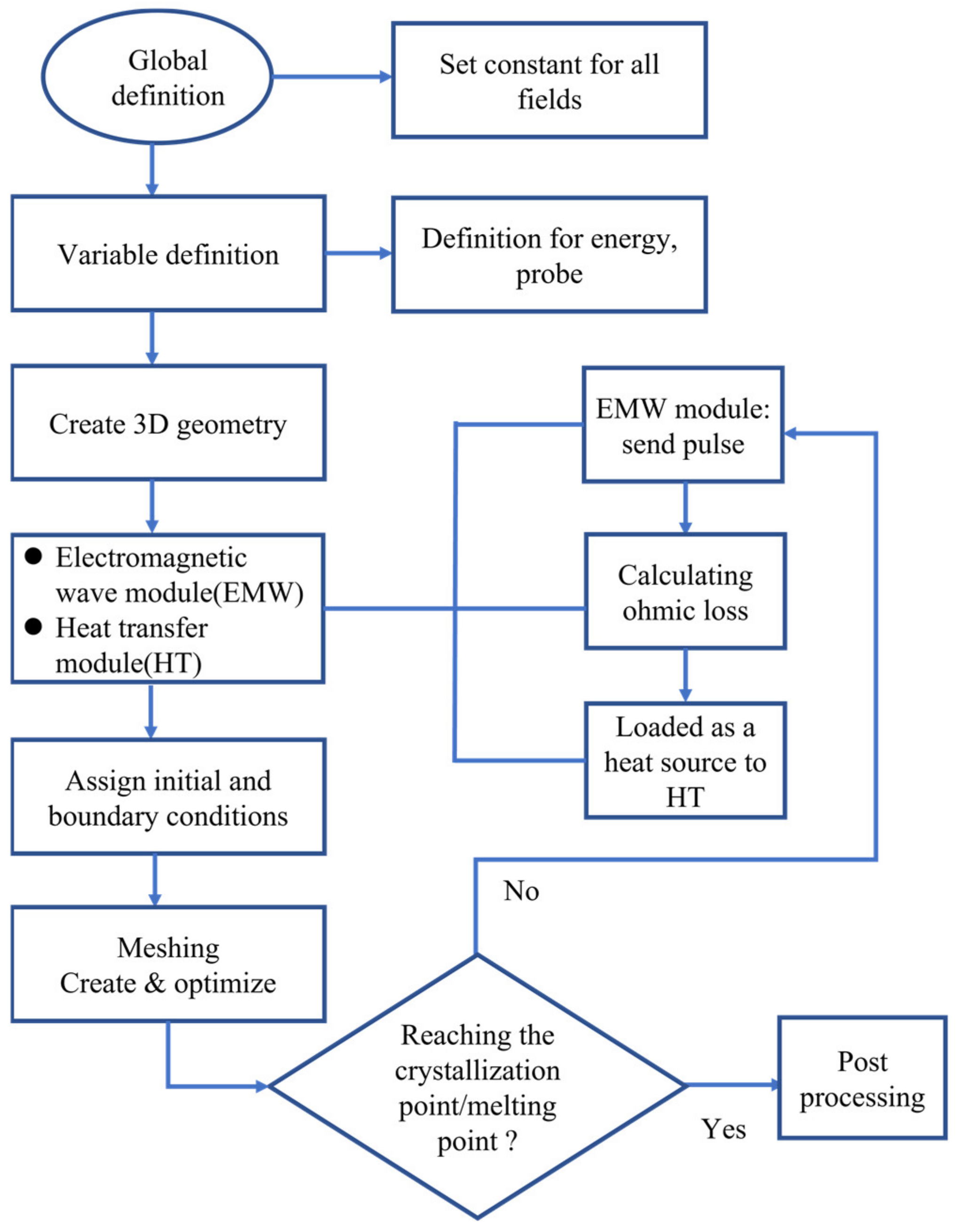
2. Materials and Methods

In this work, a metal nanoantenna is combined with photonic integrated circuits to enhance the light-matter interaction between phase-change materials and propagating waveguide modes. The generation of plasma originates from the excitation of conduction electrons at the interface between the metal and the dielectric surface. Plasma takes advantage of the coupling of light to charges like electrons in metals and allows breaking the diffraction limit for the localization of light into subwavelength dimensions enabling strong field enhancements [19]. In our structure, the plasma is induced by a double-ring-metal nanoantenna embedded in the integrated waveguide, and PCM is sandwiched between two metal rings to reduce the footprint of the devices. Such hybrid structure generates resonance between the metals to enhance the electromagnetic field in the nano-gap, thereby reducing power consumption. The high refractive index of the waveguide confines light to the diffraction-limited optical mode. The plasmonic structure couples the propagation mode into the nano-gap, greatly enhancing the coupling efficiency and increasing the amplitude of the confined field. What’s more, the whole PCM can be evenly heated by such a hybrid structure to realize phase transition under an optical pulse, which can avoid interior heterogeneous crystallization.
As shown in Figure 1a, the nanoantenna hybrid structure with a concentric circle-like shape is placed on Si3N4 strip waveguide, fixing the PCMs between metals to produce a nano-gap enhanced plasmonic effect. In detail, the device consists of Si3N4 rib waveguide (1300 nm × 170 nm) fabricated on top of a 2 um thick SiO2 substrate [20], the radius Ag nano-disk, the width of GST, and width of Ag nanoring are 25, 20 and 65 nm, respectively. Such a device geometry can achieve maximum field enhancement effect, thereby reducing power consumption and increasing switching speed. Silver is employed in this structure due to its excellent plasmonic properties in the near-infrared band [21]. However, attention must be paid to the diffusion effect of metal ions, which will cause changes in the optical properties of the chalcogenide compound [22]. Therefore, it is necessary to add a corresponding barrier layer such as silicon nitride and titanium nitride to avoid this phenomenon [23]. Writing/erasing operations can be performed by triggering phase transition between amorphous and crystalline states of PCM, here we used the well-studied Ge2Sb2Te5 (GST) as the PCM due to its significant variation of complex refractive index, good thermal stability, high switching speed, large number of achievable rewrite cycles [24]. Silver plasmonic nanostructures and GST are deposited in the center of the waveguide. The different amount of light absorption by GST leads to the change in transmission serving as reading the stored data for this photonic device. The fundamental mode TE0 at a wavelength of 1550 nm is supported to transmit in the Si3N4 strip waveguide. The nanoantenna hybrid structure has three different positions along with the depth of waveguide such as none-embedded, half-embedded, and full-embedded in the waveguide, as shown in Figure 1b–d. The required power consumption and insertion loss are compared for these devices in the following sections.
The geometry of the hybrid structure including the radius of inner Ag nano-disc, the widths of both outer Ag and GST nano-rings and the thickness of this whole structure is required to optimize so that GST is located at the maximum field enhancement. Simulations are carried out using finite element modeling in the software package COMSOL to solve the following phenomenon: light propagation across the integrated device, thermal diffusion caused by light energy absorption and the phase transition induced by the consequent increase in temperature [20]. The heating process of PCM under pulse stimulation was simulated by coupling the electromagnetic wave and heat transfer module. The optical model is solved in COMSOL, using the RF (radio frequency) module. A second-order boundary scattering condition was applied to the outer surface to avoid any nonphysical reflections. The source port and listener port are located on the surface perpendicular to the waveguide and other surfaces are provided with perfect electric conductor conditions. Heat diffusion calculations are carried out using the COMSOL HT (heat transfer) module. The bottom surface of SiO2 and waveguide surfaces perpendicular to the waveguide axis are fixed at room temperature, while all other surfaces are considered adiabatic. To eliminate the thermal boundary resistance effect, we set the thermal boundary resistance for the GST domain (TBR = 3 × 10⁻⁸ m2K/W [25]), the Si3N4-Ag interface (TBR = 5 × 10⁻⁹ m2K/W [26]), and Si3N4-SiO2 interface (TBR = 1 × 10⁻⁹ m2K/W [27]). A pulse of light is emitted from the port, and the Ag and phase-change material absorb heat, completing the write and erase operations. The heat source in the heat transfer module is coupled with the electromagnetic wave module. The coupling partial differential equation of the heat transfer module and the electromagnetic wave module is:
ρ C P u T = ( K T ) + J E ,
where ρ is the density, Cp is the heat capacity at constant pressure, u is the velocity of the charge-carriers, K and T are the thermal conductivity and temperature, J and E are current density and electric field, respectively. The coupling of the heat transfer module and the electromagnetic field module is realized by solving partial differential equation. The flow chart of COMSOL calculation steps is shown in Figure 2. Table 1 gives the various material parameters used in our simulation.
When light is incident on the interface between metal and dielectric, free electrons on the metal surface collectively oscillate. The electromagnetic waves couple with free electrons on the metal surface to form a near-field electromagnetic wave that propagates along the metal surface. Thus, the electromagnetic field is limited in this small gap through resonance, and the interaction between GST and the transmitted light is enhanced. The most significant factors influencing the plasmonic behavior is the size of the structure [20]. The strength of the interaction is controlled by the thickness of the metal layer [40].
To explore the maximum field enhancement effect of a plasmonic metal nanoantenna, the electric field distribution was simulated firstly for the device without GST. The field enhancement factor (EF) is usually used as a physical quantity to evaluate the electric field enhancement effect. The definition method of EF is defined as [13], EF = |ELOC/E0|, where ELOC and E0 are the electric field norm evaluated within the nanogap and input electric field, respectively. The relationship among EF, radius, and width of the Ag ring is shown in Figure 3a. The EF reaches a maximum when the radius Ag nano-disk and width of Ag nanoring are 25 and 65 nm, respectively. With fixed the inner and outer metal dimensions, the width of GST and thickness of the whole structure also directly affect the electric field, as shown in Figure 3b. To obtain a strong field enhancement effect, the width and thickness of GST are optimized to be 20 nm and 30 nm, respectively. With such geometry of the device structure, the phase transition of GST can be triggered by the strong plasmonically-enhanced resonant mode. The optimized structure enables the formation of hybridized plasmonic resonance. It is reasonable that the hybridized plasmonic resonance results in the highest EM field for the optimized structure. It can be deduced that there are two hybridized modes: bonding and antibonding modes [41]. In the bonding mode, the currents move in different directions, so the electric field is scattered outside the Ag ring. Anti-bonding mode corresponds to the same direction movement of the carriers, which causes the electric field to concentrate in the optimized structure enabling the highest EM field enhancement. The optimized double-nanoring structure is used for the subsequent simulations and studies. In Figure 3c,d, we show how transmission, reflection, and scattering in the waveguide vary with metallic disc and ring. The transmission T through the waveguide basically follows the EF radius dependence, with the slope in the transmission roughly coinciding with the peak in the EF. The mismatch between the EF and T peak positions originates from the interference between the plasmonic resonance modes and the propagating waves [13].

3. Results and Discussion

3.1. Memory Performance

Phase transition of GST sandwiched between Ag nano-disc and nanoring will cause a drastic change in the local refractive index, and consequently the transmission of the device varies. First, we simulate the transmittance, reflection, and insertion loss of the device when the phase change material is completely crystalline and amorphous. These results simulate the read operation, performed by sending a low power optical pulse (which does not induce any significant heating) down the waveguide. The device usually has a lower transmission in the crystalline state due to its larger absorption coefficient in comparison with that in the amorphous state. However, it is noted that the transmission in the crystalline state is gradually higher than that of the amorphous state at a wavelength larger than 1440 nm, as shown in Figure 4a. This is the result of coupling modulation between the nanogap and the waveguide, where an increase in wavelength-dependent refractive index leads to an increase in coupling with the plasma mode within the nanogap [11].
The insertion loss (IL) of the phase change device is defined as:
IL = 10 log 10 P out P in
here, Pin and Pout are defined as the input power and output power, respectively. As shown in Figure 4b, the overall insertion loss of the device is less than 4 dB. In the crystalline state, the insertion loss increases slowly with wavelength, while in the amorphous state, the insertion loss increases from 0.5 to 4 dB. The decrease in device transmittance indicates an increase in insertion loss. This trend is consistent with Figure 4a. Due to the generation of more plasmons, the phase matching will be impeded, and the coupling efficiency will decrease, resulting in higher insertion loss in the amorphous state [42]. Figure 4c,d show electric field diagrams in amorphous and crystalline states, respectively. It can be seen that the nanogap electric field in the amorphous state is much higher than that in the crystalline state, and consequently the total energy absorbed increases significantly, so the transmittance is lower than that of the crystalline state. The readout signal contrast is defined as T am T cry T am , when T cry > T am , as T cry T am T cry , the contrast reached 15.8% at the wavelength of 1550 nm, compared with Ref [13], the contrast is improved by 3%.
The optical properties including transition and IL were obtained for the devices with half-embedded and full-embedded nanoantenna structures (see Figure 1b,c). The corresponding results are listed in Table 2. The embedded junction has a slight increase in insertion loss. This is due to the strong interaction between the plasmon resonance mode and the electromagnetic field resonance in the waveguide mode [43]. Compared with half-embedded and full-embedded nanoantenna structures at a wavelength of 1550 nm, the non-embedded one has a larger optical contrast. The propagating light experiences reflection and scattering due to the introduction of interface among the metal, the waveguide, and PCM for the embedded structure. When PCM is in crystalline state, the reflection and scattering will be stronger due to the existence of much more free carriers. Therefore, the transmittance in crystalline state decreases more than that in amorphous state for the embedded structure. That is why the optical contrast will decrease with the increase of the embedded depth. Active tuning of the antenna resonance position can be achieved by ultrafast laser pulse pumping, and ultrafast optical switches or tunable filters based on this embedded structure [44].

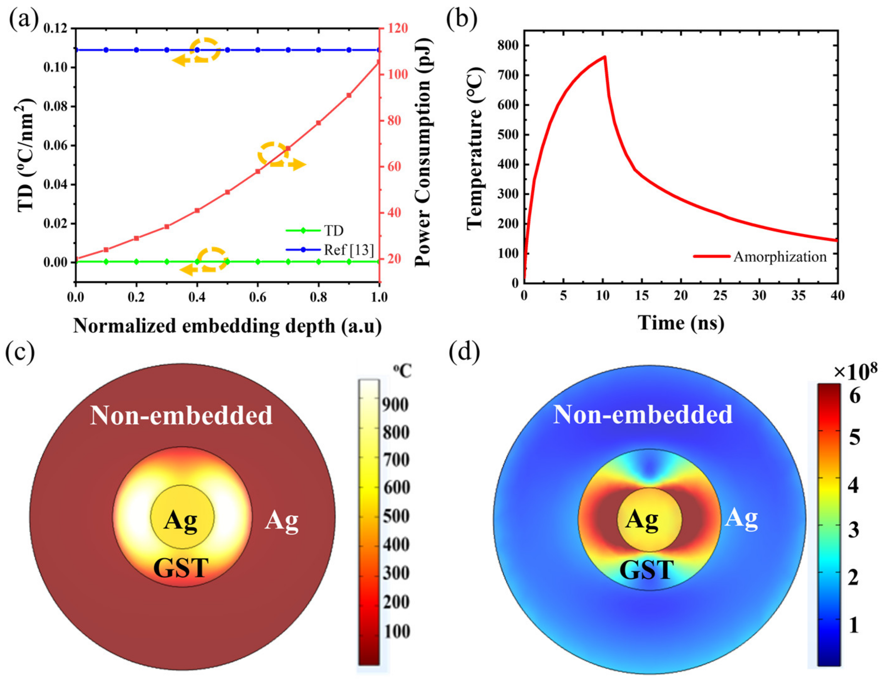
3.2. Crystallization and Amorphization Process

When such a structure is used as a non-volatile memory, the intensity and width of the pulses required to complete writing/erasing operations determine the power consumption of the device. For writing operation, pulses with higher power and shorter duration are used to couple into the waveguide, so that the phase change material is rapidly heated up and reaches above the melting point. Then it is quenched to be in the amorphous state. For erasing operation, it is difficult to use a single pulse excitation, because the absorption rate increases significantly in the crystalline state. In most studies, two-step pulses are used [45,46]. A short and relatively high-power pulse is followed by a long and low-power second pulse to achieve the erase operation.
A rectangular pulse with a power of 20 mW and a duration of 1 ns was employed to send into the waveguide so that GST reaches above the crystallization temperature to complete amorphous-to-crystalline transition. The entire GST area is heated uniformly for all studied structures (see Figure 5a–c), suggesting that the crystallization of PCM is characterized as the homogenous mode. The electric field enhancement is the largest in the gap of non-embedded structure (see Figure 5d–f), thereby reducing power consumption and increasing switching speed. Thanks to the small size in the nanostructure, it will cause rapid temperature diffusion, resulting in uniform changes in temperature (see Figure 5g). Figure 5h shows the transient temperature distribution during crystallization. After reflection and scattering for the embedded devices, the propagating light with lower energy would have a weaker interaction with PCM, which leads to a small absorption of light. It leads to a smaller Joule heating and lower average temperature. Therefore, the average temperature is much higher for the non-embedded device compared to the other two embedded devices. In Figure 5e, the electric field intensity for erasing operation is 104 times higher than that for readout. Such high plasmonic effect in the nano-gap is helpful for the reduction in power consumption.
The temperature difference (TD) of the device is defined as:
TD = T max T min S ,
where Tmax, Tmin represent the maximum and minimum temperature on the heated surface, respectively. S represents the heated area. TD changes little with increasing embedding depth for the studied structure (see Figure 6a). Compared with [13], the value of TD is much smaller because the whole phase transition region is uniformly heated. Such uniform heat distribution in PCM helps to reduce the power loss caused by partial crystallization and to be more reliable to realize multi-level storage.
Figure 6a shows the minimum pulse energy required to complete writing operation for different embedded depth. The energy consumption increases with the increase of the embedded depth. This is because when the waveguide is embedded in a high refractive index medium, the scattered light will interfere with the transmitted light, thereby reducing the light transmission in the embedded waveguide [43]. We apply a 1.8 mW, 10 ns pulse to induce phase change for the non-embedded device (see Figure 6b). It is shown that the optical pulse is able to complete the amorphization process. The temperature in most areas of GST exceeds its melting point during the amorphization process (see Figure 6c). The transient electric field distribution at this time is shown in Figure 6d, which is very consistent with the temperature distribution in Figure 6c.
The enhancement of the light-matter interaction between the PCM and the propagating waveguide mode is favorable to reducing power consumption in-memory applications. We compared several different types of devices in terms of the energy required for crystallization and amorphization (see Table 3).
The optical pulses with widths as short as 1 ns and 11 ns were employed to complete the write and erase process, respectively, suggesting the high-speed characteristics. It also can be seen from the thermal transient distribution that the conversion speed is much higher than that of traditional phase change memory devices [45,46].

4. Conclusions

In summary, we combine plasma with photonic integrated circuits, which greatly increases the interaction of light and matter in the integrated phase-change photonic memory cell. The heating distribution of the phase change zone in such a structure demonstrates uniformity during the erasing/writing process. The overall temperature difference of the GST is well confined to a small value. The maximum temperature difference does not exceed 2 °C during crystallization process, which is conducive to the uniform turnover of the PCMs. The device achieves 15.8% optical contrast under the ultra-small footprint at 1550 nm, and low insertion loss of crystalline and amorphous states, which are 2.3 and 1.0 dB, respectively. The devices based on the plasmonic structures demonstrate high optical contrast and low power consumption. The results provide a general approach to develop reconfigurable and multifunctional photoelectric devices with the ultra-compact footprint, fast switching speed, and low power.
Though the performance improvement comes at the expense of increased manufacturing complexity, such plasmonic devices can be fabricated by lithographic processes. In our future work, for example, the waveguide will be fabricated by electron-beam lithography (EBL) on a 330 nm-thick Si3N4 wafter with 2 μm-thick SiO2 film on a Si wafer. A second lithography will be carried out to determine the double-ring pattern. Silver will then be deposited via electron beam evaporation. Finally, the PCM will be deposited by magnetron sputtering and patterned by EBL using lift-off.

Author Contributions

Conceptualization, Y.Z. and L.M.; methodology, W.S.; software, W.S.; validation, Y.L. and W.S.; formal analysis, W.S.; investigation, Y.L.; resources, Y.L.; data curation, W.S.; writing—original draft preparation, W.S.; writing—review and editing, W.S. and Y.L.; visualization, W.S. and Y.L.; supervision, Y.L.; project administration, Y.L.; funding acquisition, Y.L. All authors have read and agreed to the published version of the manuscript.

Funding

This work was supported by the National Natural Science Foundation of China (Grant No. 61874062), Zhejiang Provincial Natural Scientific Foundation of China (Grant No. LR22F040002), and Ningbo Municipal Natural Science Foundation of China (Grant No. 202003N4012).

Institutional Review Board Statement

Not applicable.

Informed Consent Statement

Not applicable.

Data Availability Statement

The data presented in this study are available in insert article here.

Conflicts of Interest

The authors declare no conflict of interest.

References

  1. Wu, C.; Yu, H.; Lee, S.; Peng, R.; Takeuchi, I.; Li, M. Programmable phase-change metasurfaces on waveguides for multimode photonic convolutional neural network. Nat. Commun. 2021, 12, 96. [Google Scholar] [CrossRef] [PubMed]
  2. Feldmann, J.; Youngblood, N.; Li, X.; Wright, C.D.; Bhaskaran, H.; Pernice, W.H.P. Integrated 256 Cell Photonic Phase-Change Memory With 512-Bit Capacity. IEEE J. Sel. Top. Quantum Electron. 2020, 26, 1–7. [Google Scholar] [CrossRef] [Green Version]
  3. Wang, J.; Wang, L.; Liu, J. Overview of Phase-Change Materials Based Photonic Devices. IEEE Access 2020, 8, 121211–121245. [Google Scholar] [CrossRef]
  4. Zheng, J.; Fang, Z.; Wu, C.; Zhu, S.; Xu, P.; Doylend, J.K.; Deshmukh, S.; Pop, E.; Dunham, S.; Li, M.; et al. Nonvolatile Electrically Reconfigurable Integrated Photonic Switch Enabled by a Silicon PIN Diode Heater. Adv. Mater. 2020, 32, e2001218. [Google Scholar] [CrossRef]
  5. Ríos, C.; Zhang, Y.; Shalaginov, M.Y.; Deckoff-Jones, S.; Wang, H.; An, S.; Zhang, H.; Kang, M.; Richardson, K.A.; Roberts, C.; et al. Multi-Level Electro-Thermal Switching of Optical Phase-Change Materials Using Graphene. Adv. Photonics Res. 2021, 2, 2000034. [Google Scholar] [CrossRef]
  6. Taghinejad, H.; Abdollahramezani, S.; Eftekhar, A.A.; Fan, T.; Hosseinnia, A.H.; Hemmatyar, O.; Dorche, A.E.; Gallmon, A.; Adibi, A. ITO-Based Microheaters for Reversible Multi-Stage Switching of Phase-Change Materials: Towards Miniaturized Beyond-Binary Reconfigurable Integrated Photonics. Opt. Express 2020, 29, 20449–20462. [Google Scholar] [CrossRef]
  7. Abdollahramezani, S.; Hemmatyar, O.; Taghinejad, H.; Krasnok, A.; Kiarashinejad, Y.; Zandehshahvar, M.; Alù, A.; Adibi, A. Tunable nanophotonics enabled by chalcogenide phase-change materials. Nanophotonics 2020, 9, 1189–1241. [Google Scholar] [CrossRef]
  8. Zhu, M.; Song, W.; Konze, P.M.; Li, T.; Gault, B.; Chen, X.; Shen, J.; Lv, S.; Song, Z.; Wuttig, M.; et al. Direct atomic insight into the role of dopants in phase-change materials. Nat. Commun. 2019, 10, 3525. [Google Scholar] [CrossRef] [Green Version]
  9. Cheng, Z.; Ríos, C.; Pernice, W.; Wright, C.; Bhaskaran, H.J.S.A. On-chip photonic synapse. Sci. Adv. 2017, 3, e1700160. [Google Scholar] [CrossRef] [Green Version]
  10. Ríos, C.; Youngblood, N.; Cheng, Z.; Gallo, M.L.; Pernice, W.; Wright, C.; Sebastian, A.; Bhaskaran, H.J.S.A. In-memory computing on a photonic platform. Sci. Adv. 2019, 5, eaau5759. [Google Scholar] [CrossRef] [Green Version]
  11. Farmakidis, N.; Youngblood, N.; Li, X.; Tan, J.; Swett, J.; Cheng, Z.; Wright, C.D.; Pernice, W.H.P.; Bhaskaran, H.J.S.A. Plasmonic nanogap enhanced phase-change devices with dual electrical-optical functionality. Sci. Adv. 2019, 5, eaaw2687. [Google Scholar] [CrossRef] [Green Version]
  12. Singh, M.; Raghuwanshi, S.; Srinivas, T. Nanophotonic on-chip hybrid plasmonic electro-optic modulator with phase change materials. Phys. Lett. A 2019, 383, 3196–3199. [Google Scholar] [CrossRef]
  13. Gemo, E.; Carrillo, S.G.; De Galarreta, C.R.; Baldycheva, A.; Hayat, H.; Youngblood, N.; Bhaskaran, H.; Pernice, W.H.P.; Wright, C.D. Plasmonically-enhanced all-optical integrated phase-change memory. Opt. Express 2019, 27, 24724–24737. [Google Scholar] [CrossRef]
  14. Kassa-Baghdouche, L.; Boumaza, T.; Bouchemat, M. Optimization of Q-factor in nonlinear planar photonic crystal nanocavity incorporating hybrid silicon/polymer material. Phys. Scr. 2015, 90, 065504. [Google Scholar] [CrossRef]
  15. Kassa-Baghdouche, L.; Boumaza, T.; Bouchemat, M. Planar photonic crystal nanocavities with symmetric cladding layers for integrated optics. Opt. Eng. 2014, 53, 127107. [Google Scholar] [CrossRef]
  16. Chen, C.; Mohr, D.A.; Choi, H.-K.; Yoo, D.; Li, M.; Oh, S.-H. Waveguide-Integrated Compact Plasmonic Resonators for On-Chip Mid-Infrared Laser Spectroscopy. Nano Lett. 2018, 18, 7601–7608. [Google Scholar] [CrossRef]
  17. Shen, J.; Jia, S.; Shi, N.; Ge, Q.; Gotoh, T.; Lv, S.-L.; Liu, Q.; Dronskowski, R.; Elliott, S.R.; Song, Z.; et al. Elemental electrical switch enabling phase segregation-free operation. Science 2021, 374, 1390–1394. [Google Scholar] [CrossRef]
  18. Gemo, E.; Faneca, J.; Carrillo, S.G.-C.; Baldycheva, A.; Pernice, W.H.P.; Bhaskaran, H.; Wright, C.D. A plasmonically enhanced route to faster and more energy-efficient phase-change integrated photonic memory and computing devices. J. Appl. Phys. 2021, 129, 110902. [Google Scholar] [CrossRef]
  19. Pile, D. Perspective on plasmonics. Nat. Photonics 2012, 6, 714–715. [Google Scholar] [CrossRef]
  20. Gemo, E.; García-Cuevas Carrillo, S.; Faneca, J.; Ruíz de Galarreta, C.; Hayat, H.; Youngblood, N.; Baldycheva, A.; Pernice, W.H.P.; Bhaskaran, H.; Wright, C.D.; et al. Sub-wavelength plasmonic-enhanced phase-change memory. In Proceedings of the Photonic and Phononic Properties of Engineered Nanostructures X, San Francisco, CA, USA, 3–6 February 2020. [Google Scholar]
  21. Vandenbosch, G.; Ma, Z.J. Upper bounds for the solar energy harvesting efficiency of nano-antennas. Nano Energy 2012, 1, 494–502. [Google Scholar] [CrossRef]
  22. Lu, L.; Dong, W.; Behera, J.K.; Chew, L.; Simpson, R.E. Inter-diffusion of plasmonic metals and phase change materials. J. Mater. Sci. 2018, 54, 2814–2823. [Google Scholar] [CrossRef] [Green Version]
  23. Gholipour, B.; Zhang, J.; MacDonald, K.F.; Hewak, D.W.; Zheludev, N.I. An All-Optical, Non-volatile, Bidirectional, Phase-Change Meta-Switch. Adv. Mater. 2013, 25, 3050–3054. [Google Scholar] [CrossRef] [PubMed]
  24. Wang, Q.; Rogers, E.T.F.; Gholipour, B.; Wang, C.-M.; Yuan, G.; Teng, J.; Zheludev, N.I. Optically reconfigurable metasurfaces and photonic devices based on phase change materials. Nat. Photonics 2015, 10, 60–65. [Google Scholar] [CrossRef] [Green Version]
  25. Yalon, E.; Deshmukh, S.; Muñoz Rojo, M.; Lian, F.; Neumann, C.M.; Xiong, F.; Pop, E. Spatially Resolved Thermometry of Resistive Memory Devices. Sci. Rep. 2017, 7, 15360. [Google Scholar] [CrossRef] [Green Version]
  26. Bai, S.; Tang, Z.; Huang, Z.; Wang, J. Transient Thermoreflectance Measurement of Thermal Conductivity of Nanoscale Silicon Nitride Thin Films. In Proceedings of the ASME 2007 5th International Conference on Nanochannels, Microchannels, and Minichannels, Puebla, Mexico, 18–20 June 2007. [Google Scholar]
  27. Cho, J.; Chu, K.K.; Chao, P.C.; McGray, C.; Asheghi, M.; Goodson, K.E. Thermal conduction normal to thin silicon nitride films on diamond and GaN. In Proceedings of the Fourteenth Intersociety Conference on Thermal and Thermomechanical Phenomena in Electronic Systems (ITherm), Orlando, FL, USA, 27–30 May 2014; pp. 1186–1191. [Google Scholar]
  28. Stegmaier, M.; Ríos, C.; Bhaskaran, H.; Pernice, W.H. Thermo-optical Effect in Phase-Change Nanophotonics. ACS Photonics 2016, 3, 828–835. [Google Scholar] [CrossRef]
  29. Carrillo, S.G.; Nash, G.R.; Hayat, H.; Cryan, M.J.; Klemm, M.; Bhaskaran, H.; Wright, C.D. Design of practicable phase-change metadevices for near-infrared absorber and modulator applications. Opt. Express 2016, 24, 13563–13573. [Google Scholar] [CrossRef] [PubMed] [Green Version]
  30. Wright, C.D.; Wang, L.; Shah, P.; Aziz, M.M.; Varesi, E.; Bez, R.; Moroni, M.; Cazzaniga, F. The Design of Rewritable Ultrahigh Density Scanning-Probe Phase-Change Memories. IEEE Trans. Nanotechnol. 2011, 10, 900–912. [Google Scholar] [CrossRef]
  31. Arbabi, A.A.; Goddard, L.L. Measurements of the refractive indices and thermo-optic coefficients of Si3N4 and SiO(x) using microring resonances. Opt. Lett. 2013, 38 19, 3878–3881. [Google Scholar] [CrossRef]
  32. Palankovski, V.; Quay, R. Analysis and Simulation of Heterostructure Devices; Springer Science & Business Media: Berlin/Heidelberg, Germany, 2004. [Google Scholar]
  33. Takeyama, M.B.; Sato, M.; Nakata, Y.; Kobayashi, Y.; Nakamura, T.; Noya, A. Characterization of silicon nitride thin films deposited by reactive sputtering and plasma-enhanced CVD at low temperatures. Jpn. J. Appl. Phys. 2014, 53, 05GE01. [Google Scholar] [CrossRef]
  34. Kischkat, J.; Peters, S.; Gruska, B.; Semtsiv, M.; Chashnikova, M.; Klinkmueller, M.; Fedosenko, O.; Machulik, S.; Aleksandrova, A.; Monastyrskyi, G.; et al. Mid-infrared optical properties of thin films of aluminum oxide, titanium dioxide, silicon dioxide, aluminum nitride, and silicon nitride. Appl. Opt. 2012, 51, 6789–6798. [Google Scholar] [CrossRef]
  35. Udrea, F.; Gardner, J.W.; Setiadi, D.; Covington, J.A.; Dogaru, T.; Lu, C.C.; Milne, W.I. Design and simulations of SOI CMOS micro-hotplate gas sensors. Sens. Actuators B Chem. 2001, 78, 180–190. [Google Scholar] [CrossRef]
  36. Johnson, P.B.; Christy, R.W. Optical Constants of the Noble Metals. Phys. Rev. B 1972, 6, 4370–4379. [Google Scholar] [CrossRef]
  37. Furukawa, G.T.; Reilly, M.L.; Gallagher, J.S. Critical Analysis of Heat—Capacity Data and Evaluation of Thermodynamic Properties of Ruthenium, Rhodium, Palladium, Iridium, and Platinum from 0 to 300K. A Survey of the Literature Data on Osmium. J. Phys. Chem. Ref. Data 1974, 3, 163–209. [Google Scholar] [CrossRef]
  38. Cheng, Z.; Liu, L.; Xu, S.; Lu, M.; Wang, X. Temperature dependence of electrical and thermal conduction in single silver nanowire. Sci. Rep. 2015, 5, 10718. [Google Scholar] [CrossRef] [Green Version]
  39. Lovell, S.; Rollinson, E. Density of Thin Films of Vacuum Evaporated Metals. Nature 1968, 218, 1179–1180. [Google Scholar] [CrossRef]
  40. Prodan, E.; Radloff, C.; Halas, N.J.; Nordlander, P. A Hybridization Model for the Plasmon Response of Complex Nanostructures. Science 2003, 302, 419–422. [Google Scholar] [CrossRef]
  41. Zhang, R. A First Principles Approach to Understand Plasmonic Properties in Physical Systems. Ph.D. Thesis, Rice University, Houston, TX, USA, 2018. [Google Scholar]
  42. Zhang, Y.-X.; Zhang, Y.; Mølmer, K. Surface Plasmon Launching by Polariton Superradiance. ACS Photonics 2018, 6, 871–877. [Google Scholar] [CrossRef] [Green Version]
  43. Von Keitz, J.; Feldmann, J.; Gruhler, N.; Ríos, C.; Wright, C.D.; Bhaskaran, H.; Pernice, W.H. Reconfigurable Nanophotonic Cavities with Nonvolatile Response. ACS Photonics 2018, 5, 4644–4649. [Google Scholar] [CrossRef] [Green Version]
  44. Castro-Lopez, M.; de Sousa, N.; Garcia-Martin, A.; Gardes, F.Y.; Sapienza, R. Scattering of a plasmonic nanoantenna embedded in a silicon waveguide. Opt. Express 2015, 23, 28108–28118. [Google Scholar] [CrossRef] [Green Version]
  45. Ríos, C.; Stegmaier, M.; Hosseini, P.; Wang, D.; Scherer, T.; Wright, C.D.; Bhaskaran, H.; Pernice, W. Integrated all-photonic non-volatile multi-level memory. Nat. Photonics 2015, 9, 725–732. [Google Scholar] [CrossRef] [Green Version]
  46. Li, X.; Youngblood, N.; Ríos, C.; Cheng, Z.; Wright, C.D.; Pernice, W.H.; Bhaskaran, H. Fast and reliable storage using a 5 bit, nonvolatile photonic memory cell. Optica 2018, 6, 1–6. [Google Scholar] [CrossRef]
Figure 1. Schematic diagram of the devices. (a) Plasmonically-enhanced all-optical integrated phase-change device. PCM is surrounded by a plasmonic nanostructure consisting of two silver rings and is placed on a Si3N4 waveguide. The plasmonic enhancement of the electromagnetic field produced by the nanoantenna of silver rings facilitates the phase transition of PCM with fast switching speed and low power. The large contrast in the refractive index of GST between amorphous and crystalline states can be utilized to modulate the device transmission. The high and low transmission of the device represents the stored data “1” and “0”. Reading and writing/erasing operations are carried out by transmitting laser pulses through integrated waveguides. Cross-sectional schematic diagram of the photonic memory: the structure (b) completely above, (c) half-embedded, and (d) full-embedded in the waveguide.
Photonics 09 00132 g001
Figure 2. Flow chart of coupling procedure.
Photonics 09 00132 g002
Figure 3. Dependence of enhancement factor on the geometry of the device. (a) Enhancement factor versus the radius of Ag nano-disc and width of Ag nanoring. (b) Enhancement factor versus width of GST nanoring and thickness of the whole structure. (c) Integrated nanoantenna optical properties versus the radius of Ag nano-disc and width of Ag nanoring (d) (note no GST is present here, the gap between the antennas is filled with air) Enhancement factor EF (left axis), transmission, reflection, and scattering (right axis) for a nanoantenna-only configuration, with disc thickness of 30 nm.
Photonics 09 00132 g003
Figure 4. (a) Spectral response of the plasmonic phase-change device. (b) Insertion loss curves of the device in crystalline and amorphous states. Electric field diagram of the device in the (c) amorphous and (d) crystalline states.
Photonics 09 00132 g004
Figure 5. Surface temperature distribution of the cross-sectional integrated nanoantenna devices for (a) non-embedded, (b) half-embedded, and (c) full-embedded. Instantaneous electric field diagram for erasing operation of the cross-sectional integrated nanoantenna devices for (d) non-embedded, (e) half-embedded, and (f) full-embedded. (g) Thermal transient response of the PCM cell during crystallization. (h) The average temperature under the same pulse power at three different positions.
Photonics 09 00132 g005
Figure 6. (a) The influence of different embedding depth on temperature difference TD and power consumption. (b) Thermal transient response of the PCM cell during amorphization under application of a 1.8 mW, 10 ns optical pulse. (c) Surface Instantaneous temperature distribution of the cross-sectional integrated nanoantenna devices for non-embedded structure. (d) Surface instantaneous electric field distribution of the cross-sectional integrated nanoantenna devices for none-embedded structure.
Photonics 09 00132 g006
Table 1. Material parameters list for the device simulation.
nCp (J/K)K (W/mK)Ρ (Kg/m3)
aGST3.94 + 0.045i * [28]210 [29]0.58 [29]6150 [30]
cGST6.11 + 0.83i * [28]0.2 [29]5780 [30]
Si3N41.98 * [31]774 * [32]18.4 * [32]2750 [33]
SiO21.44 [34]697 * [32]1.37 * [32]2270 [35]
Ag0.145 + 11.445i [36]235 [37]145 [38]10,820 [39]
n, complex refractive index. All-optical parameters are for 1550 nm. * Temperature-dependent parameters.
Table 2. Summary of optical properties of the plasmonic phase-change cell at 1550 nm.
TransmissionReflectionSignal Contrast (%)Insertion Loss (dB)
Non-embeddedaGST0.7660.00613.72.3
cGST0.8880.0031.0
Half-embeddedaGST0.7790.0059.62.1
cGST0.8620.0041.3
Full-embeddedaGST0.7520.0076.11.9
cGST0.8290.0061.6
Table 3. Comparison of pulse parameter and energy for crystallization and amorphization.
ConfigurationRefGST Cell Size (um)Shortest Write/Erase
Pulse [ns]
Lowest Pulse Energy [pJ]Maximum Contrast [%]Insertion Loss [dB]
Ridge waveguide[45]0.25 × 1 × 0.01Write: 10
Erase: n/a
n/a0.677.14
Ridge waveguide[46]4 × 1.3 × 0.01Write: 25
Erase: 125
Write: 68
Erase: 680
28n/a
Plasmonic nanoantenna[13]0.06 × 0.04 × 0.03Write: 2
Erase: 16.5
Write: 2
Erase: 15
12.84.8
Plasmonic nanoantennaThis work0.05 × 0.09 × 0.03Write: 1
Erase: 11
Write: 20
Erase: 38
15.81.0
Publisher’s Note: MDPI stays neutral with regard to jurisdictional claims in published maps and institutional affiliations.

