Article

Preparation and Characterization of Nanostructured Inorganic Copper Zinc Tin Sulfide-Delafossite Nano/Micro Composite as a Novel Photodetector with High Efficiency

by
Amira H. Ali
1,
Asmaa S. Hassan
2,3,
Ashour M. Ahmed
2,4,
Ahmed A. Abdel-Khaliek
3,
Sawsan Abd El Khalik
1,
Safaa M. Abass
1,
Mohamed Shaban
2,5,
Fatimah Mohammed Alzahrani
6,* and
Mohamed Rabia
2,7,*
1
Inorganic Chemistry Lab, Chemistry Department, Faculty of Science, Beni-Suef University, Beni-Suef 62514, Egypt
2
Nanophotonics and Applications Lab, Physics Department, Faculty of Science, Beni-Suef University, Beni-Suef 62514, Egypt
3
Physical Chemistry Laboratory, Chemistry Department, Faculty of Science, Beni-Suef University, Beni-Suef 62514, Egypt
4
Physics Department, College of Science, Imam Mohammad Ibn Saud Islamic University (IMSIU), Riyadh 11623, Saudi Arabia
5
Physics Department, Faculty of Science, Islamic University of Madinah, Madinah 42351, Saudi Arabia
6
Chemistry Department, College of Science, Princess Nourah bint Abdulrahman University, Riyadh 11671, Saudi Arabia
7
Nanomaterials Science Research Laboratory, Chemistry Department, Faculty of Science, Beni-Suef University, Beni-Suef 62521, Egypt
*
Authors to whom correspondence should be addressed.
Photonics 2022, 9(12), 979; https://doi.org/10.3390/photonics9120979
Submission received: 18 October 2022 / Revised: 30 November 2022 / Accepted: 3 December 2022 / Published: 14 December 2022
(This article belongs to the Special Issue Advances in Avalanche Photodiodes)

Abstract

:
A novel photodetector, based on Cu2ZnSnS4, CZTS, is deposited on Cu/CuFeO2 for wavelength and light power intensity detection. The preparation of CuFeO2 is carried out by the direct combustion of Cu foil wetted with Fe(NO3)2 solution. The preparation of CZTS is carried out using the hydrothermal method, then it is dropped on CuFeO2 using the drop casting method at 70 °C. Various analyses are used to look at the chemical, morphological, and optical aspects of the Cu/CuFeO2/CZTS, such as UV–vis, SEM, TEM, selected-area electron diffraction, and XRD, in which all characteristic peaks are confirmed for the prepared materials. The Cu/CuFeO2/CZTS thin film’s SEM image has a homogeneous morphology, with particles that are around 350 nm in size, demonstrating a significant improvement in morphology over Cu/CuFeO2/CZTS thin film. The TEM analysis verified the nanostructured morphology of Cu/CuFeO2/CZTS. From XRD analysis of Cu/CuFeO2/CZTS, the high intensity of the generated peaks indexed to hexagonal (2H) CuFeO2 and kesterite CZTS crystal structures revealed a compact highly crystal material. From optical analysis, CZTS, Cu/CuFeO2, and Cu/CuFeO2/CZTS thin films recoded band gaps of 1.49, 1.75, and 1.23 eV, respectively. According to the band gap measurements, the optical absorption of the Cu/CuFeO2/CZTS photodetector has clearly increased. The Cu/CuFeO2/CZTS as photodetector has a detectivity (D) and responsivity (R) of 1.7 × 10¹⁰ Jones and 127 mAW−1, respectively. Moreover, the external quantum efficiency (EQE) is 41.5% at 25 mW·cm−2 and 390 nm. Hence, the prepared Cu/CuFeO2/CZTS photodetector has a very high photoelectrical response, making it very promising as a broadband photodetector.

1. Introduction

In previous years, the prominence of metal oxide semiconductors has increased due to their exceptional electrical properties, ease of production, optical properties, and great thermal stability. Metal oxide semiconductors have recently gained attention as prospective materials for optoelectronic applications, such as solar cells, heterojunction devices, and photodetectors [1,2,3]. One of these devices, heterojunction structures, is heavily researched for photodetector applications because it combines semiconductors with various optical band gaps and has high photosensitivity properties, high rectification ratios, and low leakage current. The majority of metal oxide semiconductors used in optoelectronic device applications, such as CdO, ZnO, TiO2, and SnO2, exhibit n-type conductivity [4]. These n-type metal oxides have high mobility due to their highly aligned conduction band minimum; however, their high carrier concentration is a result of how easily donor defects can occur [5]. However, due to their strong localization, high hole-effect masses, and poor stability, the manufacture of p-type metal oxides, the counterpart of n type metal oxides, is still a problem that has to be addressed for optoelectronic device applications [1,2,3,4,5].
As a result, it is crucial to increase the performance of these p-type semiconductors for optoelectronic applications, and extensive research is being conducted to find suitable p-type metal oxide semiconductors. There are just a few p-type metal oxide semiconductors employed in optoelectronic devices. The fact that copper oxide is a naturally occurring p-type semiconductor due to its low production cost, non-toxicity, copper vacancies, and the possession of plentiful nature makes it stand out among these few p-type metal oxides [6]. Cubic copper oxide (Cu2O) and monoclinic cupric oxide (CuO) are the two major phases in which copper oxidises. CuO is more stable and simpler to manufacture than the Cu2O phase, and it absorbs more light due to its smaller optical band gap [7,8]. CuO is also a promising material for high performance photodetector applications due to its high natural charge concentration [1,2,3,4,5,6,7,8,9]. Despite the outstanding qualities of CuO described above, weak p-orbital localization in O2p states causes low mobility of p type inorganic semiconductor, which, in turn, results in low quantum efficiency and photoresponsivity for photodetector applications [10].
Kawazoe et al. proposed delafossite type metal oxide structures in 1997, with the intention of altering the energy band structure of CuO in order to solve the low hole mobility issue brought on by the strong localization characteristic of CuO [11]. Numerous delafossites, including CuGaO2, CuCrO2, CuBO2, and CuFeO2, were created and reported following this groundbreaking study [4,12]. CuFeO2, one of these delafossites, is an excellent candidate for numerous applications and optoelectronic devices, such as solar cells, photocatalysts, and photodiodes, due to its strong p-type electrical conductivity and low manufacturing cost compared to other delafossites [4,10]. In addition to this, CuFeO2 is considered one of the most promising types of materials that are used in different applications. It is used as a photo-catalytic electrode for water splitting to generate hydrogen [13,14]. Additionally, it was prepared by F. H. Alkallas and her group as a CuFeO2/CuO/Cu nanocomposite for optoelectronic device application [15]. In order to investigate the impact of Fe doping on the performance of the photodetectors, it was decided to use CuFeO2 as a p-type semiconductor in heterojunction construction. An important aspect of these works is the deposition of delafossite semiconductors. Conventional vacuum-based technologies can produce good electrical performance, but, because of their high cost and problems with broad area deposition, these approaches are not ideal [16]. Due of their low cost and potential for widespread deposition, solution-based strategies show promise. Spin coating is one of the most beneficial solution-based processes for depositing high-quality thin films with excellent homogeneity, purity, and, particularly, simple doping procedure with external elements [16,17,18]. Furthermore, it doesn’t require a vacuum environment.
In this study, we have reported a novel Cu/CuFeO2/CZTS photodetector with high efficiency and stability. Various analyses are used to look at the chemical, morphological, and optical aspects of the Cu/CuFeO2/CZTS, such as UV–vis, SEM, TEM, and XRD spectroscopies. The application of the Cu/CuFeO2/CZTS as a photodetector is studied through investigation of the effect of the wavelengths and the light power intensity. The photodetector parameters, such as R, D, and EQE, are determined. Additionally, to the best of our knowledge, this study is the first to thoroughly investigate the effects of CZTS on the morphology, optical, and chemical properties of Cu/CuFeO2/CZTS thin films as photodetectors. The fabricated Cu/CuFeO2/CZTS photodetector can be applied in the industrial field with low cost and high stability.

2. Experimental Part

The chemicals used in the experimental part are all from Sigma Aldrich. The following chemicals were used in this work: acetone (99.99%), concentrated H2SO4 (99.9%), nonahydrate Fe(NO3)2 (≥99.9%), ethanol (99.8%), zinc acetate dehydrated (99.9%), copper acetate anhydride (98.0%), anisole anhydrous (99.8%), tin(II)acetate (95.0%), chloroform anhydrous (≥99.0%), carbon disulfide (≥99.99%), oleylamine (≥98.0%) primary amine, methanol anhydrous (99.9%), and toluene (≥99.8%).

2.1. Preparation of Copper Zinc Tin Sulphide (CZTS)

The synthesis of CZTS occurred using the hydrothermal method [19]. The weights of zinc acetate (0.072 g), copper acetate (0.23 g), and tin(II)acetate (0.096 g) were dissolved in 40 mL anisole. When the solution color is light blue, the mixture was adjusted to 35 °C on the hot plate, with stirring at 97 r.p.m. When the solution color was dark blue, add 1.1 mL oleylamine to the prepared mixture. When the solution color was dark yellow, add 0.7 mL carbon disulfide to the mixture for 2 min. After that, the solution was poured into a closed Teflon vessel, put it into autoclave, and the temperature was adjusted to 220 °C for 24 h. The black solution is obtained after cooling down, then it is centrifuged to obtain the CZTS precipitate. After that, the washing process was carried out at two steps to eliminate anisole. Firstly, the black CZTS precipitate is washed with 20 mL toluene using centrifuge for 30 min at 4000 r.p.m, followed by ultrasonication for 5 min. Secondly, 20 mL of methanol was added to the black CZTS precipitate and centrifuged for 10 min, followed by ultrasonication for 5 min. For a more precise process, each washing step was carried out twice. Finally, dissolve 0.045 g CZTS in chloroforme (2.0 mL) to prepare the CZTS solution.

2.2. Preparation of Cu/CuFeO2

The preparation of Cu/CuFeO2 was carried out using the combustion process. Firstly, the polishing process of copper foil was conducted using ultrasonic bath with dist. H2O and conc. H2SO4 for 15 min for each process. The cleaning process of copper foil occurred using ethanol, acetone, and dist. H2O for 5 min for each in the ultrasonic bath. After that, the copper foil was soaked in Fe(NO3)2 (0.1 M) for 30 min, followed by heating the copper foil for 30 min at 60 °C. Finally, the copper foil was annealed at 500 °C, without a nitrogen environment, for 10 min.

2.3. Synthesis of Cu/CuFeO2/CZTS

For the preparation of CZTS on Cu/CuFeO2 for the formation of Cu/CuFeO2/CZTS thin film, 140 µ of CZTS was drop cast on the Cu/CuFeO2 at 70 °C using a hot plate for 10 min. Finally, the Cu/CuFeO2/CZTS sample was annealed at 130 °C for 15 min.

2.4. Characterization

The morphology of the Cu/CuFeO2/CZTS thin film before and after addition of the CZTS was examined by SEM and TEM, Auriga Zeiss FIB, at a voltage of 5 kV. X-ray diffraction (XRD) was carried out using a Bruker/Siemens D5000 diffractometer. The optical analysis was characterized using a Perkin 950 Lamba UV-vis double beam spectrophotometer, USA.

2.5. Photodetector Fabrication Process

The analysis of the parameters for the Cu/CuFeO2/CZTS photodetector was carried out at room temperature using an electrochemical workstation (CHI, USA). The voltage ranges from −1 to +1 V in presence of light source of a Xe lamp (Newport). Two electrodes were connected over the Cu/CuFeO2/CZTS sample, which was 1 cm2 in size, using a silver paste. The effects of light wavelengths and light power intensity on the Cu/CuFeO2/CZTS photodetector were investigated. The effect of sample stability under light was also studied.

3. Results and Discussion

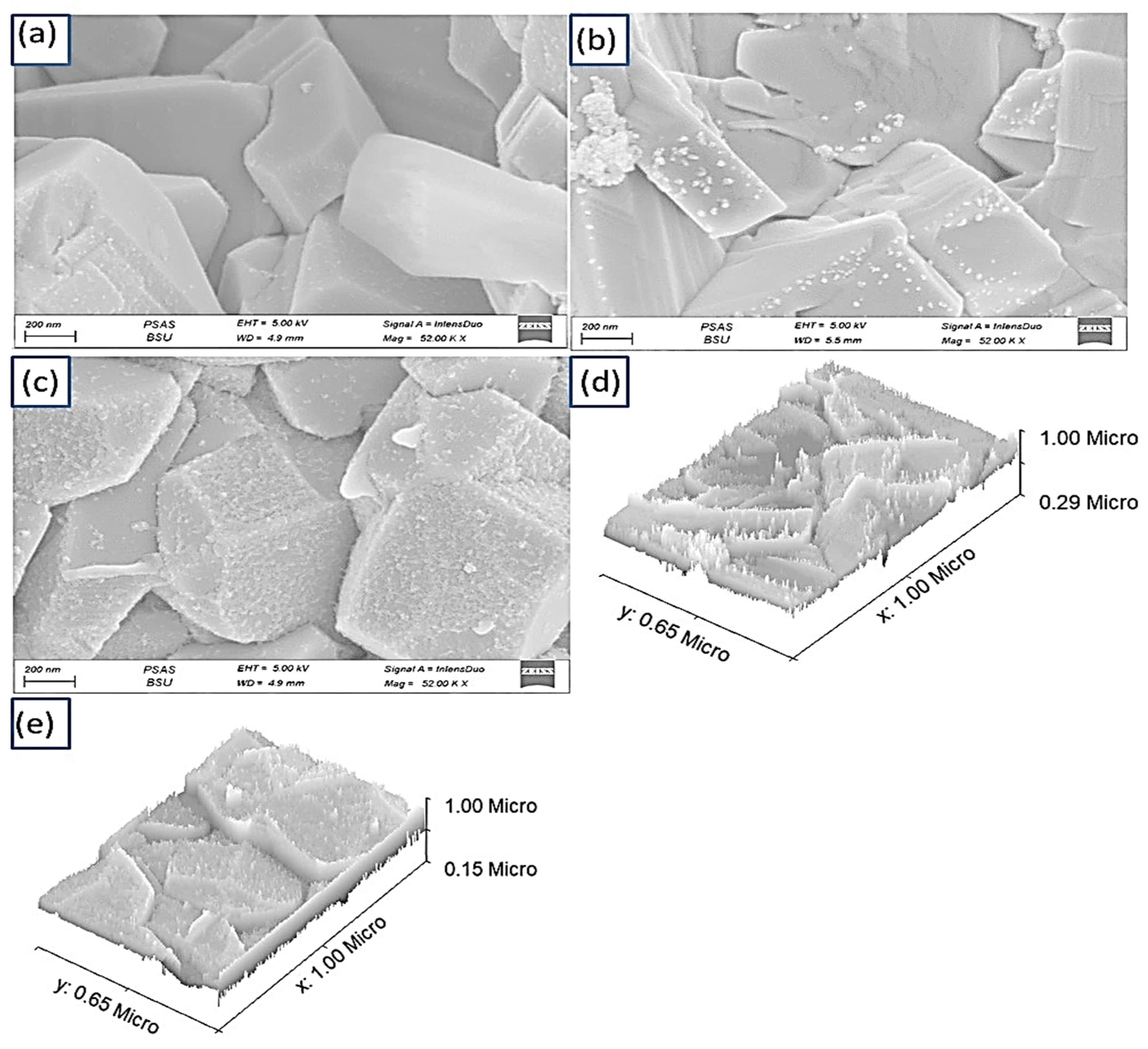
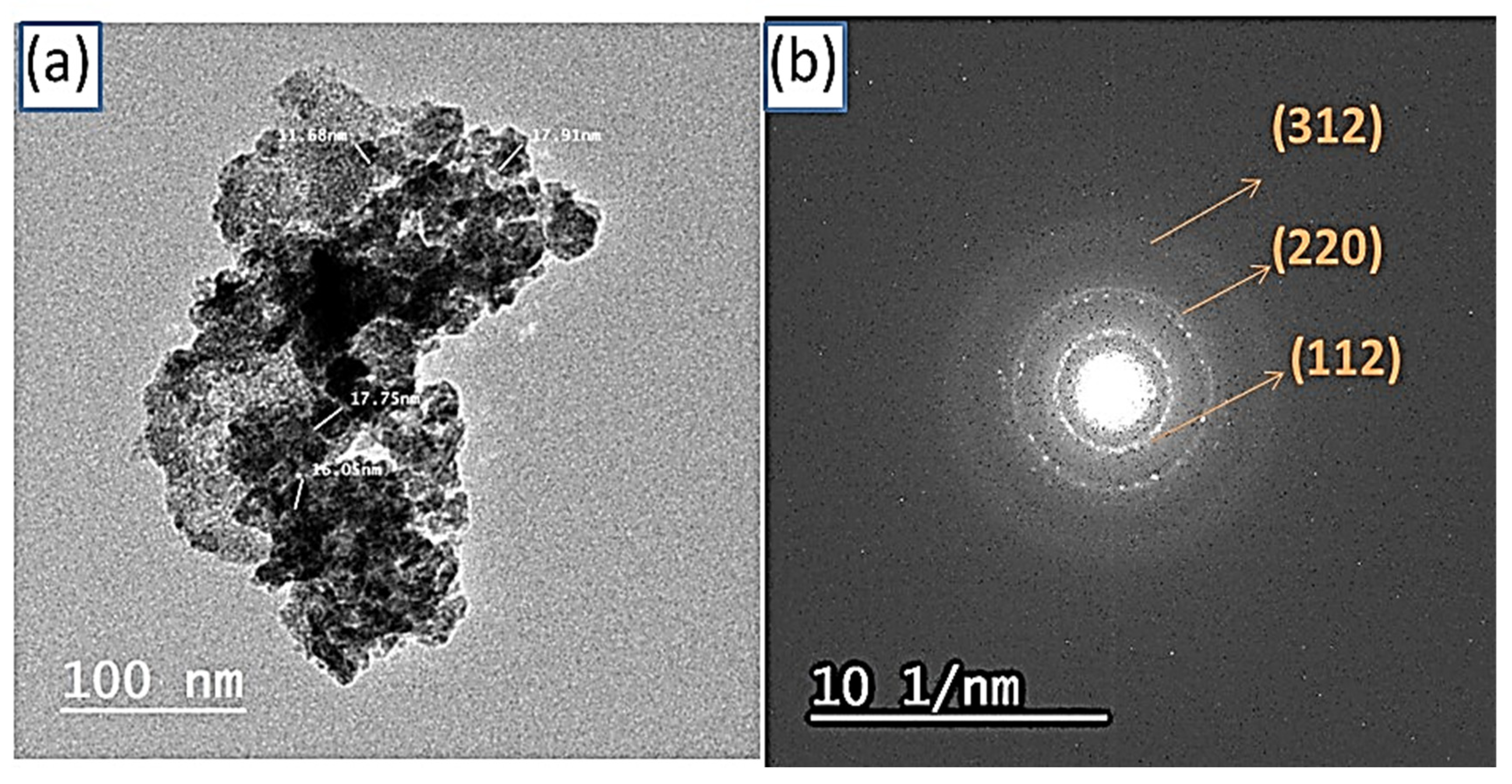
3.1. SEM and TEM Analyses
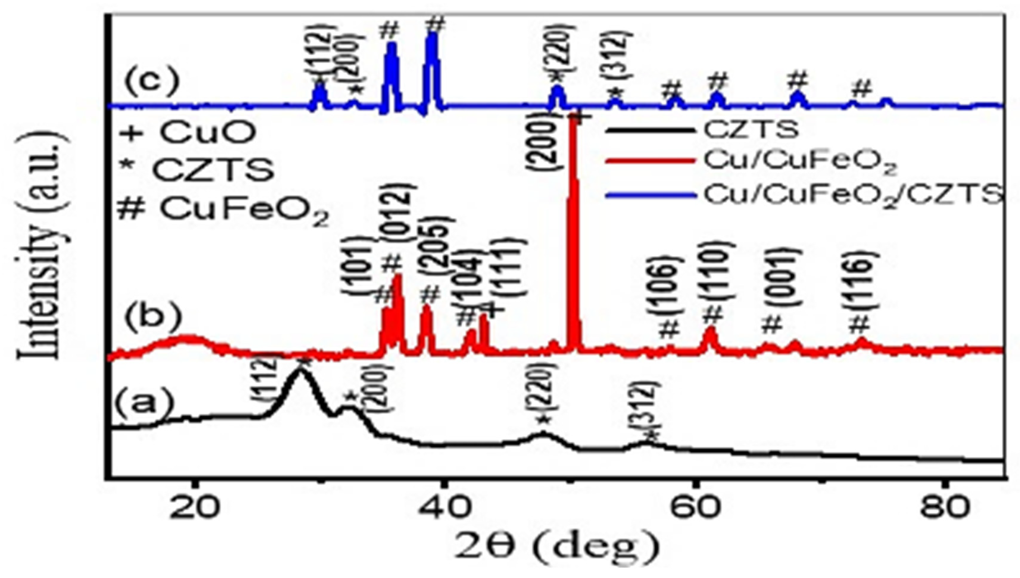
The surface morphology of Cu/CuFeO2/CZTS before and after addition of CZTS is investigated through the scanning electron microscopy (SEM). The SEM of CZTS is shown in Figure 1a. From the figure, it is clear that the crystalline grains are large, and no obvious flocs are formed on the surface, implying that the kestirite Cu2ZnSnS4 thin layer is essentially formed and that the crystallinity had significantly improved. The absence of pores confirms the compact particle of CZTS, although the high roughness of the surface is also observed. Some of the particles have a geometric shape, but they are nonuniform.
Figure 1b showed the SEM of Cu/CuFeO2 thin film, where the crystalline delafossite CuFeO2 thin film is presented, showing dense uniform grains without any cracks in its surface that help in enhancement of the optical features [20]. The highly crystalline nature of the formed particles predicts the highly crystalline XRD properties.
The SEM image of Cu/CuFeO2/CZTS thin film is shown in Figure 1c. It is shown that the particles grow, obviously displaying a uniform morphology with a particle size of approximately 350 nm, indicating that the Cu/CuFeO2/CZTS crystallinity is greatly improved. Moreover, the Cu/CuFeO2/CZTS film morphology displays a smooth surface and a homogeneous distribution of grains on the substrate without any cracks and holes at the surface film, confirming the stability of both Cu/CuFeO2 and CZTS layers. Moreover, the geometric shapes are enhanced in comparison to the previous CZTS shapes, in which the surface particles have a uniform shape. Additionally, there are additional very small particles that formed over the highly crystalline surface. These particles accept the film additional coating for covering and pores. These particles play a great role at the surface active site. From the above SEM results, the highly crystalline and free-of-cracks surface is a great feature for the electron generation and the photocatalytic properties [20,21,22,23,24,25,26,27,28].
The TEM of Cu/CuFeO2/CZTS thin layer is illustrated in Figure 2a, where the nanostructure size, which ranges from 11.68 nm to 17.9 nm of Cu/CuFeO2/CZTS, is appeared, while there are dark and grey color particles with overall particle size > 200nm that matches that seen in SEM image Figure 1c. The selected-area electron diffraction (SAED) is shown in Figure 2b, where the polycrystalline nature of Cu/CuFeO2/CZTS nanostructure is revealed, which is confirmed by the presence of large diffraction spots of the (312), (220), and (112) planes [29].
In addition to that, Figure 1d,e represents the cross section of CuFeO2 and CuFeO2/CZTS, respectively calculated using the theoretical program Gwydion. Under the deposition of CZTS, the cross section is increased by 0.14 µm. In addition to that, the roughness of the surface appears well, in which, after ZCTS deposition, the surface roughness decreases.

3.2. XRD Analyses

The XRD patterns of the three prepared thin films of CZTS, Cu/CuFeO2, and Cu/CuFeO2/CZTS are investigated. The XRD pattern of pure tetragonal CZTS phase is shown in Figure 3a, and it can be very closely matched with the typical pattern of kesterite CZTS. It displays four essential peaks at 56.08°, 47.84°, 32.2°, and 28.29°, corresponding to the (312), (220), (200), and (112) lattice planes, respectively. The outcomes are in line with the kesterite CZTS findings that have previously been presented [30,31]. Figure 3b showed the Cu/CuFeO2 XRD pattern. The crystal’s size is thought to be 24 nm. Based on the different peaks (Figure 3b), the CuFeO2 peaks are classified as two structural phases of CuFeO2: hexagonal 2H-CuFeO2 and rhombohedral 3R-CuFeO2 (JCPDS card numbers of 01-079-1546 and 00-039-0246, respectively). The 3R-CuFeO2 phase is considered as the major XRD pattern despite the presence of the 2H-CuFeO2 phase [32,33]. Moreover, in Figure 3b, the major CuFeO2 characteristic peaks are shown at 74.96°, 67.7°, 61.78°, 58.9°, 42°, 39°, 36°, and 35°, corresponding to the (116), (001) (110), (106), (104), (205), (012), and (101) lattice planes, respectively. the presence of CuO materials is confirmed through the peaks at 50°, 44°, for the growth direction of (200), (111), respectively. Figure 3c displays the XRD pattern of the Cu/CuFeO2/CZTS thin film. It is estimated that the crystal is 1.73 nm in size. The plot shows peaks at 74.96°, 67.7°, 61.78°, 56.08°, 47.84°, 39°, 36°, 32.2°, and 28.29°, corresponding to (116), (110), (012), (312), (220), (205), (012), (200), and (112). These peaks are almost exactly at the same points on the kesterite CZTS structure, which makes it evident that the sample belongs to the (312), (220), (200), and (112) planes of the kesterite CZTS. The CuFeO2 planes at lattice planes (116), (001) (110), (106), (104), (205), (012), and (101) are attributed to the other peaks (composite curve).

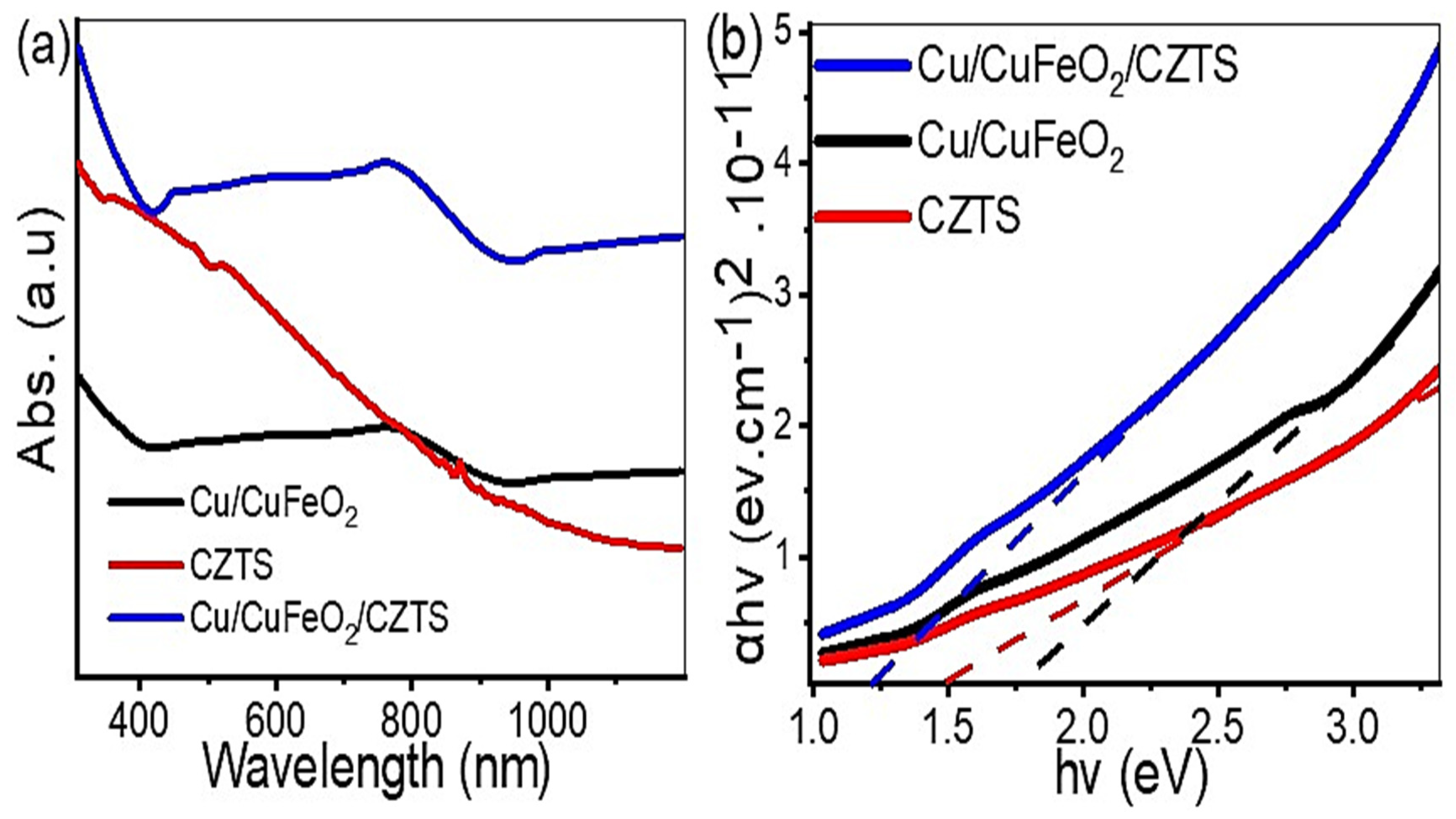
3.3. Optical Analyses of the Prepared Materials

To use the synthesized Cu/CuFeO2/CZTS sample as a photocatalytic H2 generator, it is required to examine its optical characteristics. The absorption curves of CZTS, Cu/CuFeO2, and Cu/CuFeO2/CZTS are illustrated in Figure 4a. It is demonstrated that the three films can absorb between 400 and 800 nm in the UV-vis and near IR ranges. It is also evident that adding CZTS to a Cu/CuFeO2 sample improves the intensity of Cu/CuFeO2 absorption. This can be explained by the fact that the bandgap of Cu/CuFeO2/CZTS is smaller than that of Cu/CuFeO2 thin films [31].
From Tauc’s equation [32], using the direct permitted transitions as a basis, we may estimate the optical band gap (Eg):
α hv   =   β ( hv     Eg ) 1 / 2
where β is a constant, h is the Planck constant, α is the absorption coefficient, and v is the light frequency. The absorbance, A, and absorption coefficient, α, are related to each other through the following equation, where d refers to thickness, [33]:
α   = 2.303   A / d
It is possible to determine the band gap value by extrapolating the (αhv)2 linear component vs. hv to intersect with the hv axis, as shown in Figure 4b. It is shown that the band gaps of CZTS, Cu/CuFeO2, and Cu/CuFeO2/CZTS are calculated as 1.49, 1.75, and 1.23 eV, respectively. From the Eg results, it can be implied that the optical absorbance of the Cu/CuFeO2/CZTS thin film can be improved after addition of CZTS. In conclusion, the Cu/CuFeO2/CZTS thin film can work as a highly efficient photodetector.

3.4. Testing Cu/CuFeO2/CZTS as a Photodetector

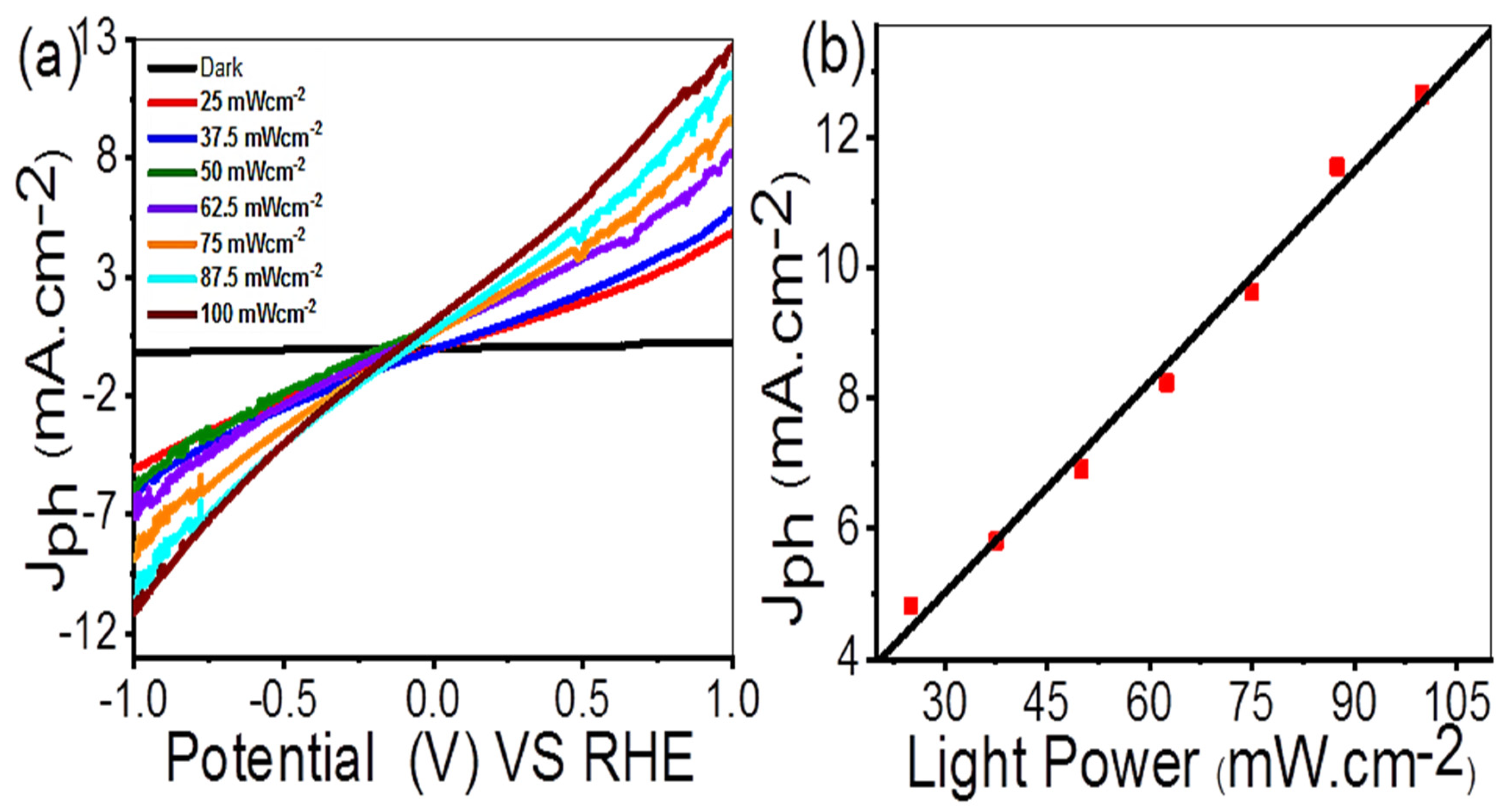
3.4.1. Effect of Light Power Intensity

Figure 5a shows the dark current (Jd) for Cu/CuFeO2/CZTS, where its value has changed from −0.23 to 0.2 mA·cm−2 under an applied potential from −1 to +1 V. This indicates the very small charge electrons of Cu/CuFeO2/CZTS that respond to the applied potential. In addition, under the dark condition, the free electrons are captured from the conduction band, and the oxygen molecules are adsorbed, as following [34,35]:
1 2 O 2 + 2 e 2 O 2
As a result, the resistivity increases, and the current density decreases. While at the light illumination, the electrons that will transfer from the valence band to the conduction band will generate electron–hole pairs. The holes rise to the surface, where they desorb oxygen ions, as follows:
hv e +   h +
2 h + +   O 2 O
As a result, the remaining electrons improve the conductivity of Cu/CuFeO2/CZTS, resulting in an increase in photocurrent. The adsorbed oxygen molecules on the Cu/CuFeO2/CZTS surface promote the release of electrons when the light source is turned off (dark). So, the sensor returns to its default state.
Figure 5b shows the produced photocurrent density at 1.0 V against the light power intensity for Cu/CuFeO2/CZTS. It is shown that the Jph results increase from 4.82 to 12.64 mA·cm−2, with increasing power intensity from 25 to 100 mW/cm2. The nonlinearity between photocurrent density and light intensity indicates the transportation reaction of the complex electron–hole [36]. This demonstrates that increasing the light power intensity results in the creation of additional carriers on the material surface as a result of increasing electron excitation from VB to CB [36].
A simple power-law can be used to describe the relationship between light intensity and photocurrent, as follows:
J ph = BP y
where P is the incident light power, B represents a wavelength constant, and y shows the exponent parameter that determines the response rate through calculation of photodetector’s (photocurrent) sensitivity to incident light intensity. Moreover, the exponent parameter y refers to the electron–hole recombination, generation, and carriers trapping in photodetectors through complex processes [37]. Using the previous equation to fit the experimental results, the red line in Figure 5b shows that y is practically integer exponent (0.99), which implies a good photosensing ability [37]. These results suggest that Cu/CuFeO2/CZTS can work as an excellent photodetector for the light power intensity.
Peng specifies the linear dynamic range (LDR, usually quoted in dB), as follows [38]:
LDR = 20 log J ph J d
The relatively large LDR value is calculated to be 193.58 dB, at 100 mW/cm2, indicating the linear responsiveness of the device.

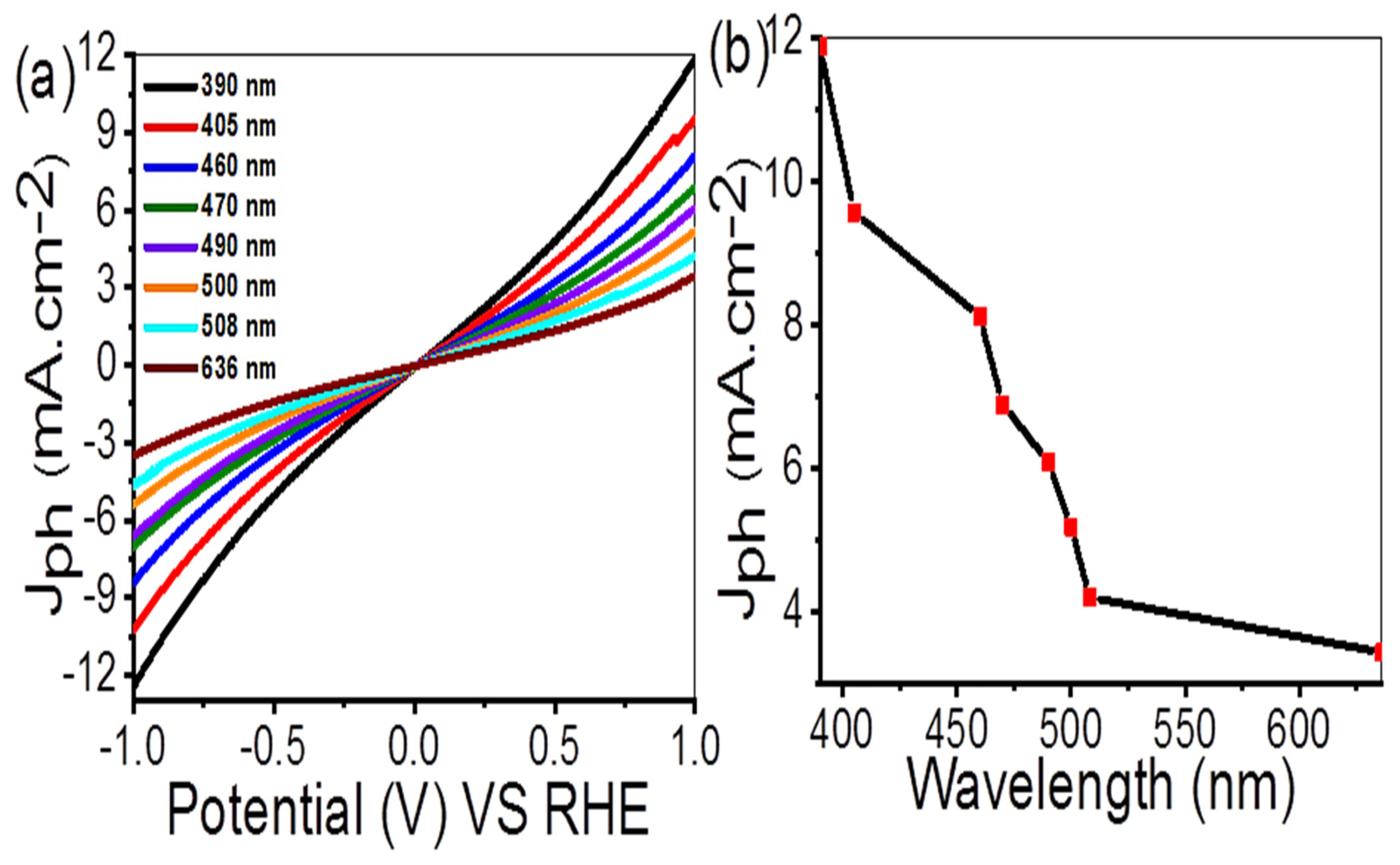
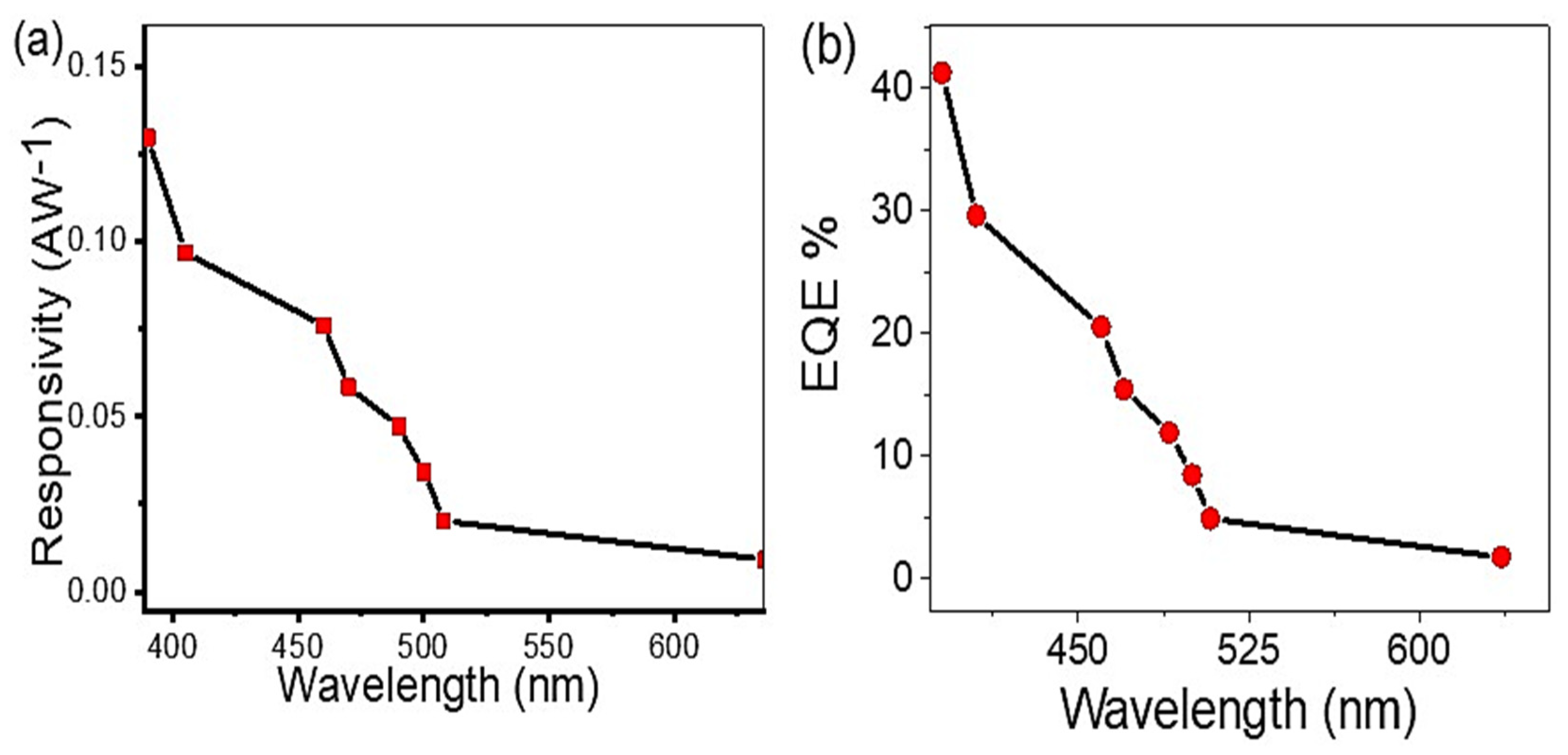
3.4.2. Light Wavelength

To obtain the spectral response of the Cu/CuFeO2/CZTS device, the photocurrent-voltage characteristics (Jph–V) are recorded using different monochromatic wavelengths. Figure 6a represents the Jph–V relation under monochromatic wavelengths from UV to NIR (390 to 636 nm). It is shown that the Jph value decreases as the wavelength increases, from 390 to 636 nm. Figure 6b shows the Jph results at +1 V with different monochromatic light under illumination. It is shown that, by increasing the optical wavelengths from 390 to 636 nm, the Jph values decreased. The minimum Jph results are recoded at a wavelength of 636 nm.
The performance of the photodetector is investigated from the determination of some parameters, such as the specific detectivity (D), the photoresponsivity (R), and the external quantum efficiency (EQE) [39]. The relationship between the photocurrent density and the light intensity can be used to determine the R-value, in which Jph and Jd represent the current density in light and dark, respectively [40]. This can be determined from the I–V characteristics at +1 V, as follows [41]:
R = J ph   J d light   power
Equation (9) can be used to calculate the specific detectivity of the photodetector, as follows, where e indicates the electron charge and A represents the surface area [40]:
D = R   A   / 2   e   J d  
Figure 7a shows the responsivity of the photodetector with the applied wavelengths at 100 mW. The maximum photoresponse is R = 127 mAW−1 at about 390 nm. This agrees well with the Jph results, Figure 6. Additionally, the maximum specific detectivity is D = 1.7 × 10¹⁰ Jones at about 390 nm.
The relationship between incident light photon flux and generated electrons is known as the external quantum efficiency (EQE) [42]. The photon flow is related to the light intensity. The EQE value can be estimated from the R-value, depending on the wavelength (λ), as follows [43]:
EQE =   R   1240 λ 100 %
By increasing the light intensity from 25 to 100 mWcm−2, the EQE for Cu/CuFeO2/CZTS is decreased from 41.5% to 2.04%, respectively, as mentioned in Figure 7b.
From all the above results, we can deduce that the investigated Cu/CuFeO2/CZTS photodetector performs better in terms of quantum efficiency and photoresponsivity. As a result, the fabricated Cu/CuFeO2/CZTS functions well as a unique photodetector for efficiently detecting the light power intensity and the wavelengths.

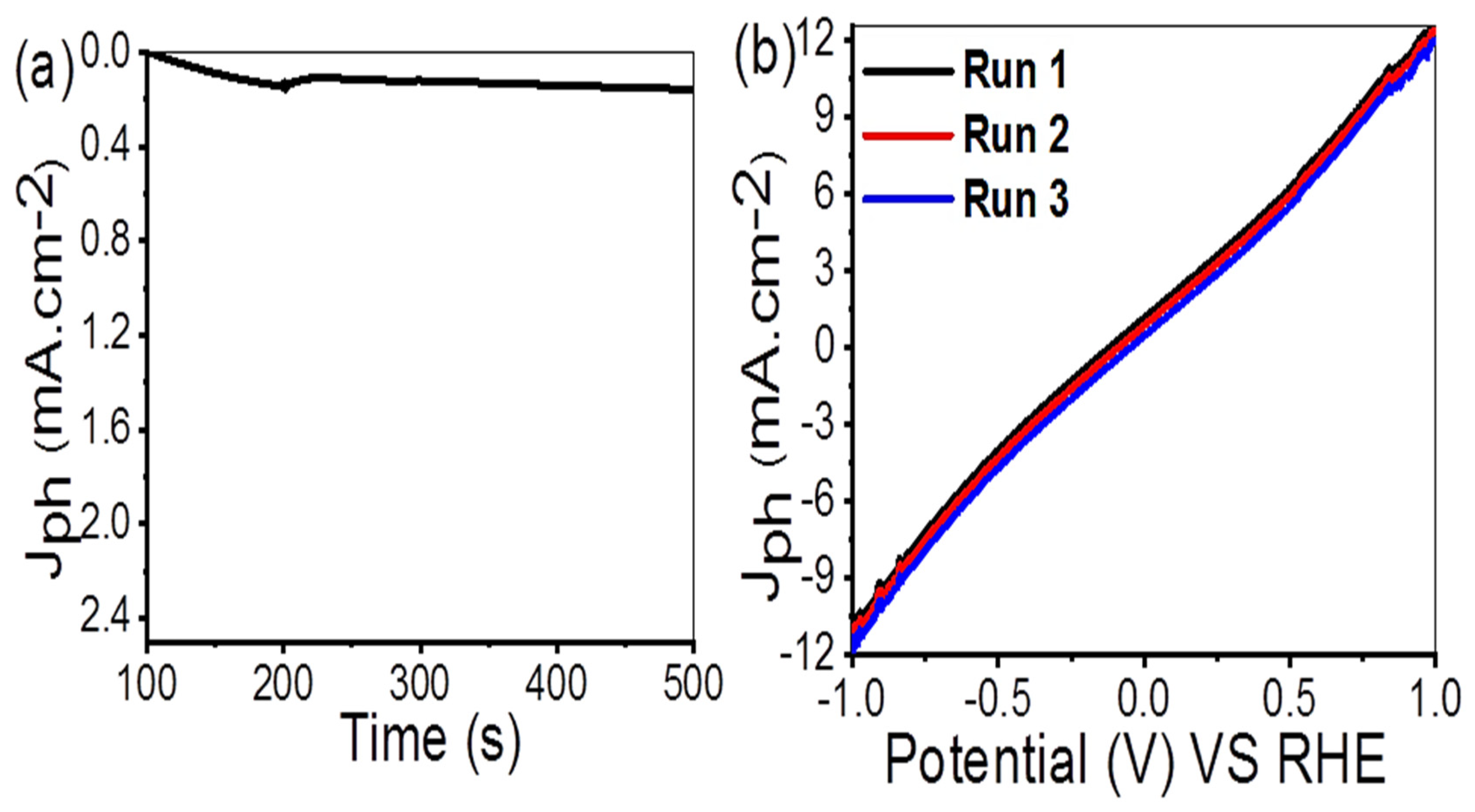
3.4.3. Reproducibility and Stability
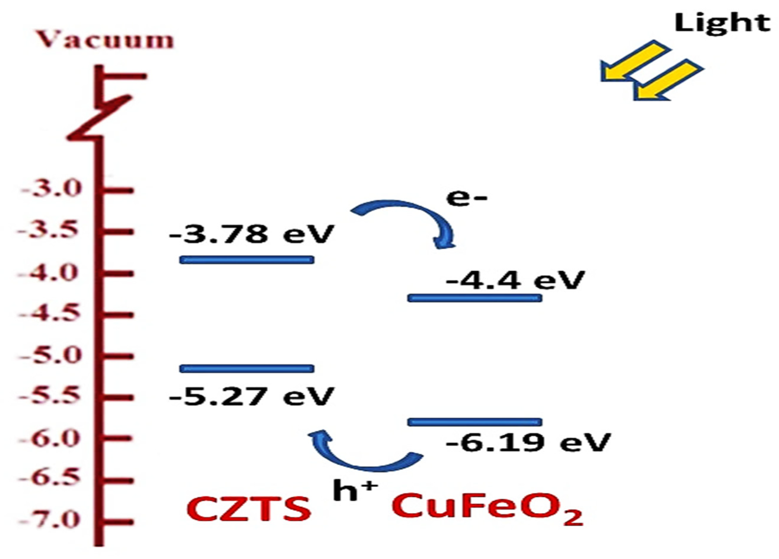
Figure 8 shows the reproducibility and the stability of the fabricated Cu/CuFeO2/CZTS photodetector. The stability of the photoelectrode is carried out by applying 1.0 V to the photodetector and measuring the produced Jph. From Figure 8a, the first 250 s showed a decrease in the Jph values, then the Jph values were almost constant until 500 s, indicating the acceptable stability of the prepared Cu/CuFeO2/CZTS. The adsorption of O2 molecules on the Cu/CuFeO2/CZTS surface causes a very small photocurrent change over time. This high stability of the prepared Cu/CuFeO2/CZTS photodetector is related to its construction, which is based on the inorganic stable materials [32].
The prepared Cu/CuFeO2/CZTS photoelectrode is tested multiple times under light intensities of 25 and 100 mW/cm2 to determine reproducibility. From Figure 8b, all of the runs had very identical values. This confirms a good reproducibility and stability of the prepared Cu/CuFeO2/CZTS photodetector.

3.5. Mechanism

Energy band theory is the basis for the Cu/CuFeO2/CZTS photodetector’s operation. According to previous research, the energy bandgap of CZTS is approximately 1.46–1.6 eV [44,45]. Under illumination, the CZTS produces electron–hole pairs, which participate in the production of photocurrent in the photodetector. Meanwhile, the surface plasmon-induced electron collective oscillation in CuFeO2 can also result in an increase in the electromagnetic fields [46]. Additionally, the photocurrent of the photodetector device was improved by the CZTS’s strong light absorption and the activation of hot electrons.
The carriers’ (holes and electrons) diffusion for the CuFeO2/CZTS connection proceeds until the Fermi energy (EF) is equal in both materials. As a result, there is band bending at the CuFeO2/CZTS contact, and a depletion area is created (or built-in electric field). The resultant electron–hole pairs can be effectively separated by the internal electric field. Due to surface plasmon resonance, heated electrons and holes are produced at the Fermi level of the CuFeO2 layer when it is exposed to light. In addition, CuFeO2 has a work function that is approximately lower than CZTS. CuFeO2 cannot inject holes into CZTS because the energy gap between the Fermi level and CZTS valence band is too high. The general mechanism for the electron transfer under the light illumination is mentioned in Figure 9.
However, because the height of the barrier between the CZTS conduction band and the CuFeO2 Fermi level is low, hot electrons can go from CuFeO2 to the CZTS conduction band after passing the barrier [44,45]. By doing this, the carrier’s recombination is stopped, allowing for continuous electron flow into the device and the creation of photocurrent. Finally, Table 1 compares the performance of the constructed Cu/CuFeO2/CZTS photodetector with earlier research.

4. Conclusions

A novel Cu/CuFeO2/CZTS photodetector is prepared with high efficiency, low cost, and high stability for industrial applications. The photodetector is investigated at several light intensities (25 to 100 mW/cm2) and wavelengths (390 to 636 nm). The morphological, chemical, and optical properties are discussed using several analyses, such as SEM, TEM, XRD, and UV–Vis. From SEM and TEM results of Cu/CuFeO2/CZTS thin film, the morphology has a homogeneous nature with particles size around 350 nm, demonstrating a significant improvement in morphology. From XRD analysis of Cu/CuFeO2/CZTS, the high intensity of the generated peaks indexed to hexagonal (2H) CuFeO2 and kesterite CZTS crystal structures, revealing a compact highly crystal material. The crystal sizes of Cu/CuFeO2 and Cu/CuFeO2/CZTS thin films are estimated to be 24 nm and 1.73 nm, respectively, implying that the Cu/CuFeO2/CZTS crystalline quality is being improved. From optical analysis, CZTS, Cu/CuFeO2, and Cu/CuFeO2/CZTS thin films recoded band gaps of 1.49, 1.75, and 1.23 eV, respectively. According to the band gap measurements, the optical absorption of the Cu/CuFeO2/CZTS photodetector has clearly increased. From the electrochemical measurements, the Cu/CuFeO2/CZTS photodetector records efficient EQE, D, and R results of 41.5%, 1.7 × 10¹⁰ Jones, and 127mAW−1, respectively. We look forward to widening the applications of the fabricated Cu/CuFeO2/CZTS photodetector in the smart screens, light-sensing devices, and space industry.

Author Contributions

Conceptualization, A.H.A., A.S.H., A.M.A., M.S., A.A.A.-K., F.M.A., S.M.A., S.A.E.K. and M.R.; methodology, A.H.A., A.S.H., A.M.A., M.S., A.A.A.-K., F.M.A., S.M.A., S.A.E.K. and M.R.; software, A.H.A., A.S.H., A.M.A., M.S., A.A.A.-K., F.M.A., S.M.A., S.A.E.K. and M.R.; validation, A.H.A., A.S.H., A.M.A., M.S., A.A.A.-K., F.M.A., S.M.A., S.A.E.K. and M.R.; formal analysis, A.H.A., A.S.H., A.M.A., M.S., A.A.A.-K., F.M.A., S.M.A., S.A.E.K. and M.R.; resources, A.H.A., A.S.H., A.M.A., M.S., A.A.A.-K., F.M.A., S.M.A., S.A.E.K. and M.R.; data curation, A.H.A., A.S.H., A.M.A., M.S., A.A.A.-K., F.M.A., S.M.A., S.A.E.K. and M.R.; writing—original draft preparation, A.H.A., A.S.H., A.M.A., M.S., A.A.A.-K., F.M.A., S.M.A., S.A.E.K. and M.R.; writing—review and editing, A.H.A., A.S.H., A.M.A., M.S., A.A.A.-K., F.M.A., S.M.A., S.A.E.K. and M.R.; visualization, A.H.A., A.S.H., A.M.A., M.S., A.A.A.-K., F.M.A., S.M.A., S.A.E.K. and M.R.; supervision, A.M.A., M.S., A.A.A.-K., F.M.A. and M.R.; project administration, F.M.A.; funding acquisition, F.M.A. All authors have read and agreed to the published version of the manuscript.

Funding

The authors extend their appreciation to the Deanship of Scientific Research at Princess Nourah bint Abdulrahman University for funding this work through the Princess Nourah bint Abdulrahman University Researchers Supporting Project (number PNURSP2022R42), Princess Nourah bint Abdulrahman University, Riyadh, Saudi Arabia.

Institutional Review Board Statement

Not applicable.

Informed Consent Statement

Not applicable.

Data Availability Statement

Not applicable.

Acknowledgments

The authors extend their appreciation to the Deanship of Scientific Research at Princess Nourah bint Abdulrahman University for funding this work through the Princess Nourah bint Abdulrahman University Researchers Supporting Project (number PNURSP2022R42), Princess Nourah bint Abdulrahman University, Riyadh, Saudi Arabia.

Conflicts of Interest

The authors declare no conflict of interest.

References

  1. Yin, W.; Yang, J.; Zhao, K.; Cui, A.; Zhou, J.; Tian, W.; Chu, J. High responsivity and external quantum efficiency photodetectors based on solution-processed Ni-doped CuO films. ACS Appl. Mater. Interfaces 2020, 12, 11797–11805. [Google Scholar] [CrossRef]
  2. Gao, Y.; Xu, J.; Shi, S.; Dong, H.; Cheng, Y.; Wei, C.; Li, L. TiO2 nanorod arrays based self-powered UV photodetector: Heterojunction with NiO nanoflakes and enhanced UV photoresponse. ACS Appl. Mater. Interfaces 2018, 10, 11269–11279. [Google Scholar] [CrossRef]
  3. Shashanka, R.; Esgin, H.; Yilmaz, V.; Caglar, Y. Fabrication and characterization of green synthesized ZnO nanoparticle based dye-sensitized solar cells. Adv. Mater. Devices 2020, 5, 185–191. [Google Scholar] [CrossRef]
  4. Bera, A.; Deb, K.; Chattopadhyay, K.; Thapa, R.; Saha, B. Mixed phase delafossite structured p type CuFeO2/CuO thin film on FTO coated glass and its Schottky diode characteristics. Microelectron. Eng. 2016, 162, 23–26. [Google Scholar] [CrossRef]
  5. Zhang, N.; Liu, X.; Lim, D.; Gong, H. A New Highly Conductive Direct Gap p-Type Semiconductor La1–x Y x CuOS for Dual Applications: Transparent Electronics and Thermoelectricity. ACS Appl. Mater. Interfaces 2020, 12, 6090–6096. [Google Scholar] [CrossRef]
  6. Min, W.; Park, K.; Kim, H.; Lee, J.; Park, K.; Kim, D.; Kim, H. Switching enhancement via a back-channel phase-controlling layer for p-type copper oxide thin-film transistors. ACS Appl. Mater. Interfaces 2020, 12, 24929–24939. [Google Scholar] [CrossRef]
  7. Gao, F.; Liu, X.; Zhang, J.; Song, M.; Li, N. Photovoltaic properties of the p-CuO/n-Si heterojunction prepared through reactive magnetron sputtering. J. Appl. Phys. 2012, 111, 084507. [Google Scholar] [CrossRef]
  8. Prabhu, R.; Saritha, A.; Shijeesh, M.; Jayaraj, M. Fabrication of p-CuO/n-ZnO heterojunction diode via sol-gel spin coating technique. Mater. Sci. Eng. 2017, 220, 82–90. [Google Scholar] [CrossRef]
  9. Hong, Q.; Cao, Y.; Xu, J.; Lu, H.; He, J.; Sun, J. Self-powered ultrafast broadband photodetector based on p–n heterojunctions of CuO/Si nanowire array. ACS Appl. Mater. Interfaces 2014, 6, 20887–20894. [Google Scholar] [CrossRef]
  10. Bera, A.; Deb, K.; Bera, T.; Sinthika, S.; Thapa, R.; Saha, B. Effect of Mg substitution in delafossite structured CuFeO2 thin film deposited on FTO coated glass substrate and its diode characteristics. Thin Solid Film. 2017, 642, 316–323. [Google Scholar] [CrossRef]
  11. Kawazoe, H.; Yasukawa, M.; Hyodo, H.; Kurita, M.; Yanagi, H.; Hosono, H. P-type electrical conduction in transparent thin films of CuAlO2. Nature 1997, 389, 939–942. [Google Scholar] [CrossRef]
  12. Zhang, B.; Thampy, S.; Dunlap-Shohl, W.; Xu, A.; Zheng, W.; Cao, Y.; Hsu, J. Mg doped CuCrO2 as efficient hole transport layers for organic and perovskite solar cells. Nanomaterials 2019, 9, 1311. [Google Scholar] [CrossRef] [Green Version]
  13. Hermans, Y.; Klein, A.; Sarker, H.P.; Huda, M.N.; Junge, H.; Toupance, T.; Jaegermann, W. Pinning of the Fermi Level in CuFeO2 by Polaron Formation Limiting the Photovoltage for Photochemical Water Splitting. Adv. Funct. Mater. 2020, 30, 1910432. [Google Scholar] [CrossRef] [Green Version]
  14. Vojkovic, S.; Fernandez, J.; Elgueta, S.; Vega, F.E.; Rojas, S.D.; Wheatley, R.A.; Seifert, B.; Wallentowitz, S.; Cabrera, A.L. Band Gap Determination in Multi-Band-Gap CuFeO2 Delafossite Epitaxial Thin Film by Photoconductivity. SN Appl. Sci. 2019, 1, 1322. [Google Scholar] [CrossRef] [Green Version]
  15. Alkallas, F.H.; Ben Gouider Trabelsi, A.; Alrebdi, T.A.; Ahmed, A.M.; Rabia, M. Development of a Highly Efficient Optoelectronic Device Based on CuFeO2/CuO/Cu Composite Nanomaterials. Materials 2022, 15, 6857. [Google Scholar] [CrossRef]
  16. Lee, S.; Lee, W.; Jang, Y.; Kim, B.; Bae, T.; Cho, J.; Jang, J. Sol-gel processed p-type CuO phototransistor for a near-infrared sensor. IEEE Electron. Device Lett. 2017, 39, 47–50. [Google Scholar] [CrossRef]
  17. Ruzgar, S.; Pehlivanoglu, S. The effect of Fe dopant on structural, optical properties of TiO2 thin films and electrical performance of TiO2 based photodiode. Superlattices Microstruct. 2020, 145, 106636. [Google Scholar] [CrossRef]
  18. Ruzgar, S.; Caglar, Y.; Polat, O.; Sobola, D.; Caglar, M. The influence of Fe substitution into photovoltaic performance of p-CuO/n-Si heterojunctions. J. Mater. Sci. Mater. Electron. 2021, 32, 20755–20766. [Google Scholar] [CrossRef]
  19. Li, J.; Wu, Q.; Wu, J. Synthesis of Nanoparticles via Solvothermal and Hydrothermal Methods. Nanoparticles 2016, 12, 295–328. [Google Scholar]
  20. Wang, L.; Wang, W.; Sun, S. A simple template-free synthesis of ultrathin Cu2ZnSnS4 nanosheets for highly stable photocatalytic H2 evolution. J. Mater. Chem. 2012, 22, 6553–6555. [Google Scholar] [CrossRef]
  21. Li, X.; Wang, S.; Liao, H.; Yang, S.; Wang, T.; Liu, X. The preparation of Cu2ZnSnS4 thin film solar cell based on oxygen containing precursor. J. Mater. Sci. Mater. Electron. 2020, 31, 19309–19317. [Google Scholar] [CrossRef]
  22. Li, Q.; Yu, H.; Cui, Y.; Wang, J.; Du, J.; Wang, M.; Gao, S. Effect of Sulfurization Temperature on the Preparation of Cu2ZnSnS4 Thin Films for Solar Cells via a Nanoink Coating Method. Int. J. Electrochem. Sci. 2021, 16, 210558. [Google Scholar] [CrossRef]
  23. Yanalak, G.; Sarılmaz, A.; Aslan, E.; Ozel, F.; Patir, I. Photocatalytic hydrogen evolution reaction activity comparable to 1-D nanofiber materials exhibited by the kesterite nanorods catalysts. Renew. Energy 2020, 150, 469–475. [Google Scholar] [CrossRef]
  24. Ha, E.; Lee, L.; Man, H.; Tsang, S.; Wong, K. Morphology-controlled synthesis of Au/Cu2FeSnS4 core–shell nanostructures for plasmon-enhanced photocatalytic hydrogen generation. ACS Appl. Mater. Interfaces 2015, 7, 9072–9077. [Google Scholar] [CrossRef] [PubMed]
  25. Yu, X.; Shavel, A.; An, X.; Luo, Z.; Ibanez, M.; Cabot, A. Cu2ZnSnS4-Pt and Cu2ZnSnS4-Au heterostructured nanoparticles for photocatalytic water splitting and pollutant degradation. J. Am. Chem. Soc. 2014, 136, 9236–9239. [Google Scholar] [CrossRef]
  26. Guo, Q.; Hillhouse, H.; Agrawal, R. Synthesis of Cu2ZnSnS4 nanocrystal ink and its use for solar cells. J. Am. Chem. Soc. 2009, 131, 11672–11673. [Google Scholar] [CrossRef] [PubMed]
  27. Steinhagen, C.; Panthani, M.; Akhavan, V.; Goodfellow, B.; Koo, B.; Korgel, B. Synthesis of Cu2ZnSnS4 nanocrystals for use in low-cost photovoltaics. J. Am. Chem. Soc. 2009, 131, 12554–12555. [Google Scholar] [CrossRef]
  28. Singh, A.; Geaney, H.; Laffir, F.; Ryan, K. Colloidal synthesis of wurtzite Cu2ZnSnS4 nanorods and their perpendicular assembly. J. Am. Chem. Soc. 2012, 134, 2910–2913. [Google Scholar] [CrossRef] [Green Version]
  29. Zhou, Y.; Zhou, W.; Du, Y.; Li, M.; Wu, S. Sphere-like kesterite Cu2ZnSnS4 nanoparticles synthesized by a facile solvothermal method. Mater. Lett. 2011, 65, 1535–1537. [Google Scholar] [CrossRef]
  30. Nishi, H.; Kuwabata, S.; Torimoto, T. Composition-dependent photoelectrochemical properties of nonstoichiometric Cu2ZnSnS4 nanoparticles. J. Phys. Chem. 2013, 117, 21055–21063. [Google Scholar] [CrossRef]
  31. Ju, D.; Jiang, X.; Xiao, H.; Chen, X.; Hu, X.; Tao, X. Narrow band gap and high mobility of lead-free perovskite single crystal Sn-doped MA3Sb2I9. J. Mater. Chem. 2018, 6, 20753–20759. [Google Scholar] [CrossRef]
  32. Fadel, M.; Rabia, M.; Ezzat, S.; Mansour, N.; Saeed, E.; Sayyah, S. Effect of annealing temperature on VO2(M)/ITO film nanomaterials for thermochromic smart windows application and study its contact angle. J. Nanophotonics 2018, 12, 016009. [Google Scholar]
  33. Chen, C.; Yu, W.; Liu, T.; Cao, S.; Tsang, Y. Graphene oxide/WS2/Mg-doped ZnO nanocomposites for solar-light catalytic and anti-bacterial applications. Sol. Energy Mater. Sol. Cells 2017, 160, 43–53. [Google Scholar] [CrossRef]
  34. Shinde, N.M.; Deshmukh, P.R.; Patil, S.V.; Lokhande, C.D. Development of polyaniline/Cu2ZnSnS4 (CZTS) thin film based heterostructure as room temperature LPG sensor. Sens. Actuators A Phys. 2013, 193, 79–86. [Google Scholar] [CrossRef]
  35. Yu, X.; Zhang, X.; Wang, H.; Feng, G. High coverage water adsorption on the CuO(111) surface. Appl. Surf. Sci. 2017, 425, 803–810. [Google Scholar] [CrossRef]
  36. Wang, X.; Tian, W.; Liao, M.; Bando, Y.; Golberg, D. Recent advances in solution-processed inorganic nanofilm photodetectors. Chem. Soc. Rev. 2014, 43, 1400–1422. [Google Scholar] [CrossRef] [PubMed]
  37. Luo, L.; Zeng, B.; Xie, L.; Yu, C.; Liang, Q.; Wu, F.; Hu, J. Light trapping and surface plasmon enhanced high-performance NIR photodetector. Sci. Rep. 2014, 4, 3914. [Google Scholar] [CrossRef] [Green Version]
  38. Wang, W.; Zhang, P.; Yu, J.; Wang, Y.; Zheng, D.; Zheng, W.; Pang, J. Constraints on mountain building in the northeastern Tibet: Detrital zircon records from synorogenic deposits in the Yumen Basin. Sci. Rep. 2016, 6, 27604. [Google Scholar] [CrossRef] [Green Version]
  39. Zhao, H.; Ouyang, B.; Han, L.; Mishra, Y.; Zhang, Z.; Yang, Y. Conjuncted photo-thermoelectric effect in ZnO–graphene nanocomposite foam for self-powered simultaneous temperature and light sensing. Sci. Rep. 2020, 10, 11864. [Google Scholar] [CrossRef]
  40. Jia, R.; Zhao, D.; Gao, N.; Liu, D. Polarization enhanced charge transfer: Dual-band GaN-based plasmonic photodetector. Sci. Rep. 2017, 7, 40483. [Google Scholar] [CrossRef] [Green Version]
  41. Kunwar, S.; Pandit, S.; Jeong, J.; Lee, J. Improved photoresponse of UV photodetectors by the incorporation of plasmonic nanoparticles on GaN through the resonant coupling of localized surface plasmon resonance. Nano-Micro Lett. 2020, 12, 91. [Google Scholar] [CrossRef] [PubMed] [Green Version]
  42. Bell, S.; Will, G.; Bell, J. Light intensity effects on photocatalytic water splitting with a titania catalyst. Int. J. Hydrog. Energy 2013, 38, 6938–6947. [Google Scholar] [CrossRef]
  43. Shaban, M.; Rabia, M.; El-Sayed, A.A.; Ahmed, A.; Sayed, S. Photocatalytic properties of PbS/graphene oxide/polyaniline electrode for hydrogen generation. Sci. Rep. 2017, 7, 14100. [Google Scholar] [CrossRef] [PubMed] [Green Version]
  44. Malerba, C.; Biccari, F.; Ricardo, C.; Valentini, M.; Chierchia, R.; Muller, M.; Mittiga, A. CZTS stoichiometry effects on the band gap energy. J. Alloy. Compd. 2014, 582, 528–534. [Google Scholar] [CrossRef]
  45. Khammar, M.; Ynineb, F.; Guitouni, S.; Bouznit, Y.; Attaf, N. Crystallite size and intrinsic strain contribution in band gap energy redshift of ultrasonic-sprayed kesterite CZTS nanostructured thin films. Appl. Phys. A 2020, 126, 398. [Google Scholar] [CrossRef]
  46. Aqaei, F.; Zare, M.; Shafiekhani, A. Role of plasmonic Au nanoparticles embedded in the diamond-like carbon overlayer in the performance of CuFeO2 solar photocathodes. J. Solid State Electrochem. 2021, 25, 1139–1150. [Google Scholar] [CrossRef]
  47. Madusanka, H.; Herath, H.; Fernando, C. High photoresponse performance of self-powered n-Cu2O/p-CuI heterojunction based UV-Visible photodetector. Sens. Actuators A Phys. 2019, 296, 61–69. [Google Scholar] [CrossRef]
  48. Guo, D.; Li, W.; Wang, D.; Meng, B.; Fang, D.; Wei, Z. High performance Cu2O film/ZnO nanowires self-powered photodetector by electrochemical deposition. Chin. Phys. B 2020, 29, 098504. [Google Scholar] [CrossRef]
  49. Wu, H.; Ma, C.; Zhang, J.; Cao, H.; Lin, R.; Bai, W.; Chu, J. High-Performance Photodetectors with an Ultrahigh Photoswitching Ratio and a Very Fast Response Speed in Self-Powered Cu2ZnSnS4/CdS PN Heterojunctions. ACS Appl. Electron. Mater. 2021, 3, 4135–4143. [Google Scholar] [CrossRef]
  50. Lai, B.; Shen, H.; Zhao, Q.; Li, Y.; Fan, W. Self-driven heterostructure photodetector of sputtered CZTS film on c-Si with an inverted pyramid structure. Ceram. Int. 2022, 48, 2105–2111. [Google Scholar] [CrossRef]
  51. Gour, K.; Singh, O.; Bhattacharyya, B.; Parmar, R.; Husale, S.; Senguttuvan, T.; Singh, V. Enhanced photoresponse of Cu2ZnSn(S,Se)4 based photodetector in visible range. J. Alloy. Compd. 2017, 694, 119–123. [Google Scholar] [CrossRef]
  52. Han, M.; Sun, J.; Peng, M.; Han, N.; Chen, Z.; Liu, D.; Yang, Z. Controllable growth of lead-free all-inorganic perovskite nanowire array with fast and stable near-infrared photodetection. J. Phys. Chem. C 2019, 123, 17566–17573. [Google Scholar] [CrossRef]
  53. Cao, F.; Tian, W.; Wang, M.; Wang, M.; Li, L. Stability enhancement of lead-free CsSnI3 perovskite photodetector with reductive ascorbic acid additive. InfoMat 2020, 2, 577–584. [Google Scholar] [CrossRef] [Green Version]
  54. Han, X.; Liang, J.; Yang, J.; Soni, K.; Fang, Q.; Wang, W.; Lou, J. Lead-free double perovskite Cs2SnX6: Facile solution synthesis and excellent stability. Small 2019, 15, 1901650. [Google Scholar] [CrossRef]
  55. Tao, S.; Chen, Y.; Cui, J.; Zhou, H.; Yu, N.; Gao, X.; Wu, M. Organic–inorganic hybrid (CH3NH3)2FeCuI4Cl2 and (CH3NH3)2InCuI6 for ultraviolet light photodetectors. Chem. Commun. 2020, 56, 1875–1878. [Google Scholar] [CrossRef]
  56. Chang, C.; Chen, W.; Chen, Y.; Ding, F.; Liu, Z. Recent progress on two-dimensional materials. Acta Phys. Chim. Sin. 2021, 37, 2108017. [Google Scholar] [CrossRef]
  57. Lan, T.; Fallatah, A.; Suiter, E.; Padalkar, S. Size controlled copper(I)oxide nanoparticles influence sensitivity of glucose biosensor. Sensors 2017, 17, 1944. [Google Scholar] [CrossRef] [Green Version]
  58. An, Q.; Meng, X.; Xiong, K.; Qiu, Y. Self-powered ZnS nanotubes/Ag nanowires MSM UV photodetector with high on/off ratio and fast response speed. Sci. Rep. 2017, 7, 4885. [Google Scholar] [CrossRef]
Figure 1. The SEM images of the prepared (a) CZTS, (b) Cu/CuFeO2, and (c) Cu/CuFeO2/CZTS thin films. Theoretical image cross section for (d) Cu/CuFeO2 and (e) Cu/CuFeO2/CZTS thin film.
Photonics 09 00979 g001
Figure 2. (a) TEM and (b) selected-area electron diffraction (SAED) images of Cu/CuFeO2/CZTS thin film.
Photonics 09 00979 g002
Figure 3. XRD patterns of (a) CZTS, (b) Cu/CuFeO2, and (c) Cu/CuFeO2/CZTS multi-layers.
Photonics 09 00979 g003
Figure 4. (a) Absorption spectra and (b) energy gap calculation of CZTS, Cu/CuFeO2, and Cu/CuFeO2/CZTS thin films.
Photonics 09 00979 g004
Figure 5. (a) The effect of light power density on the produced Jph from −1 to +1 V and (b) the relation between the light power and the produced Jph at +1.0 V for Cu/CuFeO2/CZTS photodetector.
Photonics 09 00979 g005
Figure 6. (a) The relation between voltage and Jph under monochromatic illuminated with different wavelengths and (b) wavelength–Jph relation at 1.0 V for Cu/CuFeO2/CZTS photodetector.
Photonics 09 00979 g006
Figure 7. (a) The responsivity as a function of wavelengths and (b) the EQE under different intensity of light illumination for Cu/CuFeO2/CZTS.
Photonics 09 00979 g007
Figure 8. (a) The stability and (b) the reproducibility of the Cu/CuFeO2/CZTS photodetector.
Photonics 09 00979 g008
Figure 9. The general mechanism for the electron transfer under the light illumination.
Photonics 09 00979 g009
Table 1. The performance of the prepared Cu/CuFeO2/CZTS photodetector with earlier research.
Structure Wavelength
(nm)
Bais (V) R
(AW−1)
D
(Jone)
n-Cu2O/p-CuI [47] 46500.25-
Cu2O/ZnO [48]59600.288 × 10–3-
CZTS/Cds [49]30000.12-
CZTS/Si [50]78000.122 × 10–21.98 × 10¹⁰
Cu2ZnSn(S, Se)4 [51]53250.01463.5 × 109
CsSnI3 [52] 9400.10.0543.85 × 105
TiO2/CsSnI3/P3HT [53] 350–100000.2571.5 × 1010
Cs2SnI6 [54] -3--
(MA)2FeCuI4Cl2 [55] -0.31.4 × 10–5-
TiO2/MAFeCl4 [56] -0--
GO/Cu2O [57]30020.00051.0 × 106
ZnS/Ag [58]30000.1001.67 × 1010
Cu/CuFeO2/CZTS (this work)40010.1271.7 × 1010
Publisher’s Note: MDPI stays neutral with regard to jurisdictional claims in published maps and institutional affiliations.

