Communication

Investigation of InGaN-Based Green Micro-Photonic-Crystal- Light-Emitting-Diodes with Bottom, Nanoporous, Distributed Bragg Reflectors

1
Semiconductor Research Center, Hon Hai Research Institute, Taipei 11492, Taiwan
2
Department of Photonics, Institute of Electro-Optical Engineering, College of Electrical and Computer Engineering, National Yang Ming Chiao Tung University, Hsinchu 30010, Taiwan
*
Author to whom correspondence should be addressed.
Photonics 2022, 9(12), 939; https://doi.org/10.3390/photonics9120939
Submission received: 4 November 2022 / Revised: 29 November 2022 / Accepted: 30 November 2022 / Published: 5 December 2022
(This article belongs to the Special Issue Photonic Crystals: Physics and Devices)

Abstract

:
In this work, an InGaN-based, green micro-photonic crystal-light-emitting-diode (µ-PCLED), which incorporates a nanoporous, GaN-distributed Bragg reflector (DBR) to form a Fabry–Perot (FP) cavity, was fabricated and characterized. Simulations for the µ-PCLED’s optical features were systematically performed and analyzed. Numerical results revealed that the p-GaN photonic crystal (PC) with a filling factor of 0.3 is beneficial for improving the coupling constants of the first- and second-order Bragg diffractions. In addition, based on the product of quantum well (QW) and PC confinement factors, four to six pairs of InGaN QWs should be the preferable design. In order to achieve single-wavelength emission and small full-width at half-maximum (FWHM), the thickness of the n-GaN layer was controlled to be thinner than 920 nm, leading to more than 20 nm wavelength separation between two adjacent FP modes. Experimentally, the fabricated InGaN-based µ-PCLED with a mesa diameter of 30 µm can emit 545 nm green light with FWHM of about 10 nm and negligible blue-shift of about 3 nm in spontaneous emission under the injection current of 1 to 10 mA. Our simulation and experimental results demonstrate that the p-GaN PC design can effectively resolve the wavelength instability issue.

1. Introduction

III–V semiconductor-based light-emitting diodes (LEDs) have been developed for decades. Their outstanding characteristics include high efficiency, high brightness, fast response speed and wide modulation bandwidth. Nowadays, the InGaN LEDs are widely used for various optoelectronic applications, such as solid-state lighting [1,2], visible light communication (VLC) [3,4], data storage [5,6], augmented reality (AR) and virtual reality (VR) displays [7,8,9]. As the next-generation light source, one significant advantage of InGaN LEDs is their potential for being very compact in size, such as the emerging mini-/micro-LED technologies.
It has been noted that for the blue InGaN micro-LEDs (µ-LEDs), the light emission efficiency is largely governed by the chip size [8,10,11]. Particularly, the external quantum efficiencies (EQEs) of the blue InGaN µ-LEDs decline from approximately 10% to 5% when the lateral dimension shrinks from 500 to 10 μm [8]. When the chip size is in the range of a few micrometers, the EQE reduction of red µ-LEDs is even more severe [10]. In addition, because the EQE is proportional to the light extraction efficiency (LEE), various methods have been developed to facilitate light extraction, such as surface roughening [12,13,14,15], the photonic crystal (PC) method [16,17,18,19,20,21,22,23] and the vertical-resonant-cavity method [24,25,26,27]. Recently, the PC light-emitting diodes (PCLEDs) and resonant cavity light-emitting diodes (RCLEDs) have attracted much attention because their integration with PCs or high-reflectivity mirrors can achieve a higher LEE, smaller divergence angle, higher directionality and narrower spectral linewidth [19,28]. Despite these advantages, only a fraction of optical power generated by the active layer can be extracted, leading to optical loss in the longitudinal Fabry–Perot (FP) modes, horizontal guiding modes, and leaky modes. When the vertical resonant cavity makes contact with the PC, the optical features of the horizontal guiding modes will be influenced by the PC. For instance, the optical bandgaps and density of states increase due to the high refractive index contrast, and the mode wavelengths can also be controlled by PC’s periodiodic structure.
Previously, the effect of air-hole depth on the LEE of a two-dimensional (2D) PC slab with a thickness of 200 nm was investigated. The results showed that the LEE is almost quadratically proportional to the air-hole depth, and the LEE of the PC slab with half-etched holes was only 30% of that with fully etched holes [29]. A deeper air hole can improve the Bragg diffraction feedback and the light–matter coupling, leading to higher LEE. Nevertheless, the drilled-though air-holes could lead to annoying current injection and a notable increase in nonradiative recombination rates because of the drilling-induced surface states [26]. In addition, it has been demonstrated that the LEE increases with the etching depth, and the LEE of a GaN PCLED with deep air-holes of 500 nm, which are etched through the active layer, is 1.37 times higher than that of a conventional LED. However, due to the enhanced surface recombination, the forward-biased voltages of the GaN PCLEDs are slightly higher than those of the conventional LEDs [30]. On the other hand, recent studies show that a remarkable blue-shift in the emission peak occurs when the InGaN/GaN LEDs operate at a high current density. At the same time, the spectral linewidth broadens and the EQE decreases [31,32,33,34,35,36]. So far, the wavelength stability of InGaN-based LEDs remains a critical challenge. As for the thermal effect, when the injection current increases, more electrons and holes are injected into the MQWs, resulting in shorter differential carrier lifetimes. Given that the LED optoelectronic characteristics are greatly influenced by the operating temperature, the self-heating will lead to lower radiative recombination rates, and therefore, a more obvious efficiency drop [37,38,39,40,41]. It is worth noting that the self-heating effect at high injection current density can be alleviated through properly decreasing the LED’s mesa size [42].
Here, we demonstrate an InGaN-based, green micro-photonic crystal-light-emitting diode (µ-PCLED), which incorporates a bottom, nanoporous (NP), GaN-distributed Bragg reflector (DBR) to form a hybrid resonant cavity. Simulations were performed to investigate the influences of the PC’s period, filling factor (FF), pairs of multiple quantum wells (MQWs) and n-GaN thickness on the optical properties of the µ-PCLED. The filling factor is defined by the ratio of etching hole’s area to the square of the hole period. Furthermore, the calculation of the photonic mode shift was also accomplished. All optical simulations in this article were performed by using a finite-element method. Finally, the µ-PCLED was fabricated and characterized. The fabricated green µ-PCLEDs possess a slight bule-shift in spontaneous emission and small spectral linewidth under an injection current of 1 to 10 mA.

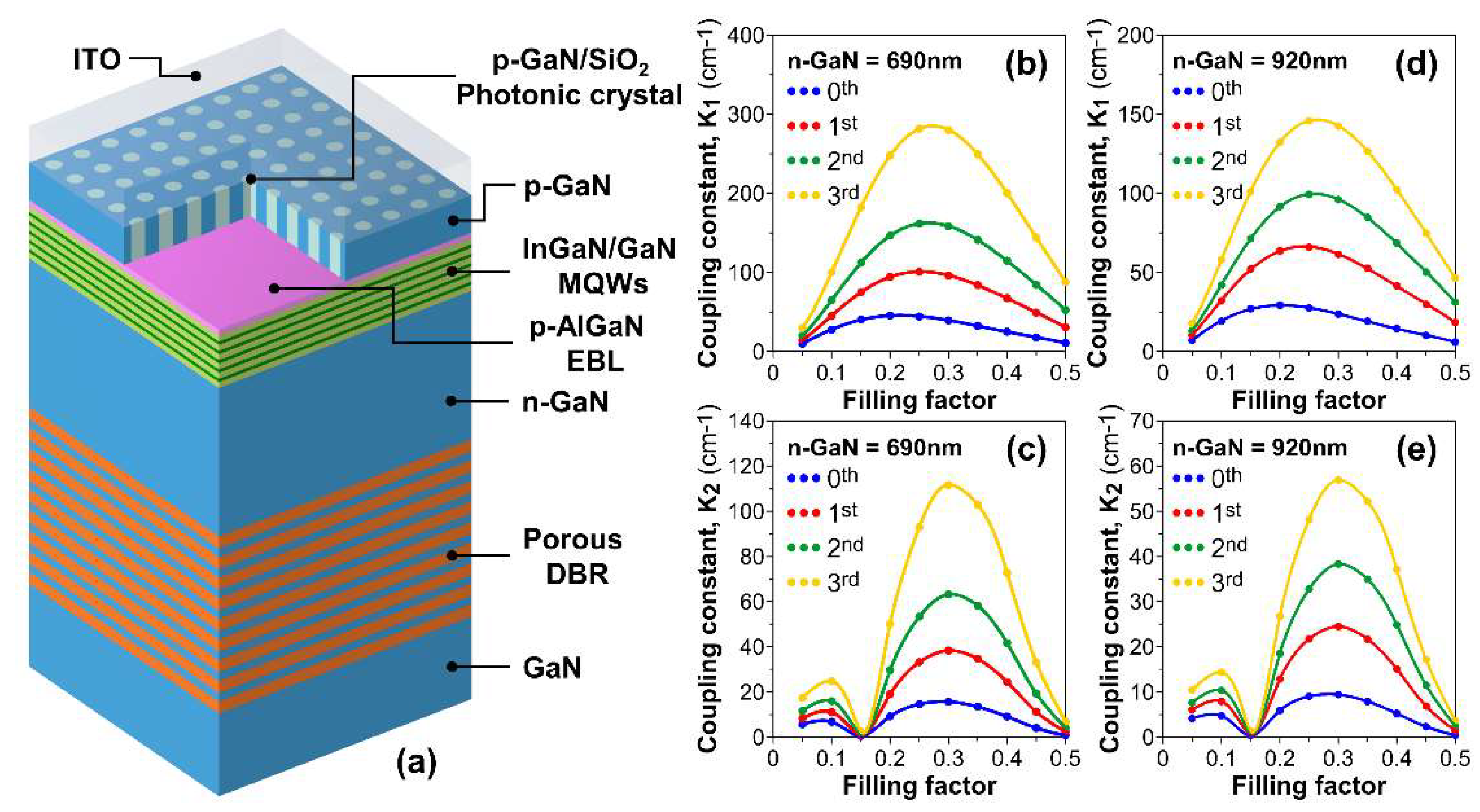
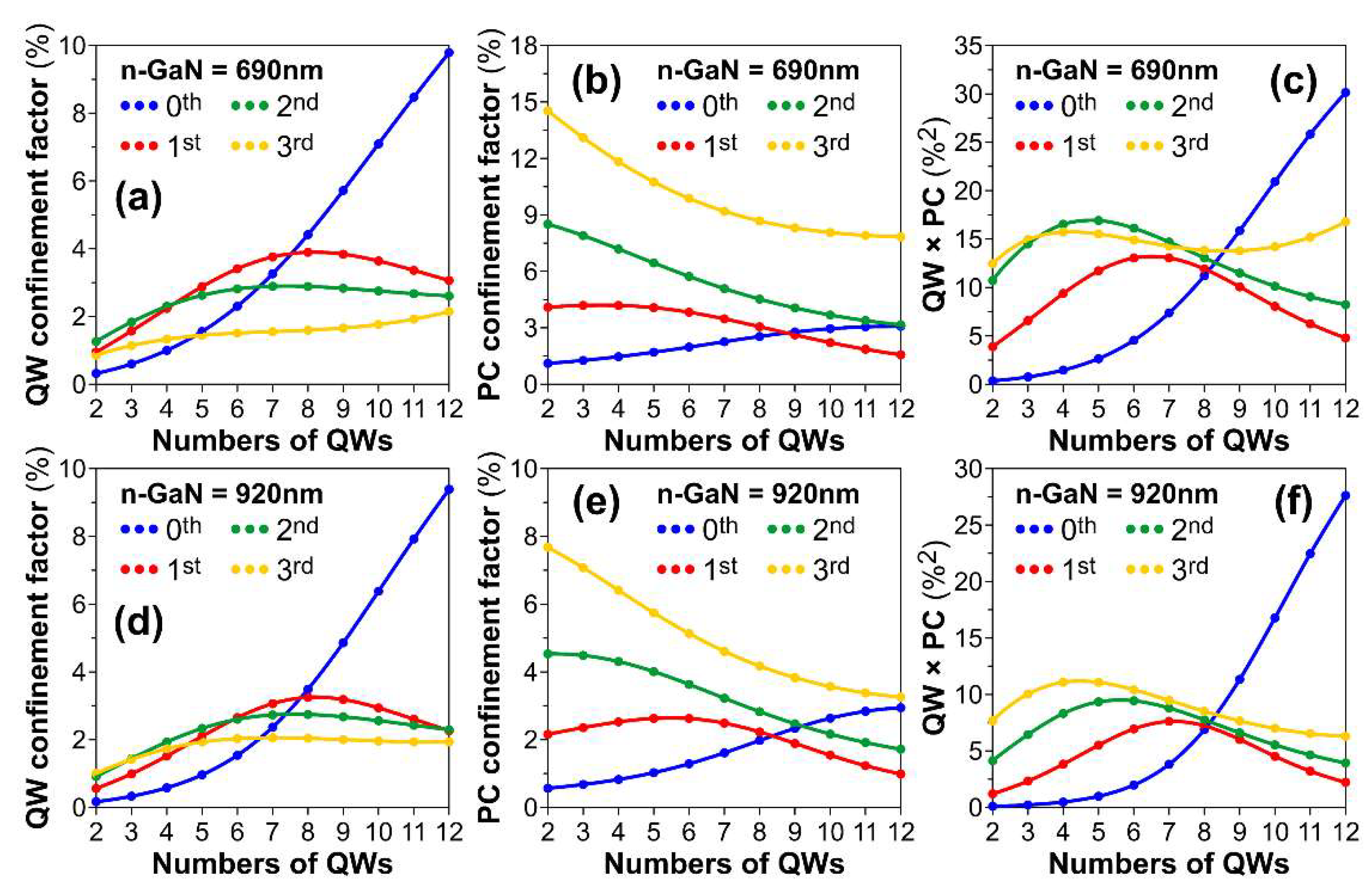
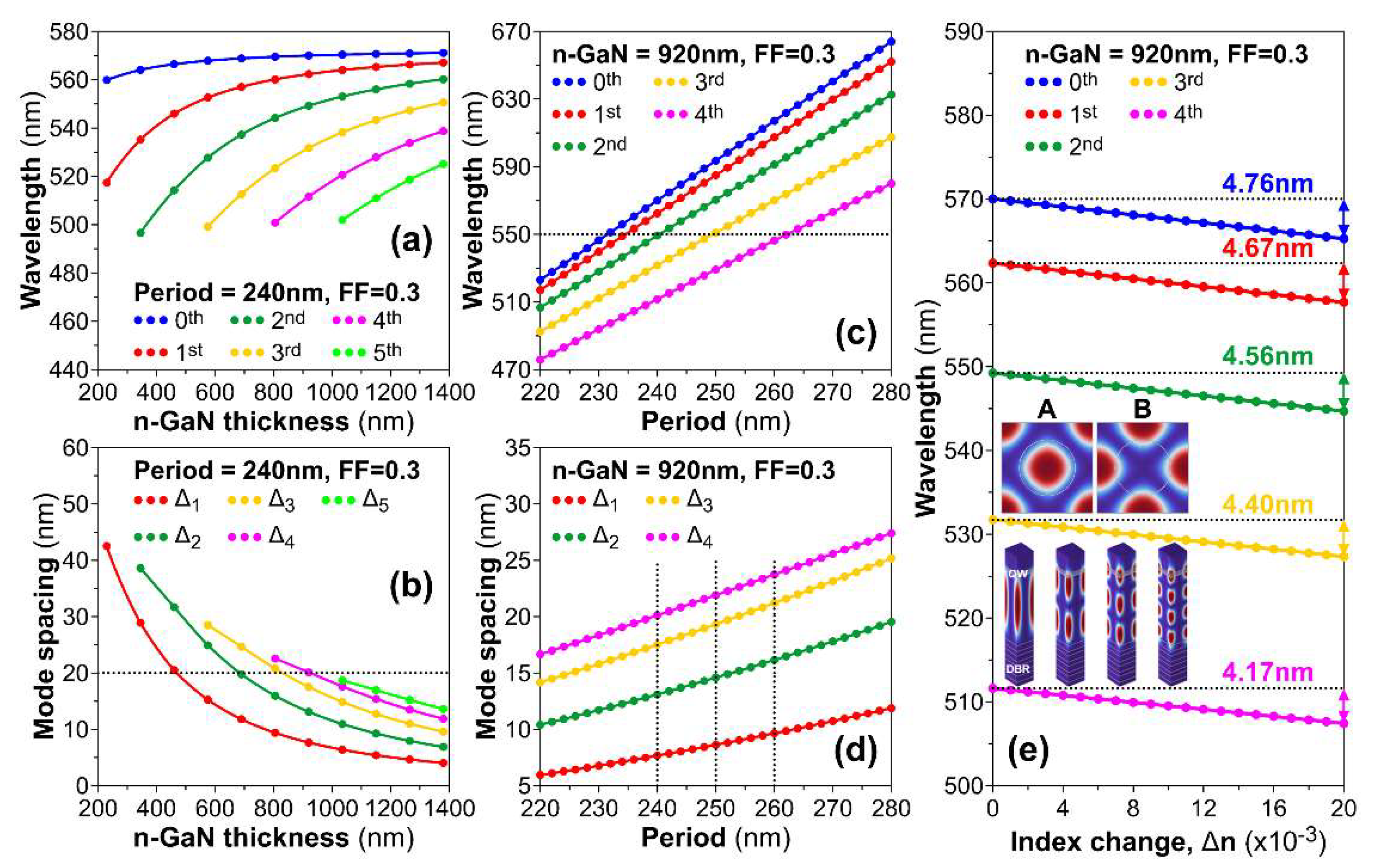
2. Design and Simulation

The primaeval LED wafer structure can be seen in our previous work [37], which was grown on 13 pairs of NP GaN DBR and c-plane GaN substrate. The coupling with NP GaN DBR can increase LEE and decrease the strain-induced quantum-confined Stark effect (QCSE). In this part, we performed systematic numerical analysis to characterize the optical performance of the InGaN-based green (550 nm) µ-PCLED in combination with a 2D p-GaN PC pattern. The three-dimensional (3D) schematic drawing of the proposed InGaN-based green µ-PCLED is shown in Figure 1a. The 2D PC patten is constructed by periodically arranging SiO2 columns (which can also be replaced by other dielectric materials with a lower refractive index, e.g., Al2O3 or SiNx) and surrounding them with p-GaN. The air friction for the NP GaN is estimated to be 0.6. The µ-PCLED unit cell includes InGaN MQWs separated by GaN barriers, a 20 nm thick p-AlGaN electron blocking layer (EBL), a 100 nm thick p-GaN layer and a 100 nm thick indium tin oxide (ITO) layer as the contact layer. The thicknesses of the QWs and barriers were set to be 3 and 10 nm, respectively. To avoid damaging the active layer, the AlGaN EBL can be used as an etching stop layer.
To optimize the filling factor of SiO2, the calculated first- and second-order coupling constants (K1 and K2) of the µ-PCLED containing 5 pairs of InGaN MQWs for n-GaN = 690 nm (~3 λ/n) and 920 nm (~4 λ/n) are shown in Figure 1b–e. The PC period was set to be 232 nm (~λ/n), and circles with different colors indicate the specific orders of FP modes. Here, n = 2.38 for GaN was chosen for the simulation. The FP modes inside the LED are created by the PC and NP DBR. As we can see, the higher-order FP mode leads to the larger first-order (in-plane) and second-order (out-of-plane) Bragg diffraction couplings, because the coupling constants of Bragg diffractions are closely related to the refractive index contrast and confinement factor of the PC [43,44]. Moreover, the highest coupling constants K1 and K2 occur at the filling factor = 0.3 (when the hole’s diameter is about 0.618 times the period), indicating that this specific filling factor of PC is ideal for the µ-PCLED to achieve high output efficiency.
Since optical confinement is an essential parameter for describing the light–matter coupling, the confinement factors of QW and PC as functions of the number of InGaN QWs for n-GaN = 690 nm and 920 nm are shown in Figure 2a,b,d,e, respectively. The QW and PC confinement factors of the fundamental (0th) mode increase with the QW’s number. For the high-order FP modes (1st, 2nd and 3rd), the QW confinement does not increase with the QW’s number regardless of the n-GaN’s thickness. Furthermore, the PC confinement factors gradually decrease as the number of QWs increases. As shown in Figure 2c,f, we used the product of QW confinement factor and PC confinement factor as the figure of merit to optimize the QW’s number. The results reveal that four to six pairs of QWs have the largest products for the 2nd and 3rd FP modes. In addition, the µ-PCLED with the thinner n-GaN also helps to improve the optical confinement.
After optimizing the filling factor and number of QWs, the influences of n-GaN’s thickness and PC’s period on the resonance peaks and mode spacings of the µ-PCLED with 5 pairs of InGaN QWs are shown in Figure 3. Then, the mode wavelength shift induced by the refractive index change (Δn) was also investigated. Based on the fundamental concept of a FP cavity, the number of resonance modes (m ≡ 2ngLeff/λ) and mode spacing (Δλ ≡ λ2/(2ngLeff)) are linearly and inversely proportional to the group index (ng) and cavity length (Leff). The first six hybrid FP modes labelled 0th, 1st, 2nd, 3rd, 4th and 5th for different thicknesses of n-GaN are shown in Figure 3a,b. The symbols Δi in Figure 3b denote the wavelength difference between i-th and (i-1)-th orders of FP modes. In other words, the mode spacing Δi is equal to λi-1–λi. For manufacturing a µ-PCLED with one single-emission peak, the mode spacing Δi should be larger than the full-width at half-maximum (FWHM) of the emission spectrum. To make the Δi greater than 20 nm, the thickness of n-GaN should be smaller than 920 nm.
On the other hand, since the µ-PCLED coupled with the NP GaN DBR forms a hybrid FP cavity, the resonance modes encompass distinctive characteristics of the PC, and the PC mode wavelength is a function of the PC period. The simulated mode profiles of a 3D µ-PCLED unit cell with a 920 nm thick n-GaN layer for the 0th-, 1st-, 2nd- and 3rd-order modes are plotted in the inset of Figure 3e. The symmetrical-mode distributions in vertical and horizontal directions were controlled by the FP cavity and PC structure. The two adjacent PC modes, A and B, near the lowest Γ point of reciprocal space, are also shown in the inset. Mode B would be the better choice to reduce the optical absorption caused by the lossy material (e.g., ITO) filled into the etching holes. Furthermore, the calculated PC mode wavelengths and relevant mode spacings of the µ-PCLED with 5 pairs of QWs and the thickness of n-GaN equal to 920 nm are shown in Figure 3c,d. The calculated wavelengths and spacings are positively correlated with the PC period. According to the simulation results, the desirable periods of the 2nd-, 3rd- and 4th-order modes are about 240 nm (λ = 549.3 nm), 250 nm (λ = 551.1 nm) and 260 nm (λ = 546.3 nm), so that the µ-PCLED can emit green light at around 550 nm. Nevertheless, as shown in Figure 3d, the PC with a sizeable period has a relatively large intermode spacing. Particularly, for the period of 260 nm, the prognosticated mode spacing of 23.7 nm is obviously larger than that for the periods of 240 nm (Δ = 13.1 nm) and 250 nm (Δ = 19.3 nm). Moreover, since the refractive index change is a function of free carrier density [45,46] and the free carrier density could be as high as 1018 to 1020 1/cm3. Δn is estimated to be in the range of 10−3 to 10−2 for the InGaN µ-LED operating at a high injection current density. Therefore, as Δn increases from 0 to 0.02, the calculated mode shifts of FP resonance peaks are approximately 4.2 to 4.8 nm. As suggested by Figure 3e, the PC mode shift in the green spectral region can be lower than 2.5 nm when the refractive index change Δn is less than 0.01. Such a small blue-shift for the µ-PCLED manifests its exceptional wavelength stability.

3. Growth and Fabrication

To construct the InGaN-based green μ-PCLED with the NP GaN DBR, on top of a 2-inch c-plane GaN substrate with a patterned sapphire layer, a 2 μm thick Ge-doped GaN layer was first grown for laying a continuous and high-quality foundation for the following deposition of a 8 μm thick undoped GaN layer. After the epitaxy of the SF-free GaN layer, the wafer was planarized by chemical mechanical polishing (CMP). Subsequently, 13 pairs of NP n-GaN/undoped GaN DBR were fabricated, followed by the formation of a near-1 µm-thick n-GaN layer and five pairs of InGaN (3 nm)/GaN (10 nm) MQWs as the active layer. The NP n-GaN layers were fabricated through the following steps: (1) constructing indium contacts on the n-GaN surface, (2) immersing the n-GaN layers and platinum targets into the acid solution, (3) applying a forward voltage of 8V, (4) cleaning the finished NP GaN layer in deionized water and (5) blowing dry with N2 gas.
Next, a 20 nm thick p-AlGaN EBL and a 100 nm thick p-GaN PC layer were grown on the active layer. The detailed fabrication process without the PC layer can be found in our earlier publication [37]. Regarding the 2D PC structure, the circular holes were first defined by electron-beam lithography and then etched through the p-GaN layer. The etching stopped at the top surface of the p-AlGaN layer. The diameter of approximately 161 nm and period of 260 nm for the air holes were determined by the simulations. Then, a 10 nm thick Al2O3 layer was deposited on the surfaces of the air holes by atomic layer deposition (ALD) for passivation. The detailed fabrication process for the p-GaN PC layer can be found in our previous publications [19,47,48]. After that, the SiO2 layer was also deposited into the etched holes, followed by multiple rounds of SiO2 etching back processes to expose the p-GaN surface.
Finally, a 100 nm thick ITO layer was deposited by electron-beam physical vapor deposition (EB-PVD) on the p-GaN PC surface. The mesa with a diameter of 30 μm and depth of 1 μm for the μ-PCLED was etched by using the HCl solution for ITO and the ICP-RIE for GaN sequentially. Thereafter, the Ti (20 nm)/Al (100 nm)/Ni (45 nm)/Au (55 nm) metal ohmic contact metal layer was deposited on the ITO layer as the electrodes.

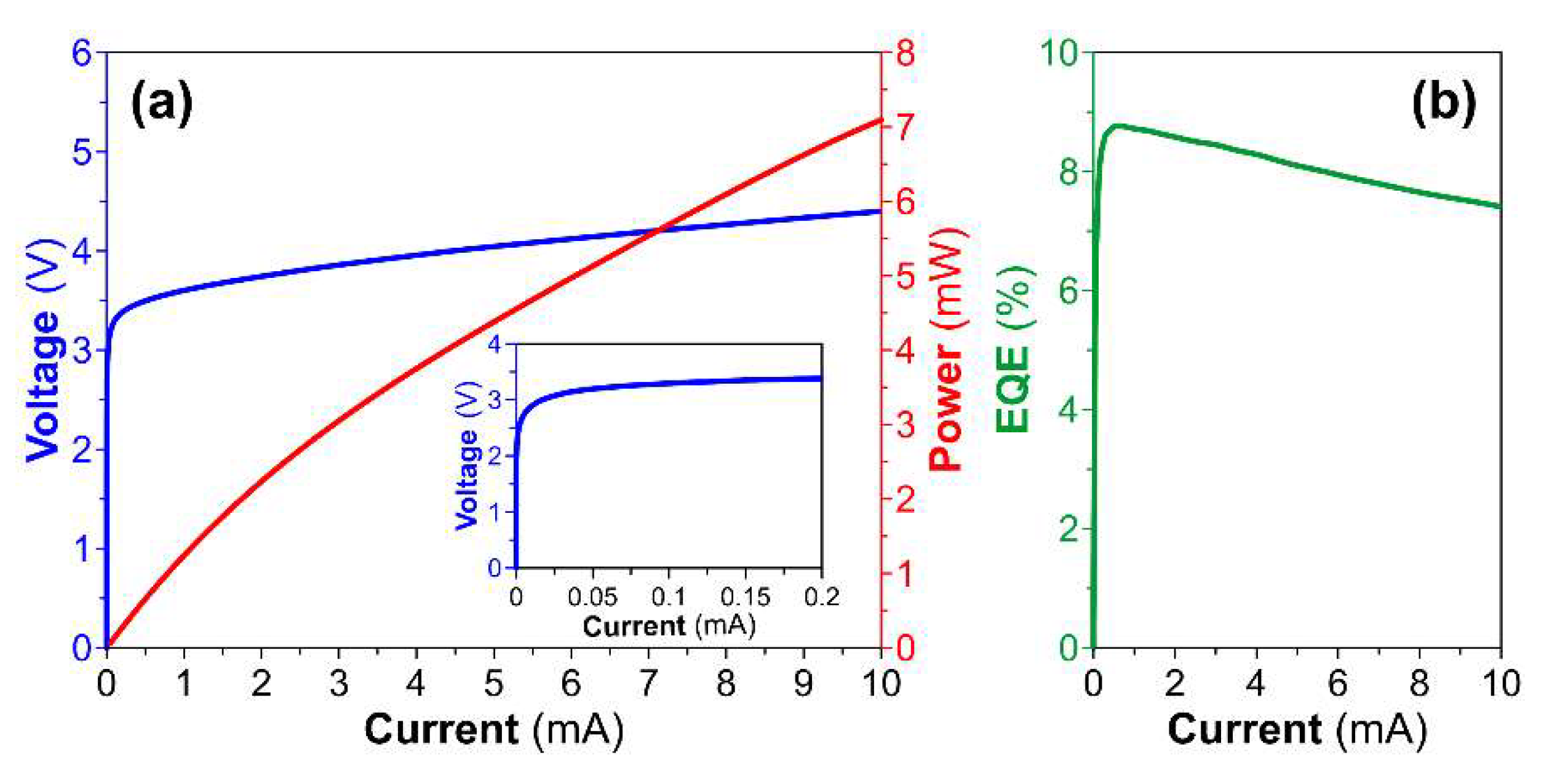
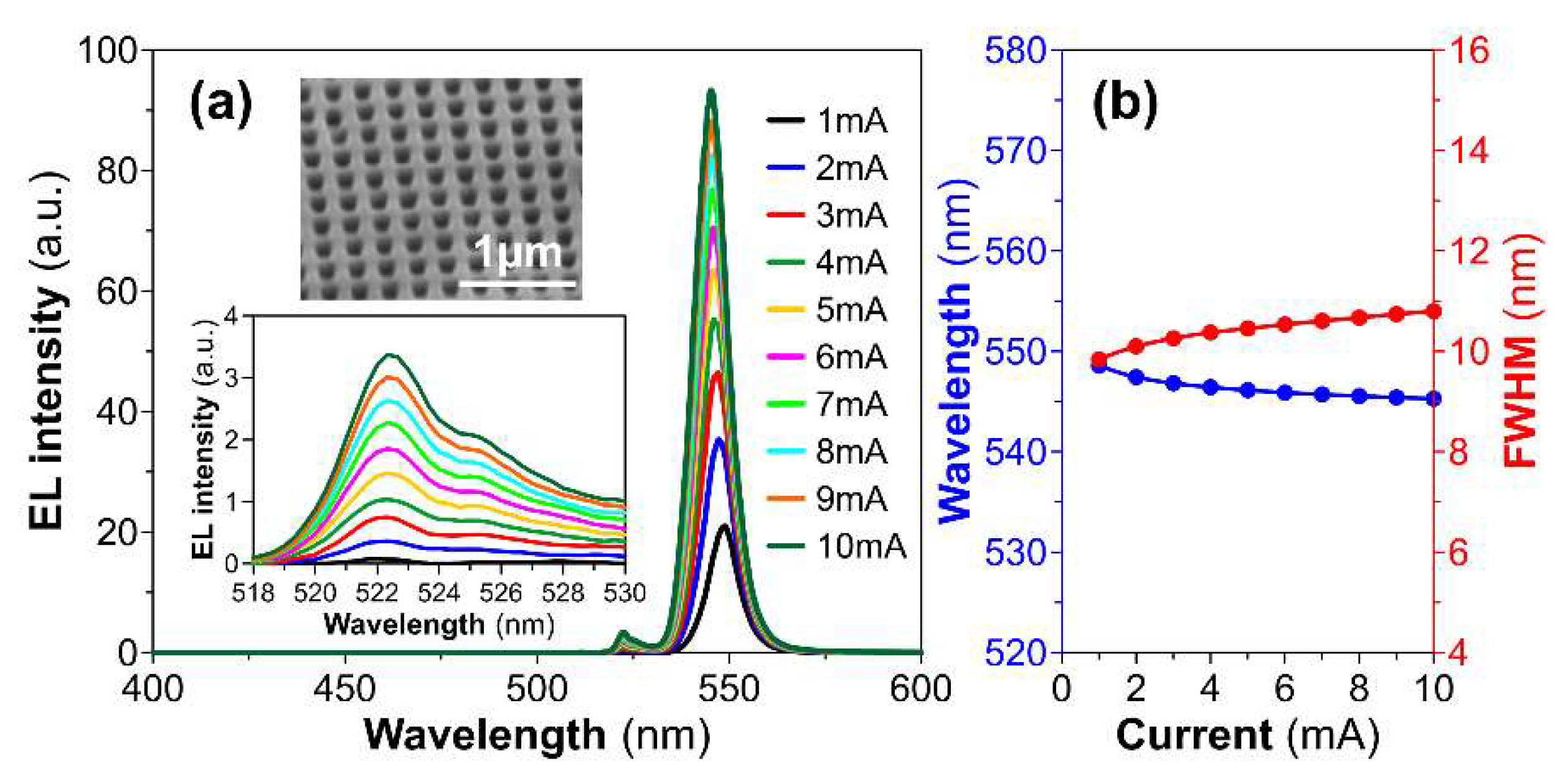
4. Results and Discussion

The electrical and optical properties of the fabricated green µ-PCLED with the bottom NP GaN DBR are summarized in Figure 4 and Figure 5. Figure 4a shows the measured light–current–voltage (L-I-V) curve, indicating the turn-on voltage of about 2.7 V. In addition, the maximum EQE of the fabricated green μ-PCLED is approximately 8.8% at a low injection current of 0.73 mA, as shown in Figure 4b. However, when the injection current is higher than 0.73 mA, the efficiency droop becomes obvious due to the QCSE. Compared to conventional ones, here the µ-PCLED exhibits a relatively small efficiency drop because the epitaxial strain is alleviated by the application of NP DBRs [37].
Figure 5a illustrates the current-dependent electroluminescence spectra of the µ-PCLED with the bottom NP DBR. The inset in Figure 5a shows the SEM image of the p-GaN PC. The green µ-PCLED with single mode emission and narrow FWHM was realized. The measured emission peak slowly moves to shorter wavelengths as the injection current increases from 1 to 10 mA. The measured emission peak and FWHM as a function of injection current are characterized in Figure 5b, indicating that the central wavelength of the electroluminescence spectrum shifts from 548.5 to 545.3 nm. At the same time, the measured FWHM changes from about 9.8 to 10.8 nm. In comparison, a blue shift of 6 nm and an average FWHM of 27 nm for the green µ-LEDs with sizes of 47 × 47 µm2 and 98 × 98 µm2 at low current densities were demonstrated in [36]. In addition, InGaN-based green µ-LEDs with the diameter of 40 μm showed blue-shifts of around 12 nm [49] and 19 nm [50]. Similarly, the green µ-LEDs with the diameters of 1 to 20 μm showed an insignificant dependence of size on the blue-shift of about 15 nm [51]. Moreover, the literature showed the blue-shifts in wavelength for the semi-polar (11–22) and c-plane green µ-LEDs were 5 and 16 nm, respectively [52]. Such a µ-PCLED with slight blue-shift and narrow FWHM demonstrated superior color saturation compared to the literature [23,53,54]. It is worth mentioning that insignificant minor peaks seem to appear with a Fabry–Perot mode spacing from the major peak larger than 20 nm, as shown in Figure 5a. In summary, the measurement results are in good agreement with the numerical simulation results, indicating that our design is reliable for the development of μ-PCLEDs.

5. Conclusions

We numerically and experimentally investigated the optoelectronic characteristics of an InGaN-based green µ-PCLED with a NP GaN DBR. Numerical simulations for the 3D µ-PCLED unit cell model were performed by using a finite element method. The influences of structural parameters, including the etching hole’s filling factor, PC’s period, QW’s number, n-GaN’s thickness and refractive index change, on the optical characteristics of the µ-PCLED, were systematically explored. The simulation results revealed that the green µ-PCLED with a filling factor of 0.3 achieved the most efficient in-plane and out-of-plane Bragg diffraction couplings. Based on the figure of merit, which is defined as the product of the QW and PC confinement factors, the µ-PCLED with four to six pairs of InGaN QWs is the preferable design for simultaneously obtaining high optical confinement and high coupling constant. In addition, for a FP cavity, the thickness of n-GaN is controlled to be less than 920 nm for realizing a mode spacing of lager than 20 nm. The calculated mode shift of the resonance modes generated by the µ-PCLED integrated with the NP GaN DBR is small enough to suppress the blue-shift, even with large refractive index change. Accordingly, the measurement results show that the fabricated µ-PCLED indeed emits 545 nm green light, for the injection current ranging from 1 to 10 mA. At the same time, the peak wavelength blue-shift is approximately equal to 3 nm. In general, the measurement results, especially the emission peak wavelengths and FMHMs, are consistent with the simulation results. The green µ-PCLED design proposed in this work may offer a foundation for further investigation of the next-generation light source.

Author Contributions

Conceptualization, H.-C.K.; methodology, K.-B.H., W.-T.H. and W.-C.H.; investigation, K.-B.H., C.-C.T. and H.-C.K.; device preparation, W.-T.H. and W.-C.H.; experimental measurements, W.-T.H. and W.-C.H.; validation, K.-B.H., W.-T.H., W.-C.H. and C.-C.T.; writing—original draft preparation, K.-B.H. and W.-T.H.; writing—review and editing, K.-B.H., C.-C.T. and H.-C.K. supervision, H.-C.K. All authors have read and agreed to the published version of the manuscript.

Funding

This research was funded by the Ministry of Science and Technology in Taiwan (Grant Nos. MOST 110-2622-8-A49-008-SB).

Institutional Review Board Statement

Not applicable.

Informed Consent Statement

Not applicable.

Data Availability Statement

Not applicable.

Acknowledgments

The authors express their gratitude to the Hon Hai Research Institute for their technical support and helpful discussion.

Conflicts of Interest

The authors declare no conflict of interest.

References

  1. Park, S.I.; Xiong, Y.; Kim, R.H.; Elvikis, P.; Meitl, M.; Kim, D.H.; Wu, J.; Yoon, J.; Yu, C.J.; Liu, Z.; et al. Printed assemblies of inorganic light-emitting diodes for deformable and semitransparent display. Science 2009, 325, 977–981. [Google Scholar] [CrossRef] [PubMed] [Green Version]
  2. Jiang, Y.; Li, Y.; Li, Y.; Deng, Z.; Lu, T.; Ma, Z.; Zuo, P.; Dai, L.; Wang, L.; Jia, H.; et al. Realization of high-luminous-efficiency InGaN light-emitting diodes in the “green gap” range. Sci. Rep. 2015, 5, 10883. [Google Scholar] [CrossRef] [PubMed] [Green Version]
  3. Liu, X.; Lin, R.; Chen, H.; Zhang, S.; Qian, Z.; Zhou, G.; Chen, X.; Zhou, X.; Zheng, L.; Liu, R.; et al. High-bandwidth InGaN self-powered detector arrays toward MIMO visible light communication based on micro-LED arrays. ACS Photonics 2019, 6, 3186–3195. [Google Scholar] [CrossRef]
  4. Haas, H. LiFi is a paradigm-shifting 5G technology. Rev. Phys. 2018, 3, 26–31. [Google Scholar] [CrossRef]
  5. Bergh, A.A. Blue laser diode (LD) and light emitting diode (LED) applications. Phys. Stat. Sol. 2004, 201, 2740–2754. [Google Scholar]
  6. Taniyasu, Y.; Kasu, M.; Makimoto, T. An aluminium nitride light-emitting diode with a wavelength of 210 nanometres. Nature 2006, 441, 325–328. [Google Scholar] [CrossRef]
  7. Zhan, T.; Yin, K.; Xiong, J.; He, Z.; Wu, S.T. Augmented reality and virtual reality displays: Perspectives and challenges. iScience 2020, 23, 101397. [Google Scholar] [CrossRef]
  8. Huang, Y.; Hsiang, E.L.; Deng, M.Y.; Wu, S.T. Mini-LED, micro-LED and OLED displays: Present status and future perspectives. Light Sci. Appl. 2020, 9, 105. [Google Scholar] [CrossRef]
  9. Xiong, J.; Hsiang, E.L.; He, Z.; Zhan, T.; Wu, S.T. Augmented reality and virtual reality displays: Emerging technologies and future perspectives. Light Sci. Appl. 2021, 10, 216. [Google Scholar] [CrossRef]
  10. Liu, Z.; Lin, C.-H.; Hyun, B.-R.; Sher, C.-W.; Lv, Z.; Luo, B.; Jiang, F.; Wu, T.; Ho, C.-H.; Kuo, H.-C.; et al. Micro-light-emitting diodes with quantum dots in display technology. Light Sci. Appl. 2020, 9, 83. [Google Scholar] [CrossRef]
  11. Hsiang, E.-L.; He, Z.; Huang, Y.; Gou, F.; Lan, Y.-F.; Wu, S.-T. Improving the Power Efficiency of Micro-LED Displays with Optimized LED Chip Sizes. Crystals 2020, 10, 494. [Google Scholar] [CrossRef]
  12. Huang, H.-W.; Chu, J.T.; Kao, C.C.; Hseuh, T.H.; Lu, T.C.; Kuo, H.C.; Wang, S.C.; Yu, C.C. Enhanced light output of an InGaN/GaN light emitting diode with a nano-roughened p-GaN surface. Nanotechnology 2005, 16, 1844. [Google Scholar] [CrossRef] [Green Version]
  13. Ee, Y.-K.; Kumnorkaew, P.; Arif, R.A.; Tong, H.; Gilchrist, J.F.; Tansu, N. Light extraction efficiency enhancement of InGaN quantum wells light-emitting diodes with polydimethylsiloxane concave microstructures. Opt. Express 2009, 17, 13747–13757. [Google Scholar] [CrossRef] [Green Version]
  14. Denbaars, S.P.; Feezell, D.; Kelchner, K.; Pimputkar, S.; Pan, C.C.; Yen, C.C.; Tanaka, S.; Zhao, Y.; Pfaff, N.; Farrell, R.; et al. Development of gallium-nitride-based light-emitting diodes (LEDs) and laser diodes for energy-efficient lighting and displays. Acta Mater. 2013, 61, 945–951. [Google Scholar] [CrossRef]
  15. David, A. Surface-Roughened Light-Emitting Diodes: An Accurate Model. J. Display Technol. 2013, 9, 301–316. [Google Scholar] [CrossRef]
  16. Kim, J.Y.; Kwon, M.K.; Lee, K.S.; Park, S.J. Enhanced light extraction from GaN-based green light-emitting diode with photonic crystal. Appl. Phys. Lett. 2007, 91, 181109. [Google Scholar] [CrossRef]
  17. Xu, Z.; Cao, L.; Tan, Q.; He, Q.; Jin, G. Enhancement of the light output of light-emitting diode with double photonic crystals. Opt. Commun. 2007, 278, 211–214. [Google Scholar] [CrossRef]
  18. Cheng, B.S.; Chiu, C.H.; Huang, K.J.; Lai, C.F.; Kuo, H.C.; Lin, C.H.; Lu, T.C.; Wang, S.C.; Yu, C.C. Enhanced light extraction of InGaN-based green LEDs by nano-imprinted 2D photonic crystal pattern. Semicond. Sci. Technol. 2008, 23, 055002. [Google Scholar] [CrossRef] [Green Version]
  19. Lai, C.F.; Chao, C.H.; Kuo, H.C.; Yen, H.H.; Lee, C.E.; Yeh, W.Y. Directional light extraction enhancement from GaN-based film-transferred photonic crystal light-emitting diodes. Appl. Phys. Lett. 2009, 94, 123106. [Google Scholar] [CrossRef] [Green Version]
  20. Wierer, J.; David, A.; Megens, M. III-nitride photonic-crystal light-emitting diodes with high extraction efficiency. Nature Photon. 2009, 3, 163–169. [Google Scholar] [CrossRef]
  21. Kim, J.Y.; Kwon, M.K.; Park, S.J.; Kim, S.H.; Lee, K.D. Enhancement of light extraction from GaN-based green light-emitting diodes using selective area photonic crystal. Appl. Phys. Lett. 2010, 96, 251103. [Google Scholar] [CrossRef]
  22. Chang, Y.C.; Liou, J.K.; Liu, W.C. Improved light extraction efficiency of a high-power GaN-based light-emitting diode with a three-dimensional-photonic crystal (3-D-PhC) backside reflector. IEEE Electron Device Lett. 2013, 34, 777–779. [Google Scholar] [CrossRef]
  23. Yin, Y.F.; Lan, W.Y.; Lin, T.C.; Wang, C.; Feng, M.; Huang, J.J. High-speed visible light communication using GaN-based light-emitting diodes with photonic crystals. J. Light. Technol. 2017, 35, 258–264. [Google Scholar] [CrossRef]
  24. Schubert, E.F.; Wang, Y.H.; Cho, A.Y.; Tu, L.W.; Zydzik, G.J. Resonant cavity light-emitting diode. Appl. Phys. Lett. 1992, 60, 921. [Google Scholar] [CrossRef]
  25. Pessa, M.; Guina, M.; Dumitrescu, M.; Hirvonen, I.; Saarinen, M.; Toikkanen, L.; Xiang, N. Resonant cavity light emitting diode for a polymer optical fibre system. Semicond. Sci. Technol. 2002, 17, R1. [Google Scholar] [CrossRef]
  26. Delbeke, D.; Bockstaele, R.; Bienstman, P.; Baets, R.; Benisty, H. High-Efficiency Semiconductor Resonant-Cavity Light-Emitting Diodes: A Review. IEEE J. Sel. Top. Quantum Electron. 2002, 8, 189–206. [Google Scholar] [CrossRef]
  27. Byrne, D.; Natali, F.; Damilano, B.; Dussaigne, A.; Grandjean, N.; Massies, J. Blue resonant cavity light emitting diodes with a high-Al-content GaN/AlGaN distributed Bragg reflector. Jpn. J. Appl. Phys. 2003, 42, L1509. [Google Scholar] [CrossRef]
  28. Shiu, G.Y.; Chen, K.T.; Fan, F.H.; Huang, K.P.; Hsu, W.J.; Dai, J.J.; Lai, C.F.; Lin, C.F. InGaN Light-Emitting Diodes with an Embedded Nanoporous GaN Distributed Bragg Reflectors. Sci. Rep. 2016, 6, 29138. [Google Scholar] [CrossRef] [Green Version]
  29. Ryu, H.-Y.; Hwang, J.-K.; Lee, Y.-J.; Lee, Y.-H. Enhancement of light extraction from two-dimensional photonic crystal slab structures. J. Sel. Top. Quantum Electron. 2002, 8, 231–237. [Google Scholar]
  30. Shin, Y.C.; Kim, D.H.; Kim, E.H.; Park, J.M.; Ho, K.M.; Constant, K.; Choe, J.H.; Park, Q.H.; Ryu, H.Y.; Baek, J.H.; et al. High efficiency GaN light-emitting diodes with two dimensional photonic crystal Structures of deep-hole square lattices. IEEE J. Quantum Electron. 2010, 46, 116–120. [Google Scholar] [CrossRef]
  31. Yamamoto, S.; Zhao, Y.; Pan, C.C.; Chung, R.B.; Fujito, K.; Sonoda, J.; DenBaars, S.P.; Nakamura, S. High-efficiency single-quantum-well green and yellow-green light-emitting diodes on semipolar (2021) GaN substrates. Appl. Phys. Express 2010, 3, 122102. [Google Scholar] [CrossRef]
  32. Iida, D.; Niwa, K.; Kamiyama, S.; Ohkawa, K. Demonstration of InGaN-based orange LEDs with hybrid multiple-quantum-wells structure. Appl. Phys. Express 2016, 9, 111003. [Google Scholar] [CrossRef]
  33. Iida, D.; Lu, S.; Hirahara, S.; Niwa, K.; Kamiyama, S.; Ohkawa, K. Enhanced light output power of InGaN-based amber LEDs by strain-compensating AlN/AlGaN barriers. J. Cryst. Growth 2016, 448, 105–108. [Google Scholar] [CrossRef]
  34. Hu, H.; Zhou, S.; Wan, H.; Liu, X.; Li, N.; Xu, H. Effect of strain relaxation on performance of InGaN/GaN green LEDs grown on 4-inch sapphire substrate with sputtered AlN nucleation layer. Sci. Rep. 2019, 9, 3447. [Google Scholar] [CrossRef] [PubMed] [Green Version]
  35. Zhuang, Z.; Iida, D.; Velazquez-Rizo, M.; Ohkawa, K. 606-nm InGaN amber micro-light-emitting diodes with an on-wafer external quantum efficiency of 0.56%. IEEE Electron Device Lett. 2021, 42, 1029–1032. [Google Scholar] [CrossRef]
  36. Zhuang, Z.; Iida, D.; Ohkawa, K. Investigation of InGaN-based red/green micro-light-emitting diodes. Opt. Lett. 2021, 46, 1912–1915. [Google Scholar] [CrossRef]
  37. Huang, W.T.; Peng, C.Y.; Chiang, H.; Huang, Y.M.; Singh, K.J.; Lee, W.B.; Chow, C.W.; Chen, S.C.; Kuo, H.C. Toward high-bandwidth yellow-green micro-LEDs utilizing nanoporous distributed Bragg reflectors for visible light communication. Photon. Res. 2022, 10, 1810–1818. [Google Scholar] [CrossRef]
  38. Gonga, Z.; Jin, S.; Chen, Y.; McKendry, J.; Massoubre, D.; Watson, I.M.; Gu, E.; Dawson, M.D. Size-dependent light output, spectral shift, and self-heating of 400 nm InGaN light-emitting diodes. J. Appl. Phys. 2010, 107, 013103. [Google Scholar] [CrossRef]
  39. Guo, Q.; Li, D.; Hua, Q.; Ji, K.; Sun, W.; Hu, W.; Wang, Z.L. Enhanced Heat Dissipation in Gallium Nitride-Based Light-Emitting Diodes by Piezo-phototronic Effect. Nano Lett. 2021, 21, 4062–4070. [Google Scholar] [CrossRef]
  40. Alaei, S.; Seifouri, M.; Babaabbasi, G.; Olyaee, S. Numerical investigation on self-heating effect in 1.3 µm quantum dot photonic crystal microstructure VCSELs. Eur. Phys. J. Plus 2022, 137, 515. [Google Scholar] [CrossRef]
  41. Rashidi, A.; Monavarian, M.; Aragon, A.; Feezell, D. Thermal and efficiency droop in InGaN/GaN light-emitting diodes: Decoupling Multiphysics effects using temperature-dependent RF measurements. Sci. Rep. 2019, 9, 19921. [Google Scholar] [CrossRef] [PubMed] [Green Version]
  42. Zhang, Y.; Lu, S.; Qiu, Y.; Wu, J.; Zhang, M.; Luo, D. Experimental and Modeling Investigations of Miniaturization in InGaN/GaN Light-Emitting Diodes and Performance Enhancement by Micro-Wall Architecture. Front. Chem. 2021, 8, 2296–2646. [Google Scholar] [CrossRef] [PubMed]
  43. Streifer, W.; Scifres, D.; Burnham, R. Coupled wave analysis of DFB and DBR lasers. IEEE J. Quantum Electron. 1977, 13, 134–141. [Google Scholar] [CrossRef]
  44. Wiesmann, D.; Germann, R.; Bona, G.L. Add–drop filter based on apodized surface-corrugated gratings. J. Opt. Soc. Am. B 2003, 20, 417–423. [Google Scholar] [CrossRef]
  45. Jiang, H.X.; Lin, J.Y. Mode spacing ‘‘anomaly’’ in InGaN blue lasers. Appl. Phys. Lett. 1999, 74, 1066–1068. [Google Scholar] [CrossRef]
  46. de Arriba, G.M.; Feng, P.; Xu, C.; Zhu, C.; Bai, J.; Wang, T. Simple approach to mitigate the emission wavelength instability of III-Nitride μLED Arrays. ACS Photonics 2022, 9, 2073–2078. [Google Scholar] [CrossRef]
  47. Lai, C.F.; Kuo, H.C.; Chao, C.H.; Yu, P.; Yeh, W.Y. Structural effects on highly directional far-field emission patterns of GaN-based micro-cavity light-emitting diodes with photonic crystals. J. Light. Technol. 2010, 28, 2881–2889. [Google Scholar] [CrossRef]
  48. Lai, C.F.; Kuo, H.C.; Yu, P.; Lu, T.C.; Chao, C.H.; Yen, H.H.; Yeh, W.Y. Highly-directional emission patterns based on near single guided mode extraction from GaN-based ultrathin microcavity light-emitting diodes with photonic crystals. Appl. Phys. Lett. 2010, 97, 013108. [Google Scholar] [CrossRef]
  49. Wu, Y.; Liu, B.; Xu, F.; Sang, Y.; Tao, T.; Xie, Z.; Wang, K.; Xiu, X.; Chen, P.; Chen, D.; et al. High-efficiency green micro-LEDs with GaN tunnel junctions grown hybrid by PA-MBE and MOCVD. Photon. Res. 2021, 9, 1683–1688. [Google Scholar] [CrossRef]
  50. Wang, Z.; Zhu, S.; Shan, X.; Yuan, Z.; Qian, Z.; Lu, X.; Fu, Y.; Tu, K.; Guan, H.; Cui, X.; et al. Red, green and blue InGaN micro-LEDs for display application: Temperature and current density effects. Opt. Express 2022, 30, 36403–36413. [Google Scholar] [CrossRef]
  51. Yu, L.; Lu, B.; Yu, P.; Wang, Y.; Ding, G.; Feng, Q.; Jiang, Y.; Chen, H.; Huang, K.; Hao, Z.; et al. Ultra-small size (1–20 μm) blue and green micro-LEDs fabricated by laser direct writing lithography. Appl. Phys. Lett. 2022, 121, 042106. [Google Scholar] [CrossRef]
  52. Li, H.; Wong, M.S.; Khoury, M.; Bonef, B.; Zhang, H.; Chow, Y.; Li, P.; Kearns, J.; Taylor, A.A.; Mierry, P.D.; et al. Study of efficient semipolar (11-22) InGaN green micro-light-emitting diodes on highquality (11–22) GaN/sapphire template. Opt. Express 2019, 27, 24154–24160. [Google Scholar] [CrossRef] [PubMed]
  53. Wei, T.; Huo, Z.; Zhang, Y.; Zheng, H.; Chen, Y.; Yang, J.; Hu, Q.; Duan, R.; Wang, J.; Zeng, Y.; et al. Efficiency enhancement of homoepitaxial InGaN/GaN light-emitting diodes on freestanding GaN substrate with double embedded SiO2 photonic crystals. Opt. Express 2014, 22, A1093–A1100. [Google Scholar] [CrossRef] [PubMed]
  54. Jiang, S.; Feng, Y.; Chen, Z.; Zhang, L.; Jiang, X.; Jiao, Q.; Li, J.; Chen, Y.; Li, D.; Liu, L.; et al. Study on light extraction from GaN-based green light-emitting diodes using anodic aluminum oxide pattern and nanoimprint lithography. Sci. Rep. 2016, 6, 21573. [Google Scholar] [CrossRef] [PubMed]
Figure 1. (a) Schematic of the InGaN-based µ-PCLED incorporated with the NP GaN DBR. (b,c) and (d,e) First- and second-order coupling constants of the µ-PCLED with n-GaN = 690 nm and 920 nm as a function of the filling factor. The PC period was set to 232 nm. Circles with different colors indicate the specific orders of FP modes.
Photonics 09 00939 g001
Figure 2. (a,b) Calculated QW and PC confinement factors of the µ-PCLED with n-GaN = 690 nm for different numbers of QWs. (c) Product of QW and PC confinement factors with n-GaN = 690 nm. (d,e) Calculated QW and PC confinement factors of the µ-PCLED with n-GaN = 690 nm for different numbers of QWs. (f) Products of QW and PC confinement factors with n-GaN = 920 nm. The PC period and filling factor for the above calculations were set to 232 nm and 0.3.
Photonics 09 00939 g002
Figure 3. (a) FP resonance wavelength as a function of the n-GaN thickness of the µ-PCLED with 5 pairs of QWs. (b) Mode spacing of adjacent FP peaks extracted from (a). (c,d) FP resonance wavelength and corresponding mode spacing as a function of the PC period of the µ-PCLED with 5 pairs of QWs and n-GaN = 920 nm. (e) FP resonance wavelength shift as a function of the refractive index change in the µ-PCLED with n-GaN = 920 nm. The PC period and filling factor for the calculation were set to be 240 nm and 0.3. The upper inset shows the top views of two fundamental PC mode profiles labeled by A and B. The vertical-mode profiles of the PC mode A for the 0th-, 1st-, 2nd- and 3rd-order modes are shown in the lower inset.
Photonics 09 00939 g003
Figure 4. (a) Measured light–current–voltage curve and (b) external quantum efficiency of the fabricated InGaN-based green µ-PCLED with a mesa diameter of 30 µm. The inset in Figure 4a shows the zoom-in picture of I-V curve.
Photonics 09 00939 g004
Figure 5. (a) Measured electroluminescence spectra for the injection current increases from 1 to 10 mA. (b) Current-dependent peak wavelengths and FWHMs of the fabricated green µ-PCLED with a mesa diameter of 30 µm. The insets in Figure 5a show the SEM image of the p-GaN PC and zoom-in picture of spectra for minor peaks.
Photonics 09 00939 g005
Publisher’s Note: MDPI stays neutral with regard to jurisdictional claims in published maps and institutional affiliations.

