1. Introduction
The electromagnetic spectrum (EMS) is a critically important resource in commercial wireless communication and modern electronic warfare [
1]. Therefore, electric field sensors are vital to detect the EMS parameters such as frequency, power, and waveform. As the EMS becomes congested, EM apparatuses such as radars are evolving towards high-frequency bands. Hence, broadband electric field sensors are urgently needed. In addition, to improve portability and concealment capability, electric field sensors should be small size in and without electromagnetic wave emission [
2].
A variety of electric field sensors have been developed in past years. Traditional broadband electric field sensors are commercially available at present. The typical product is the series of Narda-NBM-550, whose operation frequency range is from 300 MHz to 50 GHz. Nevertheless, the output is a direct current (DC) voltage corresponding to the amplitude of the electric field, where the frequency domain and the time domain information of the signal are missing. D-dot type electric field sensors have been extensively studied in recent years because of their ability to achieve high-power sensing in the operation bandwidth up to 10 GHz [
3,
4,
5,
6]. However, the D-dot-type sensors generally have a large size up to tens of centimeters. As an alternative, photonic EMS sensors have been widely developed, which have both s small size and a relatively broad operation bandwidth [
7,
8,
9,
10]. The electric field sensor, based on electro-optic modulation by Pockels effect on lithium niobate (LN), is one kind of passive optical device without electromagnetic wave emission. This type also has a superior performance in operation bandwidth, sensitivity, dynamic range and linearity compared with the devices fabricated by using other materials. The modulated optical wave can propagate through a long optical fiber with ultra-low transmission loss and without electromagnetic interference, which is beneficial for achieving remote sensing with a high fidelity. Generally, the LN-based electric field sensor has a small size down to several centimeters. Due to the abundant design free degree of the waveguides and the antennas, a variety of LN-based electric field sensors are proposed for diverse electromagnetic sensing applications [
11,
12,
13,
14,
15,
16]. These works are mainly concentrated on the operation bandwidth and the sensitivity of the sensor. For example, the LN sensor based on a Mach–Zehnder interferometer, reached an operation frequency range of 10 kHz to 18 GHz [
11]. The thin film LN sensor, based on a Michelson interferometer, realized a sensitivity of 8.45 mV/m/Hz
−1/2 [
16].
In this paper, broadband and remote EMS sensing is proposed and demonstrated using an LN-based photonic electric field sensor chip with a length of 3.8 cm and a width of 1 cm. The sensor chip is fabricated based on an asymmetrical Mach–Zehnder interferometer (AMZI), whose transmission point is controlled by tuning the wavelength of the optical carrier. Hence, it is free of an electric power supply, which is beneficial for achieving remote sensing. In the experiment, the operation bandwidth of the electric field sensor chip is measured to be over 26.5 GHz in a transverse electric and magnetic (TEM) cell and an anechoic chamber. By using this sensor chip, on–off keying (OOK) signals with an amplitude of 133 V/m, a center frequency of 3 GHz and baseband rates from 1 Mb/s to 40 Mb/s are detected without distortion, where the relative measurement errors of the pulse width, the rise time and the fall time are smaller than 3.5%. In addition, remote sensing is also demonstrated up to 70 km, where the signal-to-noise ratio of the received signal is larger than 20 dB.
2. Operation Principle
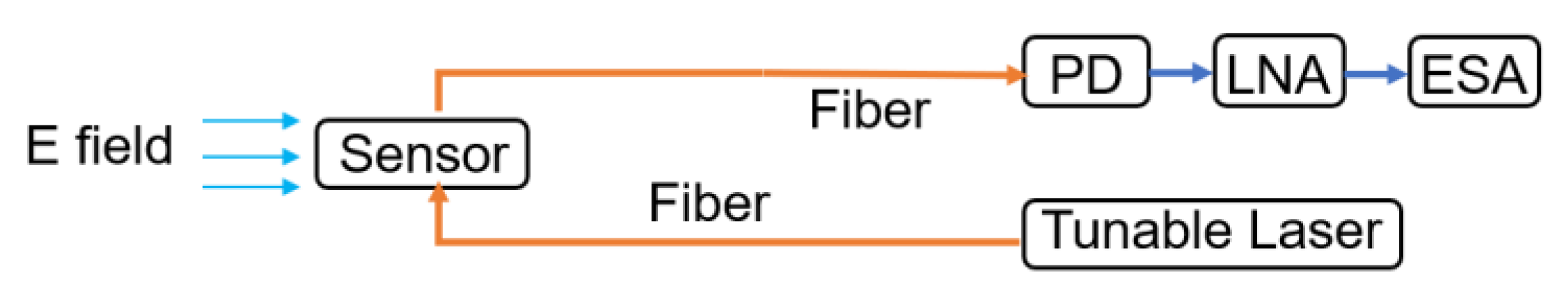
Figure 1 shows the proposed electric field sensing system. The sensor chip is exposed to the electric field and connected with a tunable laser and a photodetector (PD, Finisar, XPDV2120R) via optical fibers. The tunable laser is used to generate the optical carrier with a certain wavelength, which guarantees that the electric field sensor chip is biased at the linear transmission point. The electric signal is loaded onto the optical carrier via the sensor chip, and then demodulated by the PD. A low-noise amplifier (LNA, Qotana, DBLNA300011800A) after the PD is used to amplify the power of the received electric field. An electrical spectrum analyzer (ESA) is employed to measure the output signal power of the sensing system. Since the optical fiber is with an ultra-low transmission loss, the electric field sensor chip can be placed far away from other devices by using long fibers to realize remote sensing.
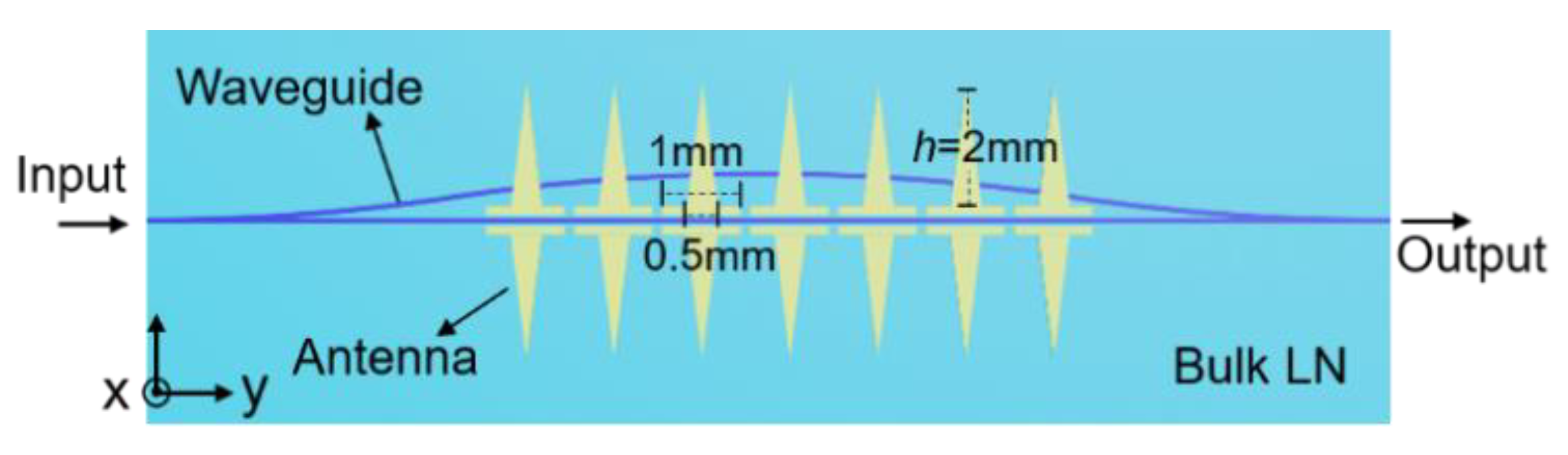
Figure 2 shows the schematic diagram of the sensor chip, which is fabricated on the x-cut y-propagating LiNbO
3 platform. The optical waveguide on the sensor chip possesses an AMZI architecture. There are seven pairs of tapered dipole antennas, arrayed along the straight waveguide in the lower arm of the AMZI, which are used to receive the external electromagnetic field. A voltage is generated by the received electric field between each pair of the tapered dipole antennas, which modulates the phase of the light wave in the lower arm via the Pockels effect. The phase modulation is converted to the intensity modulation via the AMZI, and thus the electric field can be demodulated in the PD. In the AMZI, an intrinsic phase difference of Δ
φ = 2
πneffΔ
L/λ is introduced between the light waves in the two arms, where Δ
L,
neff and
λ are the length difference between the two arms, the effective refractive index of the waveguide and the center wavelength of the light wave, respectively. Therefore, the transmission point of the sensor chip can be controlled through adjusting the output wavelength of the tunable laser instead of using an extra DC voltage source, which facilitates remote sensing without an electric power supply.
As shown in
Figure 2, the tapered dipole antennas are arrayed along the straight arm of the AMZI, and the modulation electrodes are at the bottom of the tapered dipole antennas. The flat frequency response of the tapered dipole antennas has been experimentally demonstrated [
11,
17]. The internal impedance per unit length corresponding to the axial coordinate
z can be expressed as [
18,
19]:
where
h is the length of a tapered antenna, as shown in
Figure 2.
Ψ is given by:
where
k is the wave number.
a is the equivalent radius of the dipole antenna.
C(x,y) and
S(x,y) are the generalized cosine and sine integrals, respectively. Then, the current distribution along the dipole antennas is given by:
where
V0 is the driven voltage. It can be seen from Equation (3) that the current distribution
I(
z) is unrelated to the frequency of the
V0, which indicates that the frequency response of the antenna is constant in a large frequency range.
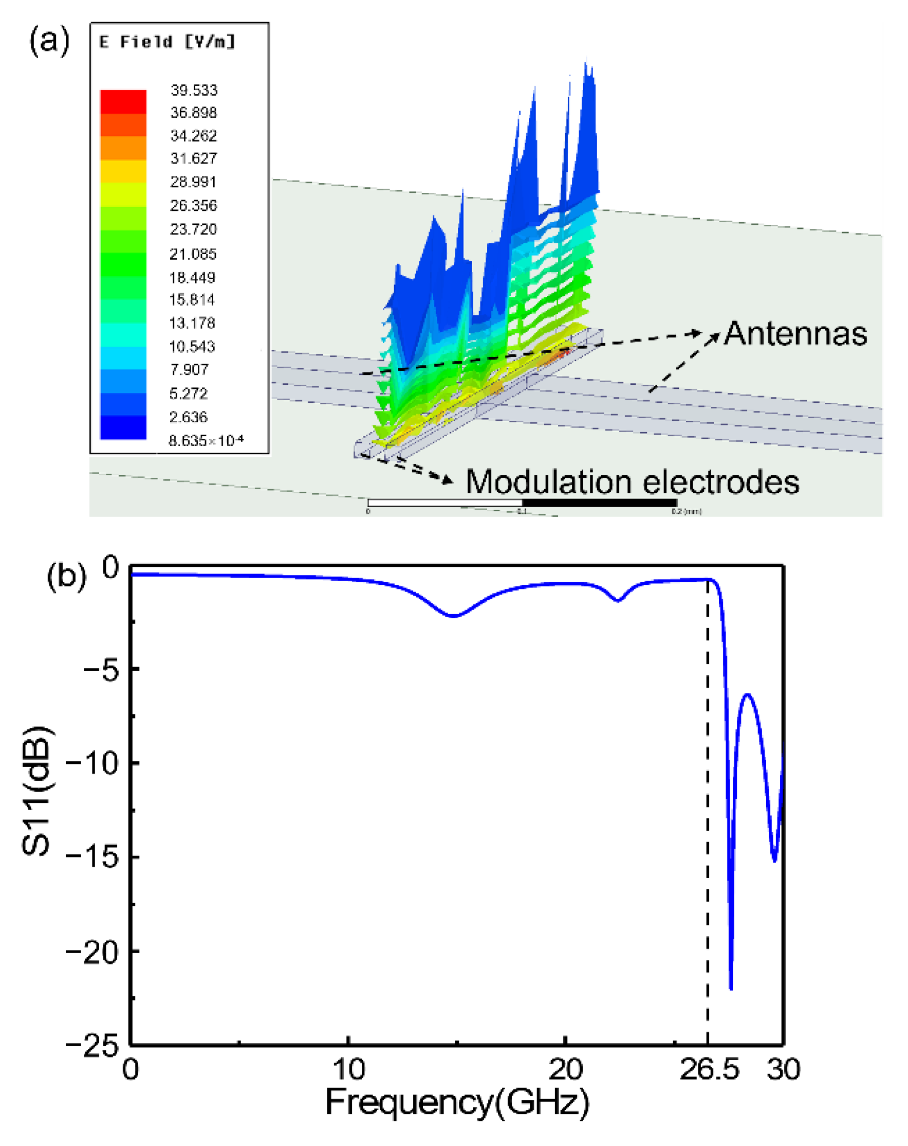
Simulation is implemented by using a high-frequency structure simulator (HFSS) to investigate the electric field distribution and the frequency response of a pair of tapered dipole antennas. In the simulation, every modulation electrode has a length of 2 mm and a width of 10 μm. The bottom width of the tapered antenna is 1 mm, and the height
h is 2 mm. The polarization direction of the induced voltage is perpendicular to the waveguide. The electric field distribution between the modulation electrodes is depicted in
Figure 3a, where the external electric field excitation is 1 V/m. It can be seen from
Figure 3a that the maximum electric field between the modulation electrodes is 39.5 V/m, which has an electromagnetic enhancement of nearly 40 times. Besides, the power reflection S11 is depicted in
Figure 3b. The S11 up to 26.5 GHz is relatively flat, which indicates that the response of the antenna is weakly dependent on the operation frequency. Hence, the measurement results are more convincing and predictable in the frequency range even without calibrating the amplitude with a standard electric field.
3. Measurements and Results
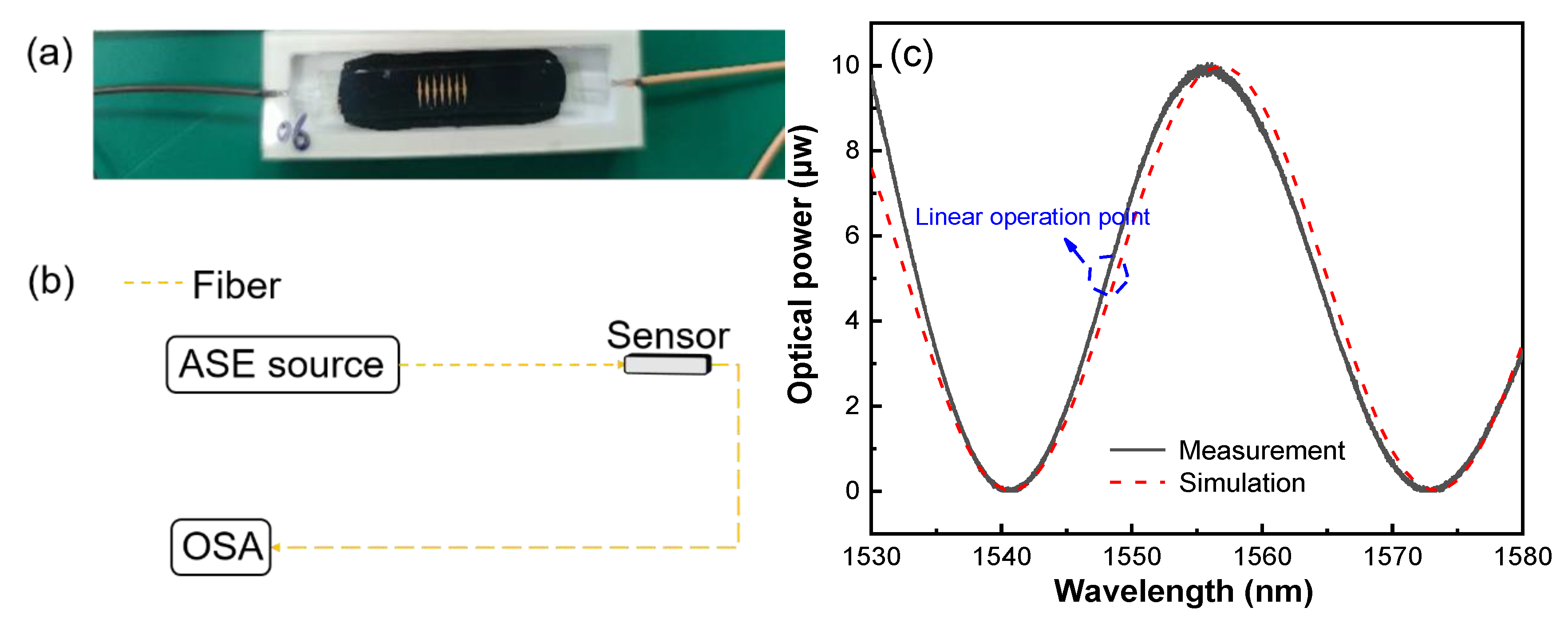
The fabricated sensor chip is displayed in
Figure 4a, where the parameters of the tapered dipole antennas are consistent with the simulation parameters given above. The Δ
L of the AMZI is designed to be about 34 μm, which corresponds to a free spectral range of about 30 nm. The output optical spectrum from the sensor chip is measured by employing an amplified spontaneous emission optical source (Glight OS321498) and an optical spectrum analyzer (Yokogawa AQ6370D), as shown in
Figure 4b. The measurement result agrees well with the calculation curve, as shown in
Figure 4c. The center wavelength of the tunable laser (Santec TSL-510) can be tuned from 1530 nm to 1560 nm to guarantee the suitable transmission point. The linear transmission point is at the half of the maximum output optical power, as depicted in
Figure 4c, and thus can be adjusted optically without a DC power supply, which has the implementation potential in the power supply-free remote sensing. In the following experiments, the wavelength of the tunable laser is set to be 1547 nm. In this condition, the sensor chip works at the linear operation mode.
A standard electric field is generated to accurately measure and calibrate the response of the sensor chip. The frequency response of the electric field sensor chip is measured from 10 MHz to 26.5 GHz.
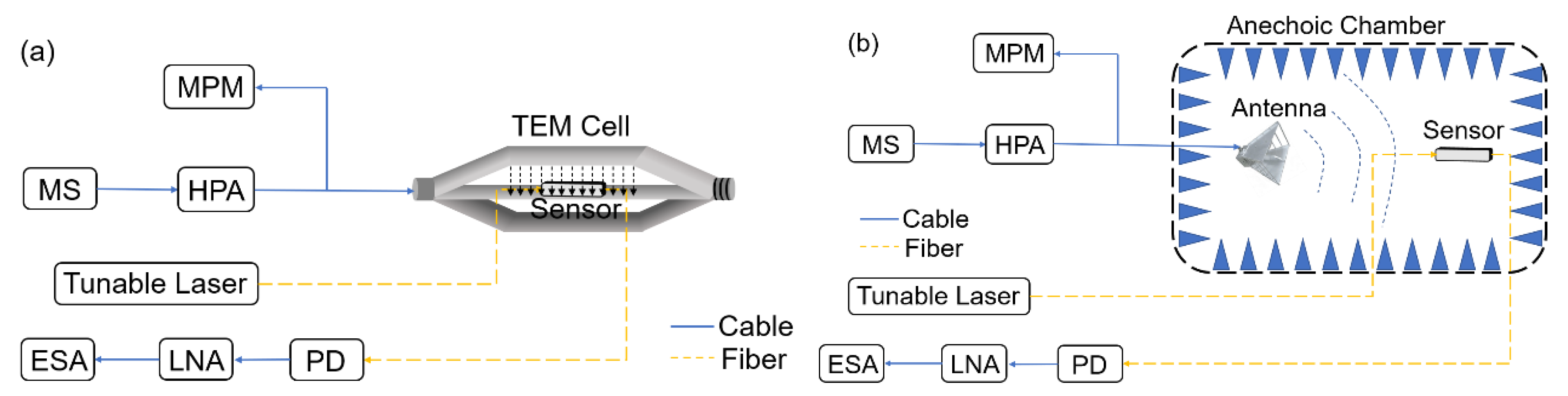
Figure 5a shows the measurement system based on a TEM cell, which is inherently a rectangular waveguide transmission line (open-ended waveguide). The TEM cell can generate a uniform electrical field whose polarization is perpendicular to the parallel metal plates. The generated electric field is strongly constrained between the metal plates, which avoids the measurement uncertainty induced by the interference via space coupling from the TEM cell to the ESA. The amplitude of the electric field is set to be 40 V/m by adjusting the output power of the microwave source (MS, Rohde & Schwarz SMCV 100B) and the high-power amplifier (HPA). The electrical power injected into the TEM cell (parallel metal plates with distance of 3 cm) is 14.6 dBm, which corresponds to a voltage of 1.2 V. To ensure the accuracy of the frequency response measurement, the amplitude uncertainty is maintained at a level smaller than ±1 dB by monitoring the input power of the TEM cell via a microwave power meter (MPM). The sensor chip is placed in the TEM cell, where the propagation direction of the optical wave is identical to that of the EM wave. Meanwhile, the polarization of the dipole tapered antennas is parallel to the polarization direction of the electric field. The TEM cell is applied to achieve frequency response measurement from 0.1 GHz to 1 GHz. In order to achieve higher frequency response measurement, a standard electric field is generated by a series of standard gain horn antennas, as shown in
Figure 5b. The amplitude of the electric field is calibrated to be 40 V/m by adjusting the relative position of the sensor chip. Different from the measurement environment of the TEM cell, the standard gain horn antennas and the electric field sensor chip are placed in the anechoic chamber to shield the original electric field radiation. A few discrete frequency points, i.e., 4.8 GHz, 10 GHz, 14 GHz, 18 GHz, and 26.5 GHz, are calibrated to be with an amplitude of 40 V/m, which are used as the standard electric field to measure the response of the sensor chip. In the experiment, the signal power is measured by using an ESA (Rohde & Schwarz FSV3007).
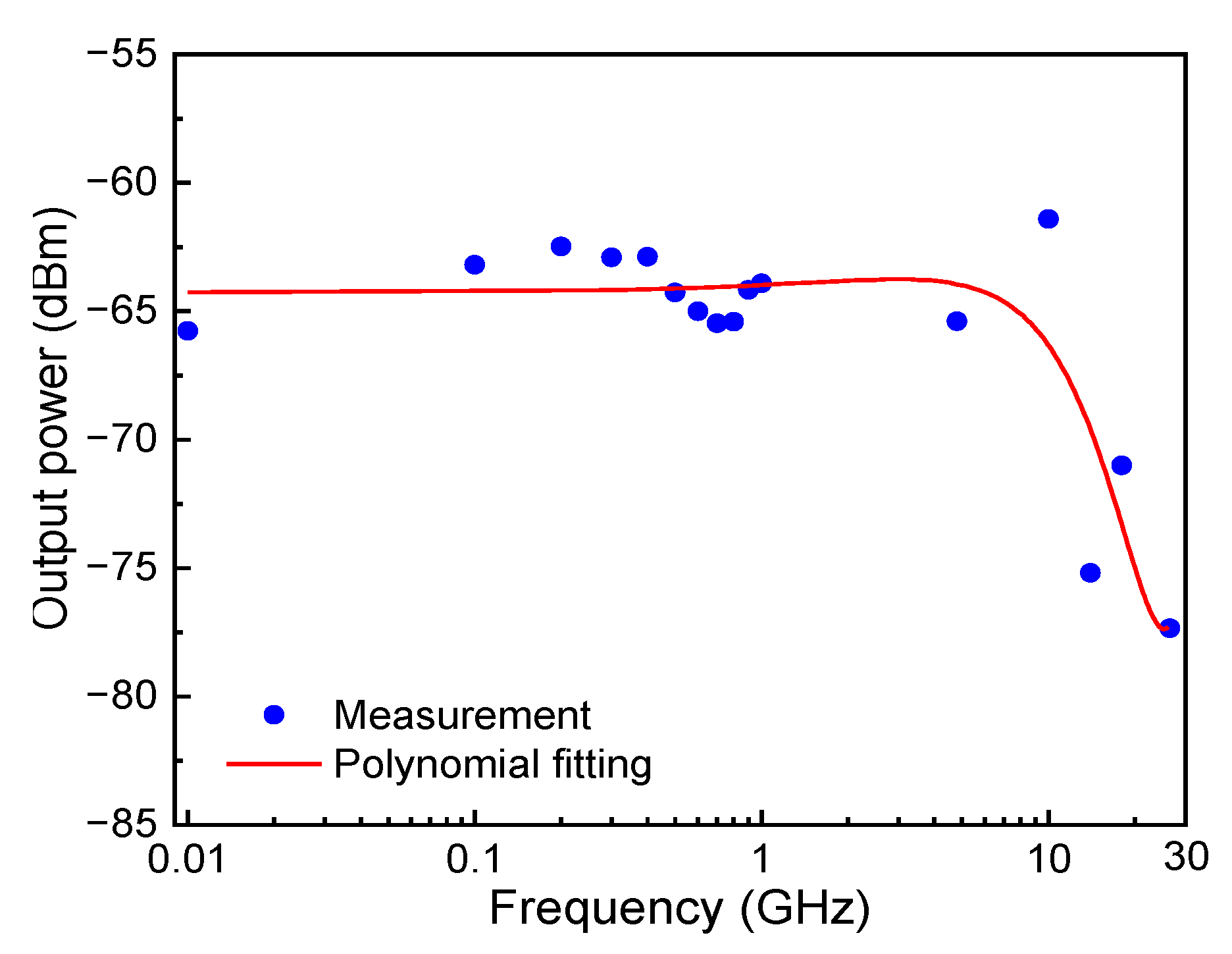
Figure 6 shows the measured frequency response of the sensor chip in the standard electric field. In the measurement, the resolution bandwidth (RBW) of the ESA is set to 1 kHz. On this condition, the noise floor is measured to be −105 dBm. It can be seen from
Figure 6 that the signal–noise ratio (SNR) is larger than 40 dB in the frequency range of 10 MHz to 26.5 GHz, indicating that the electric field sensor chip has an operation bandwidth over 26.5 GHz. The sensitivity of the sensor chip is calculated to be 12.36 mV/m/Hz
1/2, which is a little poorer than that in Ref. [
16]. This is attributed to the short electro-optical interaction length in our sensor chip. However, the operation bandwidth of our sensor chip is much larger than that of the device in Ref. [
16]. The degradation of the frequency response over 10 GHz is attributed to the velocity mismatch of the optical wave and the electromagnetic wave in the travelling wave modulation, where the effective refractive indices of the electromagnetic wave in the free space and the optical wave in the LN waveguide are equal to 1 and 2.14, respectively. This velocity mismatch results in a serious decline of the modulation efficiency in travelling wave modulation when the sensor chip is used to detect high-frequency electromagnetic waves.
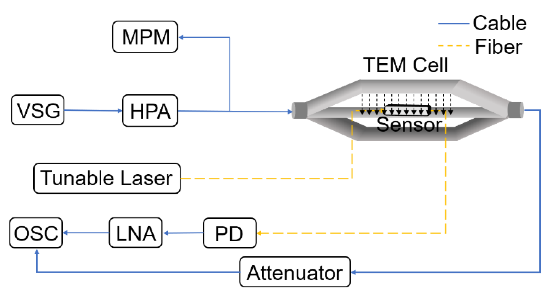
The sensing ability of OOK signals is investigated using the sensor chip. The sensing system is shown in
Figure 7, where OOK signals from the vector signal generator (VSG) and the sensing system are recorded by employing a high-speed real-time oscilloscope (Tektronix DPO75002SX). In the experiment, the power of the OOK signal is set to be 25 dBm, i.e., the amplitude of the electric field is 133 V/m. The employed OOK signals are set to have a center frequency of 3 GHz and bit rates from 1 Mb/s to 40 Mb/s, respectively. To protect the oscilloscope from being damaged by a high voltage, a power attenuation of 30 dB is applied to the OOK signal from the vector signal generator when the signal from the VSG is directly sent to the oscilloscope.
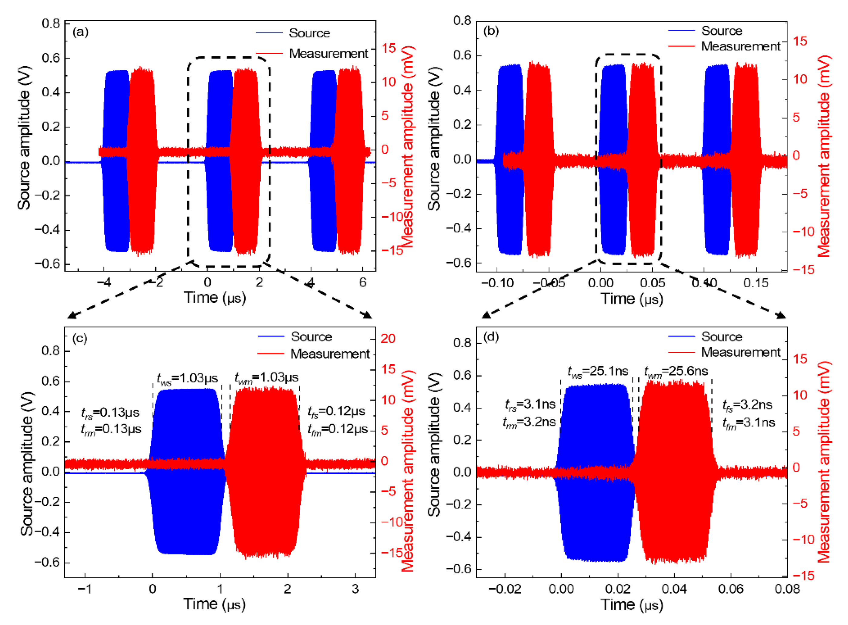
The recorded OOK signals are shown in
Figure 8, which are averaged 500 times to compress the random noise and to increase the SNR. In order to evaluate the signal distortion, the rise time
tr, the fall time
tf and the pulse width
tw of the signal envelope are measured, where
tr is defined as the time from 10% to 90% of the maximum amplitude,
tf is defined as the time from 90% to 10% of the maximum amplitude, and
tw is defined as the time from the rise edge to the fall edge at the point of 50% of the maximum amplitude. The measured
tr,
tf and
tw of the OOK signals from the sensing system and the VSG (the subscript
m and
s, respectively) are depicted in
Figure 8c,d.
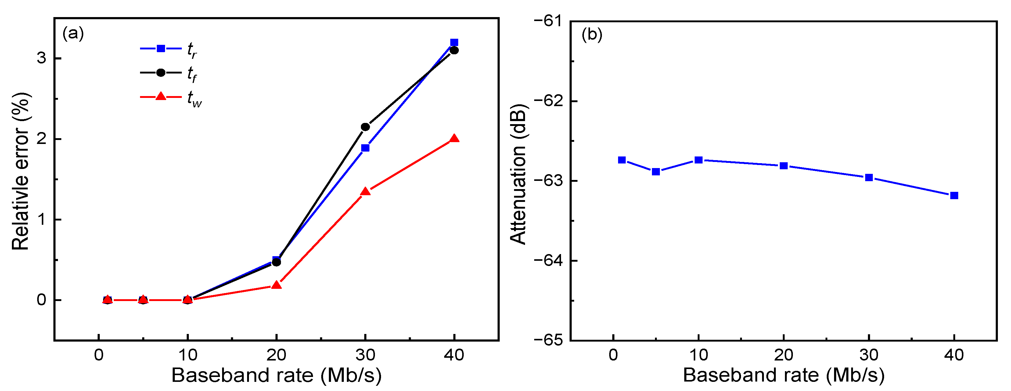
The relative measurement errors of
tr,
tf and
tw under different bit rates are shown in
Figure 9a, which indicates that the relative measurement errors of
tr,
tf and
tw increase as the bit rate increases. However, the relative measurement error is smaller than 3.5% even under a bit rate of 40 Mb/s.
Figure 9b shows the signal power attenuation after the sensing system under different bit rates, where the power variation is smaller than 0.5 dB.
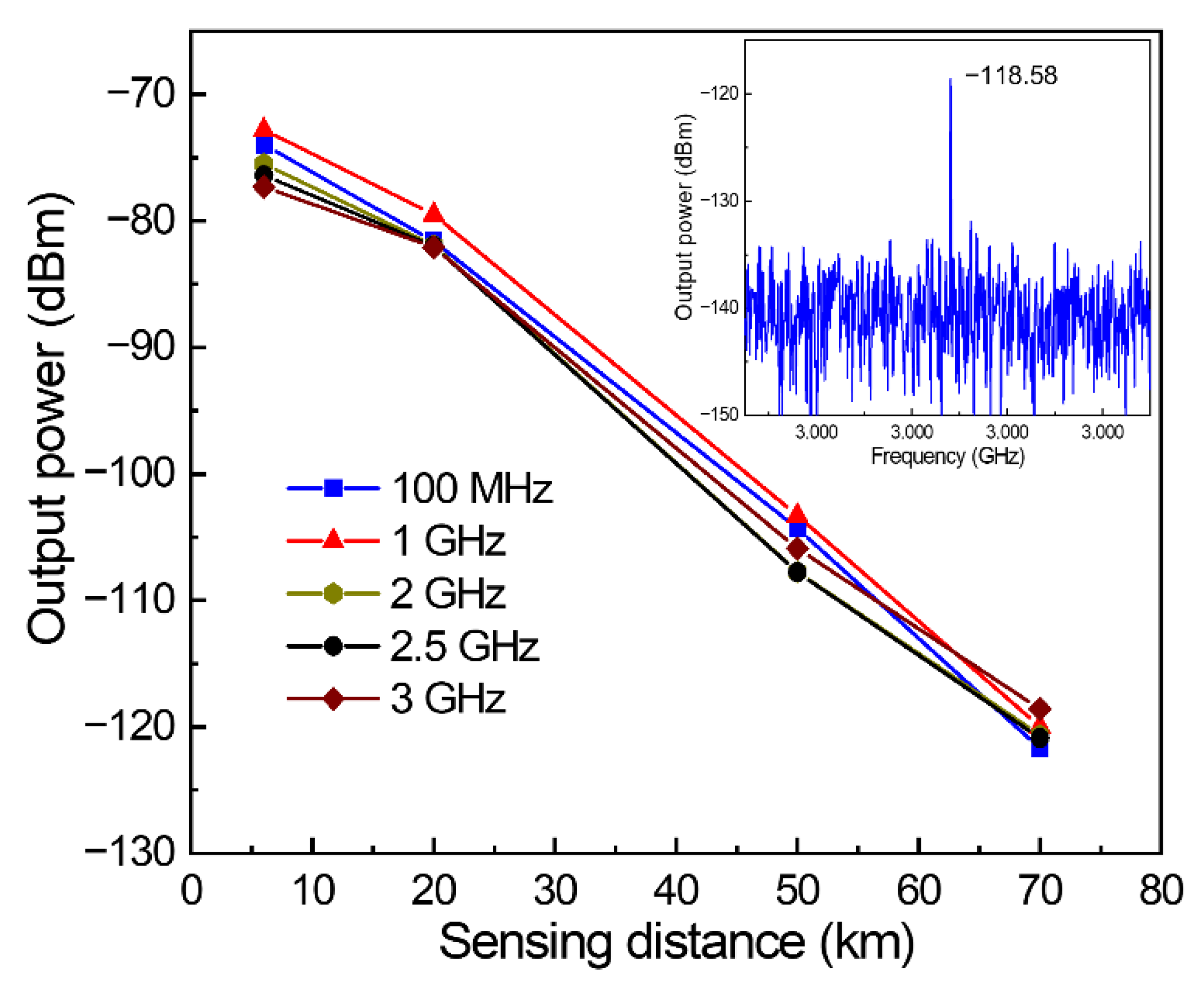
Remote sensing is also demonstrated based on the system shown in
Figure 5a. In the experiment, the sensor chip is placed in the TEM cell. Single-tone microwave signals at 100 MHz, 1 GHz, 2 GHz, 2.5 GHz, and 3 GHz and with an identical amplitude of 40 V/m are generated in the TEM cell. Two spools of single-mode fiber are employed to connect the laser, the sensor chip and the PD. In order to guarantee that the measured signal comes from the sensor chip instead of the free space radiation from the TEM cell to the ESA, the TEM cell and the ESA are placed in two rooms, respectively. On this condition, the radiated signal power from the TEM cell to the ESA through free space is measured to be lower than the noise floor of the ESA, with a RBW of 1 Hz. Remote sensing is demonstrated, with distances of 6 km, 20 km, 50 km and 70 km. In the measurement, the RBW of the ESA is set to be 1 Hz, where the noise floor is measured to be −140 dBm.
Figure 10 shows the measured signal power under different sensing distances. The signal power decreases as the sensing distance increases, as depicted in
Figure 10. However, the SNR of the 70 km remote sensing at 3 GHz is still over 20 dB. In the remote sensing experiment, different spools of optical fiber are used to emulate different sensing distance.
Table 1 lists the measured loss of the optical fibers used in the experiment. These fibers do not have an identical loss coefficient, i.e., 0.33 dB/km and 0.3 dB/km for the input and output of a 6 km-long fiber, 0.25 dB/km and 0.24 dB/km for the input and output of a 20 km-long fiber, 0.218 dB/km and 0.216 dB/km for the input and output of a 50 km-long fiber, and 0.23 dB/km and 0.225 dB/km for the input and output of a 70 km-long fiber. The degradation of the signal power with the increasing distance in
Figure 10 is consistent with the optical loss of the fibers. Benefiting from the low insertion loss of the optical fiber, long-distance remote sensing, based on the proposed photonic electric field sensor chip, is feasible.

 ,
, 


