Nano-Bismuth-Sulfide for Advanced Optoelectronics

1
Department of Network and New Media, Hunan City University, Yiyang 413000, China
2
School of Information and Electronic Engineering, Hunan City University, Yiyang 413000, China
3
Xi’an Micro Microelectronics Technology Institute, CASC, Xi’an 710054, China
*
Author to whom correspondence should be addressed.
Photonics 2022, 9(11), 790; https://doi.org/10.3390/photonics9110790
Submission received: 31 August 2022
/
Revised: 9 October 2022
/
Accepted: 18 October 2022
/
Published: 24 October 2022
(This article belongs to the Topic Optical and Optoelectronic Materials and Applications)
Abstract
:Bi2S3is a semiconductor with rational band gap around near-IR and visible range, and its nanostructures (or nano-Bi2S3) have attracted great attention due to its promising performances in optoelectronic materials and devices. An increasing number of reports point to the potential of such nanostructures to support a number of optical applications, such as photodetectors, solar cells and photocatalysts. With the aim of providing a comprehensive basis for exploiting the full potential of Bi2S3 nanostructures on optoelectronics, we review the current progress in their controlled fabrication, the trends reported (from theoretical calculations and experimental observations) in their electrical properties and optical response, and their emerging applications.
1. Introduction
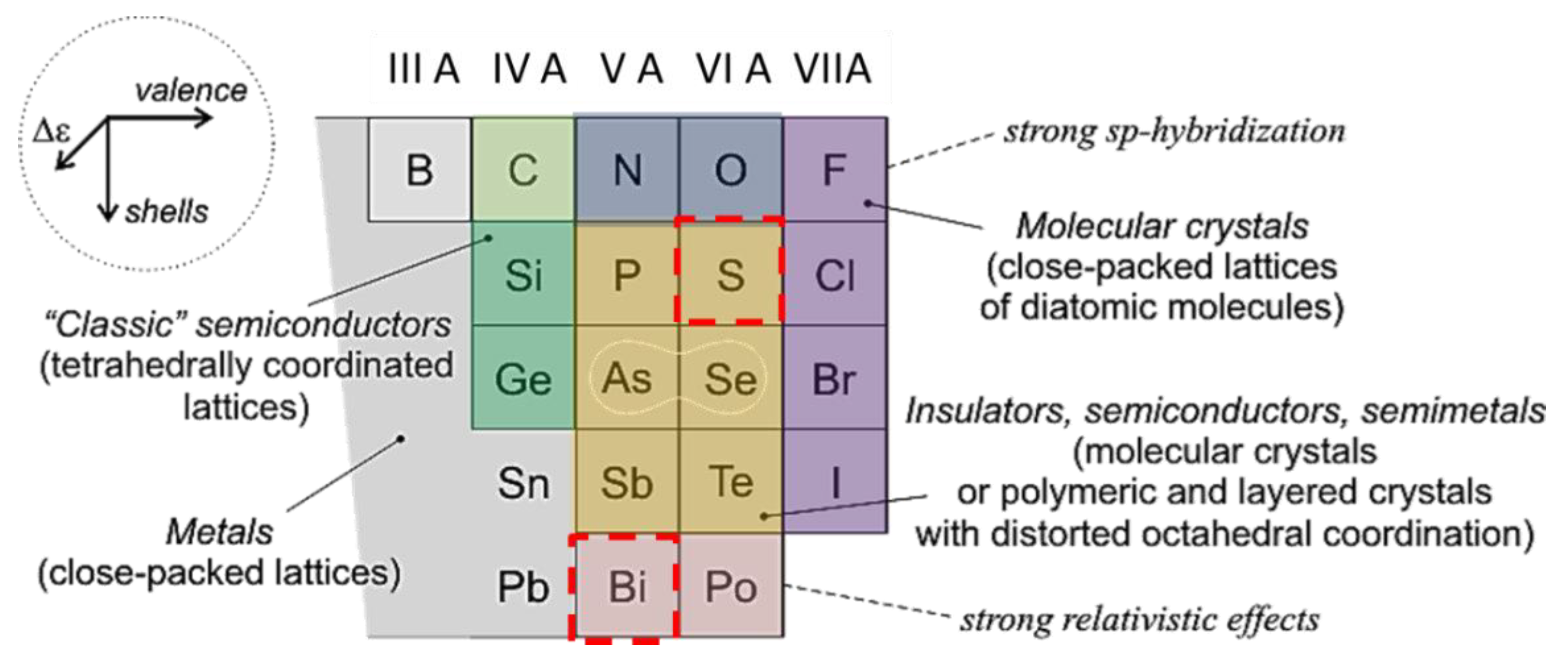
Chalcogenide materials are chemical compounds consisting of at least one chalcogen ion, i.e., a chemical element in column VI of the periodic table, also known as the oxygen family [1]. More precisely, the term chalcogenide refers to the sulphides (S), selenides (Se), and tellurides (Te). These compounds show similar patterns in their electron configuration (Figure 1), especially the outermost shells, resulting in similar trends in chemical behavior. On one hand, they are different from IV family elements such as silicon (Si) and germanium (Ge), serving as the “classic” semiconductors with tetrahedral coordinated lattices due to their strong covalent bonding. On the other hand, unlike the elements of the halogen family, with strong sp-hybridization for forming crystalline molecular structures, chalcogenide elements could form rich materials, including insulators, semiconductors as well as semimetals. These materials could be either molecular crystals or polymeric and layered crystals with distorted octahedral coordination. Such rich chemical and lattice structural features produce abundant electrical and optical properties. Accordingly, over the last decade, chalcogenide materials have attracted much attention, and intensive studies demonstrate their promising applications in phase change memory (PCM) [2], topological insulators [3], photo-catalysts [4], light-sources [5], etc.
Besides the unique properties of chalcogenide elements themselves, the chemical and physical behaviors of the chalcogenide materials also strongly depend on the elements to be chemically combined. Bismuth (Bi), as an outstanding p-block semimetal with a highly anisotropic Fermi surface [6], small effective electron mass, low carrier density, and long carrier mean-free path, can produce a strong relativistic effect [7]. Therefore the bismuth chalcogenide compounds, such as Bi2Se3, Bi2Te3 and Bi2S3, have a number of notable chemical and physical properties [1,3,7], and have attained increasing significance for several fields, including quantum confinement [8], topological insulators [3], abnormal magnetoresistance [9], energy storage and conversion [10,11], thermoelectricity [12], etc. Hence, it is of value to review the current status of bismuth chalcogenide materials. In recent years, however, more attention has been paid to Bi2Se3 and Bi2Te3, which are “star” materials, being well-known topological insulators [3], whereas the awareness of the advances on Bi2S3 materials is relatively sparse. However, as a n-type semiconductor with relative low symmetric space group [13], Bi2S3 shows great potential in solar cells [14], hydrogen storage [15], photo-catalysts [16], optical-detection [17], memristors [18,19], etc. Moreover, in these applications, constructing nanostructures with rich surface sites seems of great significance, thanks to their strong nano-size effect [13,18,20,21,22]. Therefore, it is valuable to review the research progress on nano-bismuth-sulfide. In this paper, we review recent advances in bismuth-sulfide nanostructures for optoelectronics to track the rapid development in this field, highlight the most recent scientific discoveries, and predict future trends for nano-bismuth-sulfide as well as its applications.
The remainder of this paper is organized as follows: Section 2 discusses various fabrication methods of nano-Bi2S3; Section 3 describes the basic electronic and optical properties of Bi2S3; Section 4 focuses on the emerging optoelectronic applications. Finally, conclusions and perspectives are drawn in Section 5.
2. Fabrications
Amount of Bi2S3 nanostructures were successfully prepared, namely 0D nanostructures (e.g., nanoparticles and nanospheres), 1D nanostructures (including nanowires and nanorods), and 2D nanostructures (including nanoplates, nanosheets, and thin films), with continuously improved crystalline quality [13,16,17,18,23,24,25,26,27,28,29,30,31,32,33,34,35,36,37,38,39,40,41,42,43,44,45,46,47]. The sizes of these structures range from a few atoms to a few microns, which makes them broadly suitable for studies in various fields, including hydrogen storage [48], thermoelectricity [46], memristors [21], photocatalysts [49], solar cells [26], and photodetection [50]. It is doubtless that the broad size range of the existing Bi2S3 nanostructures could provide abundant building blocks for constructing optical responsible systems.
Actually, over the past few years, the fabrication methods of Bi2S3 nanostructures were explored intensively (see Table 1). Physical or chemical deposition and direct solvothermal synthesis are commonly employed, while some other methods, including chemical precipitation, reflux, sol-gel method, hot-injection, and high power sonication process have also been reported [4,16,32,51,52]. These methods can produce 0D nanoparticles, 1D nanorods, and nanoribbon, as well as 2D nano-thin film. The solution-phase synthesis is the most frequently employed method utilized to prepare various Bi2S3 nanostructures [23,27,28] while physical vapor depositions (PVD, including magnetron sputter thermal evaporation and pulse laser deposition) have demonstrated their value in the photovoltaic field for electron-transport layers (ETL) and light-absorption layers [14,26]. Especially for hybrid perovskite solar cells, when potential contamination and variations introduced by the solvents are undesired, thermal evaporation is proposed as a rational route for preparing Bi2S3 nano-thin film as the ETL without introducing any solvents [26]. Generally, the fabrication methods of the nano-Bi2S3 can be cataloged as two types: “top-down” and “bottom up”. It is quite straightforward that several vapor or liquid phase-deposition methods belong to the “top-down” family, and direct surface sulfurization is also an alternative “top-down” approach, while solvothermal synthesis is the most popular “bottom up” method. In the following, these two kinds of methods are discussed sequentially.
Vapor phase deposition (VPD) is one of most frequently used methods for nanofabrication, with the potential for mass production [7]. It has achieved great successes in various field, including integrated circuits [53], semiconductor lasers [54], bio-sensing [55], etc. For the preparation of nano-Bi2S3, especially thin film, VPD, such as thermal evaporation (Figure 2a), pulse laser deposition (PLD), and low-pressure metal–organic chemical vapor deposition (LP-MOCVD) could be feasible tools [14,26,56]. Moreover, while regularly employed in light-absorption layers [56], VPD-fabricated nano-Bi2S3 also exhibits unique value as high performance inorganic electron transport layers for perovskite solar cells to avoid contamination and variations introduced by the solvent process [26], as well as serving as energy conversion media for quantum dot-sensitized solar cells (QDSSCs) [14]. In addition to the VPD methods, Bi2S3 thin film can also be prepared by chemical bath or electrochemical deposition [33,57]. These deposition routes may introduce impurity or contamination, but could be more cost-effective (Figure 2b). Moreover, using a vapor-phase sulfur source to sulfurize the bismuth-based metal-organic framework or bismuth oxide could achieve “top-down” Bi2S3 nanostructures (Figure 2c–e) [29]. These surface sulfurization routes need high temperature, but could provide better crystalline quality.
Aside from the “top-down” deposition, “bottom-up” solvothermal synthesis seems more popular for the fabrication of various Bi2S3 samples with a high level of control in their shapes, such as 0D, 1D, and 2D nanostructures [17,28,30,34,58,59]. As the liquid-phase progresses, it employs the bismuth source and sulfur source to react in solution. Bi(NO3)3 is the most popular bismuth source, but some other choices, such as BiCl3 and BiOX (X = Cl, Br, I) are also available [11,33,60,61], while the sulfur source could be either organic (TAA, KSCN, etc.) or inorganic (Na2S, Na2S2O3). The reaction temperatures are usually moderate (<200 °C), and the synthesis duration varies from a few minutes to a few days [39,58]. The most typical product of the solvothermal synthesis is the 1D rod or wire (Figure 2f). The diameter of the nanorod or nanowire is <100 nm, while the length could be facile to tens μm. Such 1D growth often tends to extend along the [001] direction, with a corresponding length-to-diameter ratio greater than 10 [22]. When the hydrothermal synthesis is assisted with glucose, hollow nanotubes can also be produced by 1D growth [60]. In addition, nanoribbon can also be solvothermally synthesized, and interestingly, the process is rather fast (a few minutes), possibly representing an highly efficient route to mass production [58]. Moreover, in some other cases, due to the change in the sulfur source, the morphology could transform from nanowire to nanoparticles, wire bundles, urchin-like nano-/microspheres, or microspheres with cavities, as well as chrysanthemum-like Bi2S3 nanostructures [59].

Table 1.
Selected reports on “top-down” and “bottom-up” fabrication of the nano-Bi2S3.
| Method | Growth Condition | Starting Materials | Product | Size |
|---|---|---|---|---|
| “Top-down” fabrications | ||||
| Vapor phase deposition | ||||
| Thermal evaporation [26] | RT | Bi2S3 power | Amorphous film | 50 nm thickness |
| LP-MOCVD [56] | 450 °C | [Bi(S2CNMen-Hex)3] [Cd(S2CNMen-Hex)2] | Fiber-like particles | Length (L): 1 μm diameter (D): 50 nm |
| Pulsed laser deposition [14] | RT | Bi2S3 target | Quantum dots | D < 5 nm |
| Liquid phase deposition | ||||
| Cathodic electrodeposition [41] | RT | Na2S2O3, Na3C6H5O7Bi(NO3)3, | Thin film | / |
| Electrodeposition [62] | RT | Na2S2O3, Bi(NO3)3, EDTA | Thin film | / |
| Chemical bath deposition(CBD) [33] | RT | Bi(NO3)3, thioacetamide (TA), ammonium citrate (AC) | Nanowall Bi2S3 films | / |
| CBD [26] | RT | Bi(NO3)3,triethanolamie (TEA), TA, | Thin film | Thickness (T): 50–140 nm |
| Non-aqueous CBD [63] | RT | Bi(NO3)3,acetic acid, TA | Thin films | T: 241 nm |
| Non-aqueous CBD [42] | RT | Bi(NO3)3, Na2S2O3, formaldehyde, | Thin film | T: 50–100 nm |
| Surface Sulfurization | ||||
| High-temperature reaction of sulfur source with bismuth-based metal–organic framework [64] | 300~600 °C | Bi(BTC)(DMF)·DMF·(CH3OH)2 Trimesic acid (H3BTC) | Nanorod (NR) | D: 60 nm |
| Surface sulfurization [29] | 450 °C | Bi2O3 Nanosheets | 2D nanosheets | T: 2.5 nm |
| “Bottom-up” fabrications | ||||
| Solvothermal synthesis | ||||
| Hydrothermal synthesis [30] | 160 °C | Bi(NO3)3, NH2CSNH2, thiourea | NR | D: 50~100 nm L: 1~2 μm |
| Hydrothermal process [11] | 180 °C | BiCl3, HCl, TAA | Bi2S3 nanomeshes | L: 200 nm D: 20~40 nm |
| Hydrothermal process [65] | 180 °C | Bi(NO3)3, Thiourea, Urea, Methyl orange | Microsphere | D: 3 μm |
| Hydrothermal methods [59] | 180 °C | Bi(NO3)3, thiourea (TU), potassium thiocyanate (KSCN), TAA, sodium thiosulfate (Na2S2O3·5H2O) | Nanowires (NW), wire bundles, urchin-like nano-/microspheres microspheres with cavities | NW D:15~40 nm L: Tens μm bundles D: 2~3 μm L: 13~20 μm sphere D: ~1 μm/ |
| Solvothermal synthesis [66] | 160 °C | Bi(NO3)3, ethylene glycol (EG), TAA, TU, L-cysteine | Nanoparticles, urchin-like spheres | / |
| solvothermal method [67] | 80 °C | Bi(NO3)3, EG, TU, poly(vinylpyrrolidone) (K-30) | Chrysanthemum- like nano-Bi2S3 | D: ~500 nm. |
| Solvothermal method [58] | 150 °C 5 min | Oleyl amine, sulfur powder, BiCl3, oleic acid, hexane, 1-octadecene | Nanoribbons | D:10~80 nm L:100~500 nm |
| Hydrothermal route [68] | 160 °C | Bi(NO3)3, TAA, DA, ascorbic acid (AA), uric acid (UA), paracetamol | NR | L:100 nm |
| Hydrothermal method [60] | 180 °C | Bi(NO3)3, Na2S2O3, glucose | Hollow nanotubes | L: dozens μm D: few μm |
| Hydrothermal method [43] | 180 °C 2 days | Bi(NO3)3, Na2S2O3, | NW | D: 20–60 nm |
| Hydrothermal method [39] | 180 °C 3 day | Tetramethylammonium Bi(NO3)3, hydroxide, Na2S | NW | D: 60 nm |
| Wet chemical synthesis [69] | 150 °C/1 h and then 240 °C/2 h | Bi(NO3)3,methanol, hydrochloric acid, thiourea | NR | D: 20–40 nm L: 200–600 nm |
| Other methods | ||||
| Chemical precipitation [32] | 70 °C | Bi(NO3)3,Thioacetamide (C2H5NS), HCl | Nanoparticle | D: 10~50 nm |
| Reflux [16] | 140 °C | Bi(NO3)3, citric acid, TU, CTAB DMF, EG, PEG | NR, nanoparticle | D < 40 nm |
| Sol-gel method [51,52] | 180 °C | Bi(NO3)3, TU, polyvinyl pyrrolidone, lithium hydroxide, EG | NR | D: 200 nm |
| Hot-injection [4] | 180 °C | Bismuth chloride thioacetamide | NR | D: 7~20 nm, L: 30~70 nm |
| High power sonication process [24] | RT | Bi2S3 powder | Nanoribbons | L: ~10 μm Width (W): ~40 nm |
Figure 2.
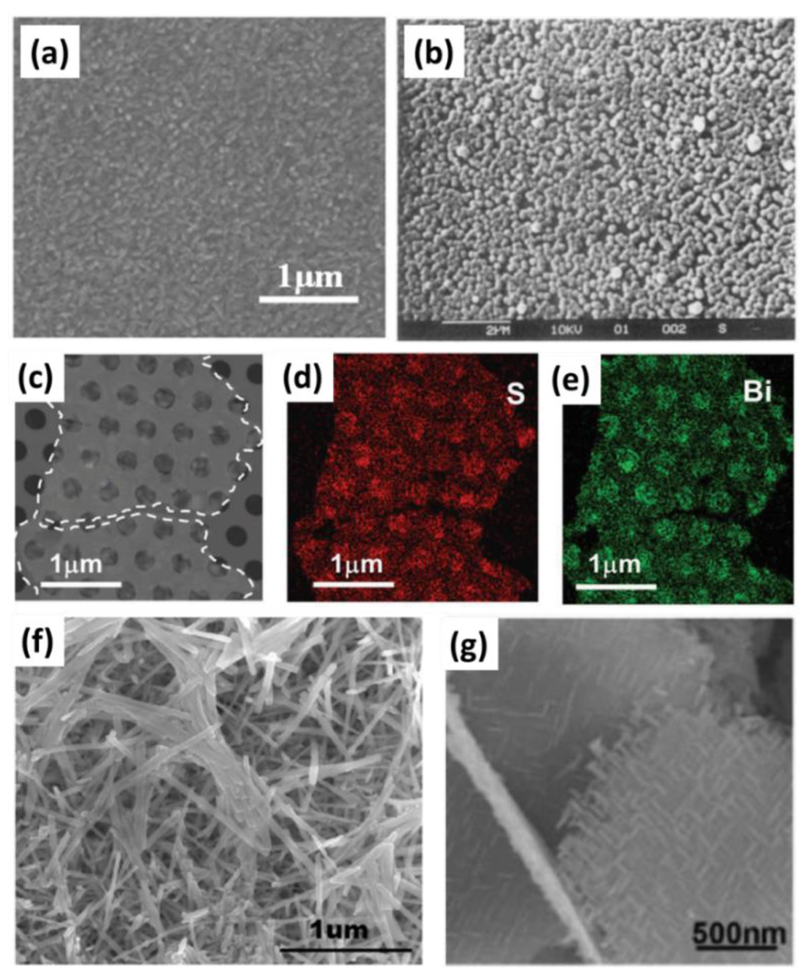
SEM of (a) Bi2S3 thin film prepared by thermal evaporation (reprinted with permission from [70] © 2022, Elsevier), (b) Bi2S3 thin film prepared by CBD (reprinted with permission from [42] © 2022, Elsevier). TEM image of (c) Bi2S3 nanosheet, as well as its (d) S-element and (e) Bi-element mapping (reprinted with permission from [29] © 2022, Wiley-VCH); SEM image of (f) Bi2S3 nanowire prepared by solvothermal synthesis (reprinted with permission from [43] © 2022, Elsevier) and (g) BiOCl–Bi2S3 hierarchical nanosheet (reprinted with permission from [28] © 2022, Wiley-VCH).
Figure 2.
SEM of (a) Bi2S3 thin film prepared by thermal evaporation (reprinted with permission from [70] © 2022, Elsevier), (b) Bi2S3 thin film prepared by CBD (reprinted with permission from [42] © 2022, Elsevier). TEM image of (c) Bi2S3 nanosheet, as well as its (d) S-element and (e) Bi-element mapping (reprinted with permission from [29] © 2022, Wiley-VCH); SEM image of (f) Bi2S3 nanowire prepared by solvothermal synthesis (reprinted with permission from [43] © 2022, Elsevier) and (g) BiOCl–Bi2S3 hierarchical nanosheet (reprinted with permission from [28] © 2022, Wiley-VCH).

Besides the pure Bi2S3 nanostructures, there are also several hierarchical and/or heterogeneous structures based on nano-Bi2S3 (Table 2), and they are fabricated (usually) through the combination of “top-down” and “bottom-up” routes [49,51,52,71,72,73,74] (Figure 2g). Thanks to the high surface-to-volume ratio of such nano-Bi2S3-based hierarchical and/or heterogeneous structures, they are quite promising for applications such as Li- or Na- ion battery, photocatalysts, and so on [10,52,73,75].
3. Optoelectronic Properties of Nano-Bismuth-Sulfide
3.1. Electronic Band Structure and Conduction Properties
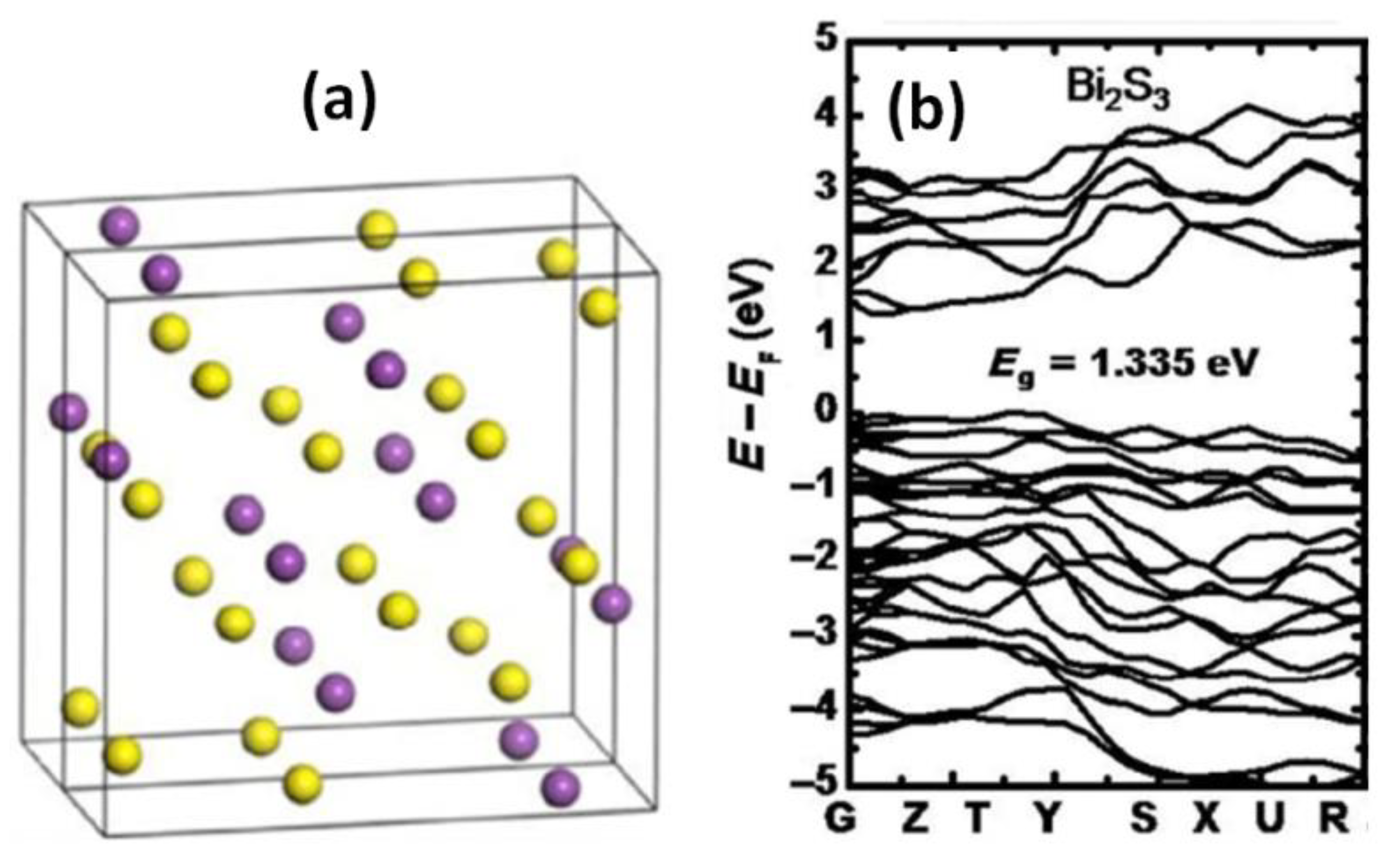
Bi2S3 has an orthorhombic crystal structure (a = 11.305 Å, b = 3.981 Å, c = 11.147 Å) with the space group pbnm (62) [13]. It has four molecules per unit cell [18,19], and each molecule contains two bismuth atoms and three sulfide atoms, which add up to 20 atoms per unit cell (Figure 3a). The relatively low symmetry of the space group implies that the crystal structure of Bi2S3 consists of five non-equivalent atoms: two non-equivalent Bi sites and three non-equivalent S sites [13]. It has a special layered structure and weak bonds between the layered units, which leads to the anisotropy of Bi2S3 growth [24]. Its band gap is 1.3~1.7 eV at room temperature (RT), and the first principle calculated value is 1.335 eV using a local density approach, as shown in Figure 3b [19]. However, if spin-orbit coupling (SOC) is considered, the band gap would decrease to ~1.2 eV [13]. These experimental and theoretical results indicate that Bi2S3 could produce a large absorption coefficient around the near-infrared and visual range [17,19,78]. Moreover, Bi2S3 is intrinsically n-type, with a carrier concentration of n = 3 × 1018 cm−3 at RT, and its RT electron mobility is μn = 200 cm2/Vs [26]. Accordingly, the intrinsic RT resistivity of Bi2S3 is ~105 Ω cm. Furthermore, the electrical conduction of Bi2S3 is temperature dependent due to its semiconduction nature, and highly anisotropic due to its low crystalline symmetry [79]. It can exhibit temperature-dependent conduction activation behavior, and potentially unique thermoelectric behavior, which could be used for thermal power devices [12,80]. It also has several other interesting electrical properties, including the Meyer–Neldel rule (MNR), resistive switching, etc. [18,19,81].
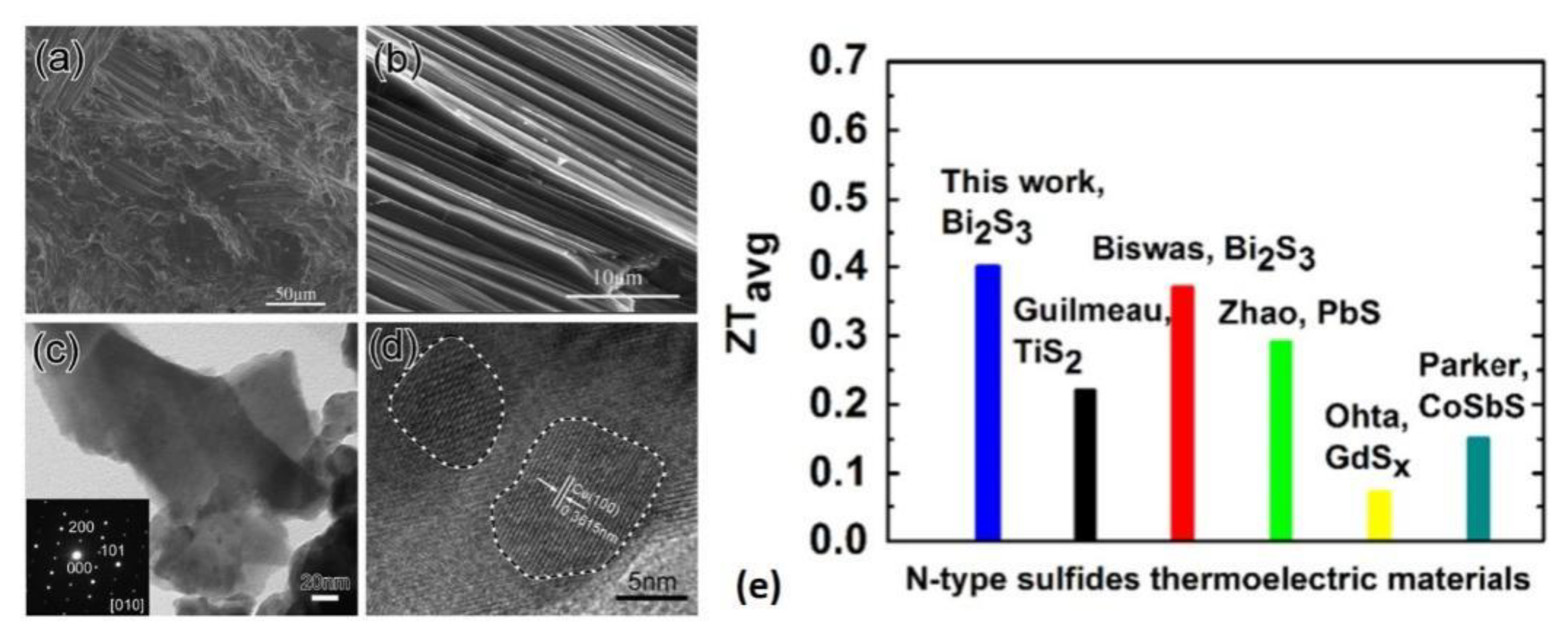
For the thermal power feature of Bi2S3, the typical Seebeck coefficient of Bi2S3 could be higher than 400 μV K−1, and its figure of merit (ZT value) could reach 0.72 at 773 K with rational CuBr2 doping (Figure 4a–d), and even the average ZT value over the temperature from 300 K to 773 K, for more accurate evaluation of the thermoelectric efficiency, is still up to 0.40 (see Figure 4e) [82]. These promising reports make Bi2S3, Bi2Se3, and Bi2Te3 a potential material family for heat-energy conversion [12,46,83]. Moreover, nano-structured bulk samples of Bi2S3 made from surface-treated Bi2S3 nanonetworks present ZT of 0.5 at 723 K [76], thanks to its improved electrical conductivity and low thermal conductivity compared with samples made from solution-synthesized materials or ball-milled powders. Moreover, as nano-scale Bi2S3 precipitates, it seems beneficial to improve the thermoelectric property of CuxBi2SeS2 [28]. Some selected reports about Bi2S3-based the thermal power device are listed in Table 3.
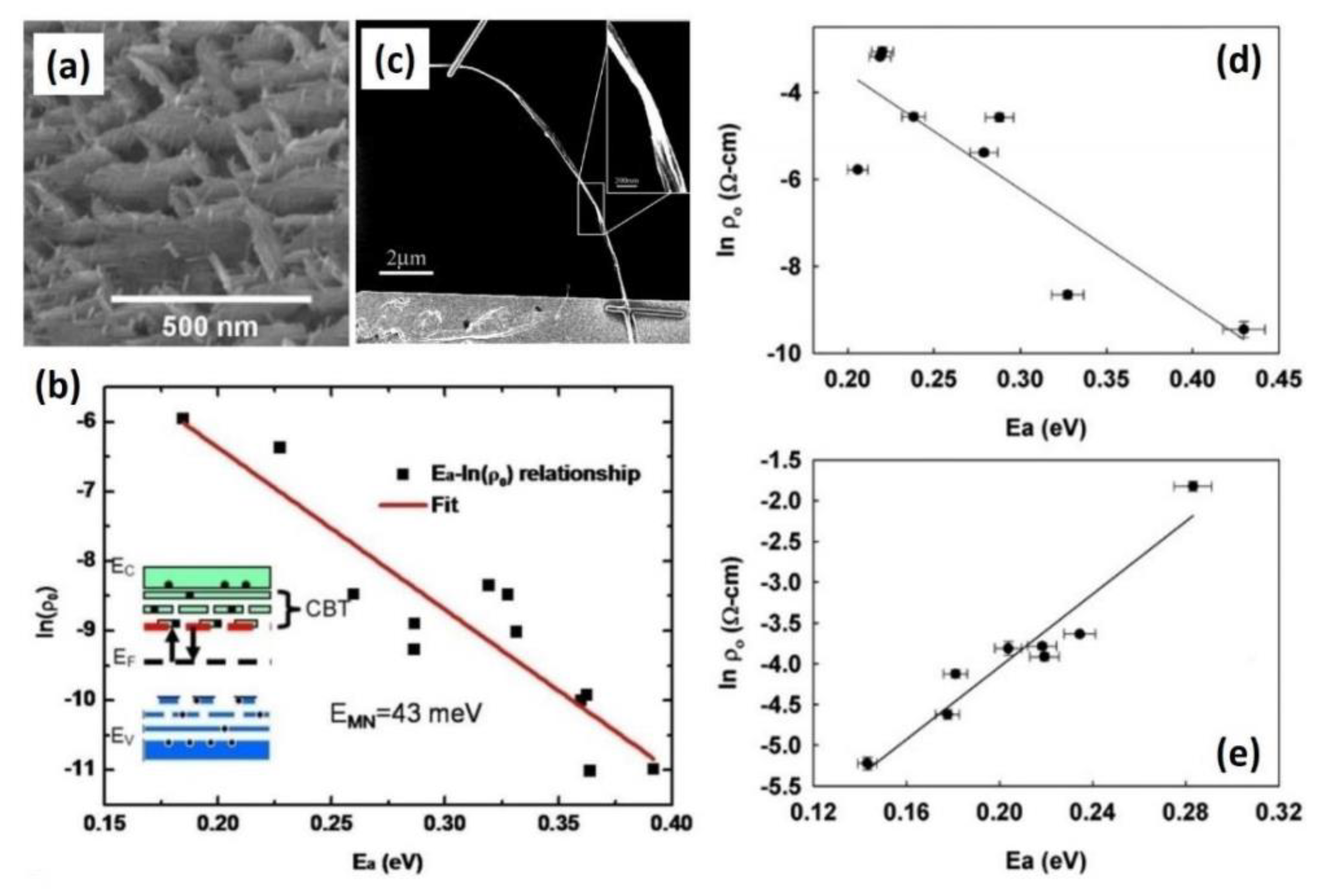
As for the thermal activation of the conduction, MNR has been found in a wide variety of thermally activated processes [13,81]. Basically, MNR is ascribed to the disorder [48], which could introduce a (large) density of localized states (traps) in material, and accordingly the EMN of the material is deemed as a measure of its disorder. MNR states generate in a thermally activated process, such as the temperature-dependence of the resistivity (ρ) of semiconductors [18]
ρ = −ρ0 exp (Ea/kT)
The increase in activation energy Ea is partially compensated by the increase in prefactor (ρ0) [18]:
where EMN is “Meyer–Neldel” energy, and ρ00 is the “intrinsic” resistivity related to the material itself. In Bi2S3 systems, MNR reveals several carrier-trapping-related transport behaviors [13,81]. In Bi2S3 nested nanonetworks (BSNNN, Figure 5a), normal MNR is observed with EMN as 43 meV, as shown in Figure 5b [81]. This is in line with the studies of single Bi2S3 nanowires, where EMN is 38 meV (see Figure 5c,d) [13,48]. However, the annealing treatment of the samples could change the positive EMN to negative (Figure 5e) [13,48]. Different MNR behaviors can be understood under the unified framework based on the trap-limited-current-based model of MNR, which could naturally produce either positive or negative EMN [48].
lnρ0 = lnρ00 + Ea/EMN
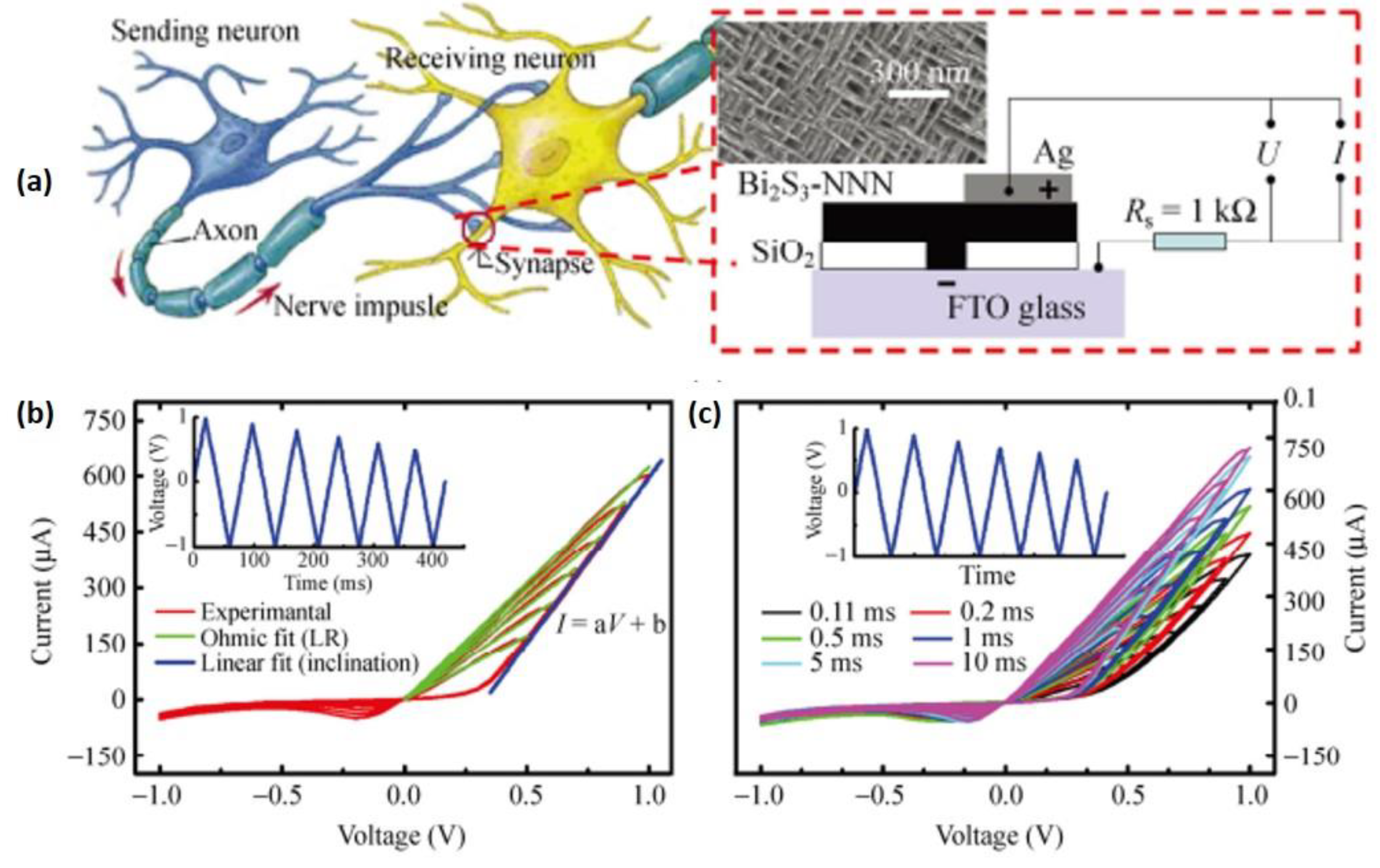
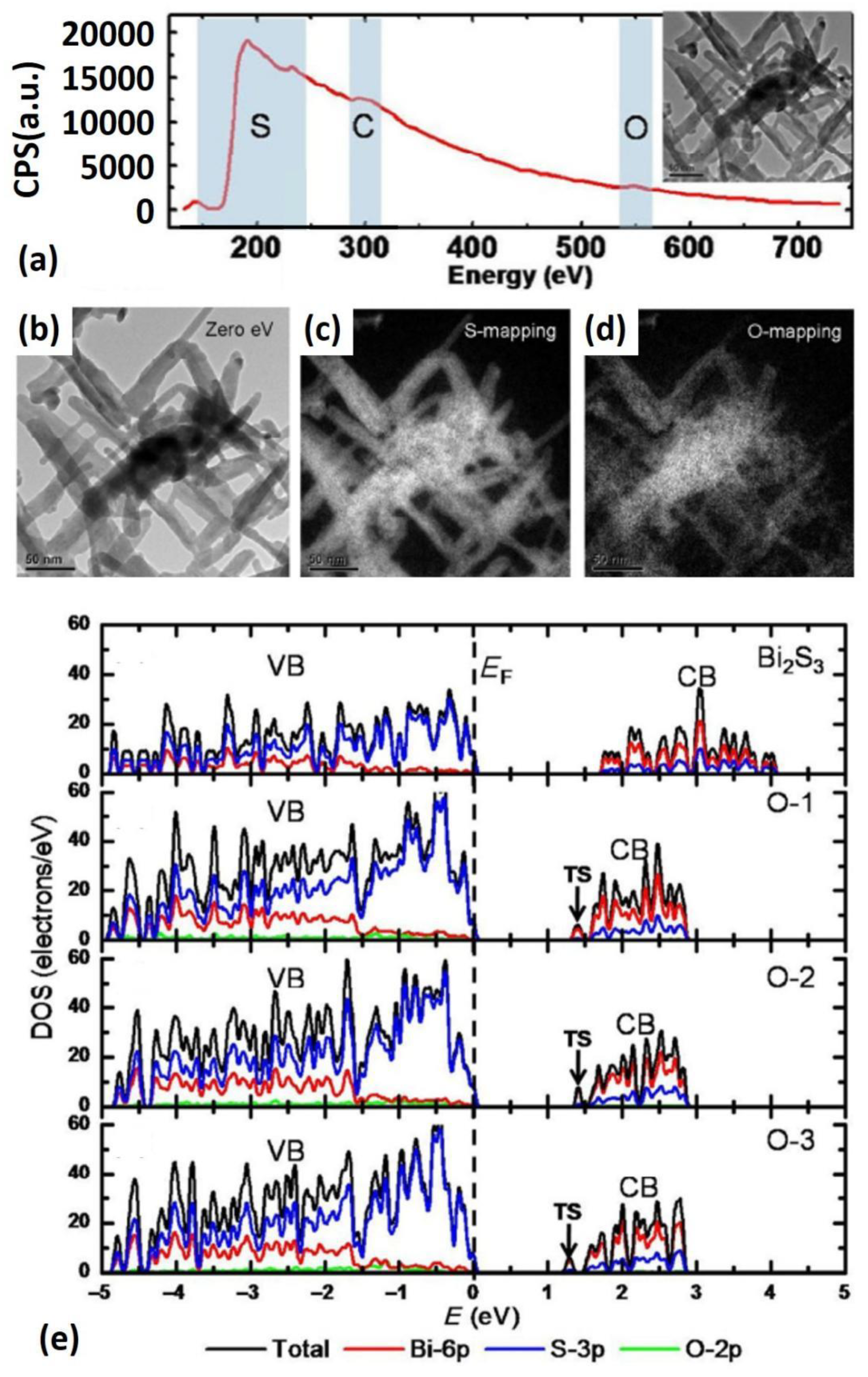
Moreover, Bi2S3 could also be resistively switchable. Specifically, the conductance of the interfaces of Pt/Bi2S3 and FTO/Bi2S3 can be bipolar switched [57]. Such bipolar switching can be highly continuous, and seems quite promising for application in memristors for neural computing, thanks to its good bivariate-continuous-tunable memristance, as shown in Figure 6 [21]. The atomic origin of such memristive features is the carrier-trapping at the interface induced by oxygen-doping [19], which is revealed by combining I–V characterization (Figure 6b,c), electron energy-loss spectroscopy (EELS, Figure 7a–d), and first-principle calculation (Figure 7e).
3.2. Optical Properties
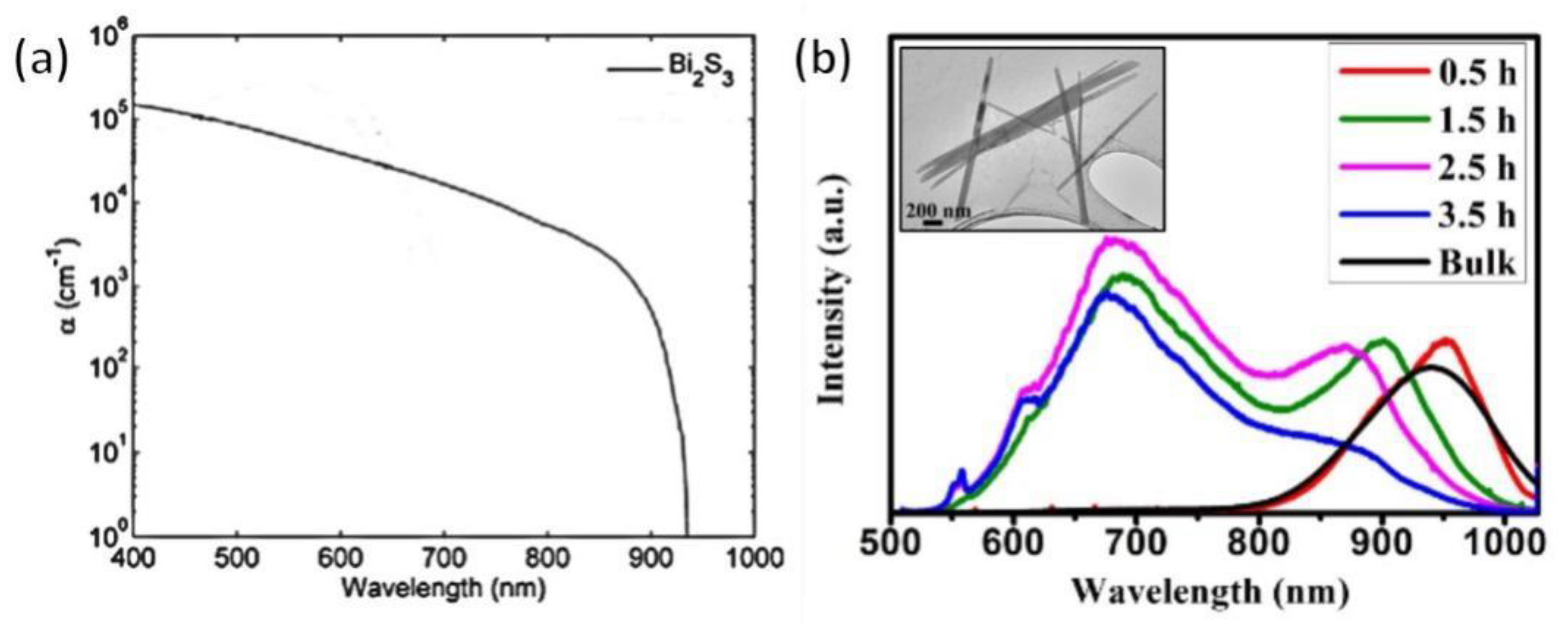
As proposed in Section 3.1, the bandgap of (bulk) Bi2S3 is ~1.3 eV, hence could produce a large absorption coefficient around near-infrared and visual range. Especially for applications such as solar energy, the high absorption coefficient of Bi2S3 in the order of 104 cm−1 enables it to serve as a highly efficient absorbing layer for sunlight, as shown in Figure 8a [27]. Such an effective absorber might be also beneficial for constructing laser thermal lithography resist [85], whose transparent level could be proportional to the laser intensity of the metal-transparent-metal-oxide system [86], while the obtained pattern might be grayscale and useful for the photomask on 3D lithography [86]. These observations agree well with the first-principle calculation of the linear optical spectra response of Bi2S3 [13], while the optical non-linearity of Bi2S3 is important due to its relationship with the control of light in optical switching devices. Typically, the three-order nonlinear coefficient χ(3) of Bi2S3 nanocrystal measured by Z-scan technique is at 1.43 × 10⁻¹¹ (esu) level [87], which is smaller than the first-principle calculated value of (bulk) Bi2S3 due to the quantum confinement effect in the nanocrystals [13].
The photoluminescence (PL) of Bi2S3 shows strong size effect, as shown in Figure 8b [24,41,88]. The studies of the samples synthesized via a high power sonication process can be taken as examples [24]: basically, the PL spectrum of bulk Bi2S3 consists of a main peak around 946 nm, which is ascribed to the band edge emission. However, as the Bi2S3 is high-power sonically treated for different durations from 0.5 h to 3.5 h, and accordingly exfoliated to van der Waals strings with different sizes [24], the emission from the Bi2S3 could show the new peak centered at 685 nm along with the initial main peak, which seems to be shifted to ~900 nm [24]. This can be attributed to the crystal defects, such as sulfur vacancies, which create deep trap states and accordingly provide alternative recombination pathways for excitonic recombination and shallowly trapped electron–hole pairs, resulting in the observed PL [24,29]. However, it is well-known that crystal defects might also increase the non-radiative recombination [89], and more physical details of the shifted-peak should be revealed by combining with other characterizations, such as absorption spectra and/or photo-carrier relaxing kinetics [90]. Further-exfoliated nanoribbons of Bi2S3 have been inserted with oxide atoms resulting in a marked reduction in the bulky band edge emission [24,29]. The CVD-grown and hydrothermal synthesized Bi2S3 nanosheet and nanorod also show similar new a PL peak around 624 nm beyond the band gap of bulk Bi2S3 [16,38]. Likewise, Bi2S3 nanoparticles prepared by reflux method could produce a PL peak near 580 nm even larger than the band gap of bulk Bi2S3 [16].
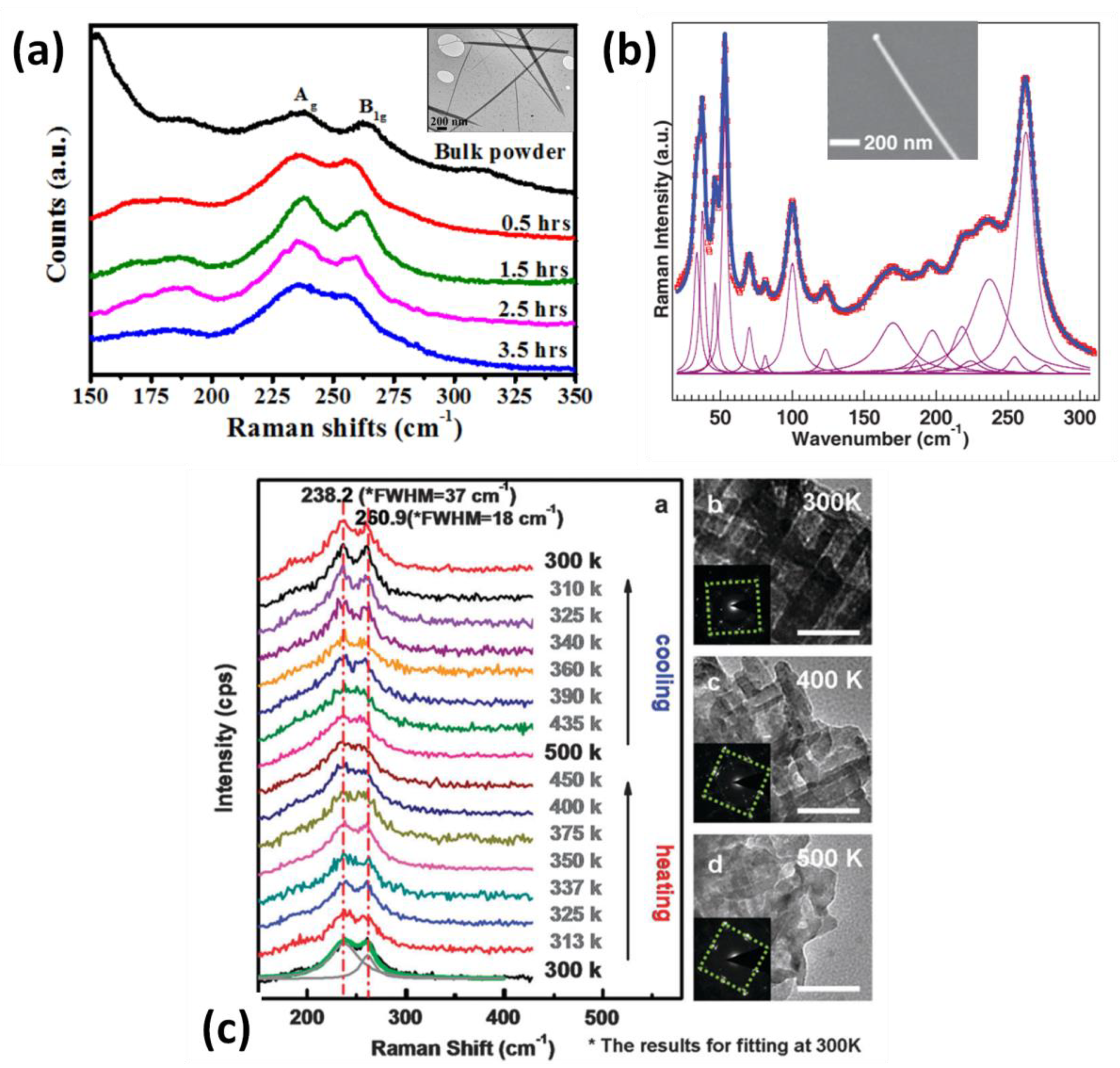
The Raman spectra of Bi2S3 mainly locates within the range of 30–300 cm−1 [78] (see Table 4). Most observed phonons are Ag and B1g modes; there are two major peaks observable in some samples (Figure 9a), which are contributed by transverse Ag mode at 237.2 cm−1 and longitudinal B1g vibration mode at 260.7 cm−1 revealed by first-principle calculation [78]. Actually, the wave number differences between the theoretical calculations and the experiment observations could be less than 5 cm−1 (Figure 9b). However, the Raman modes of the 2D nanosheets would unanimously shift toward higher wave numbers when compared with bulk Bi2S3 samples [24,29]. Such a shift can be associated with decreased long-range Coulombic interaction in few-layers nanosheets [29]. Moreover, due to the breaking of symmetry in bulk or nanostructures that can occur as a result of displacement defects in the lattice, which allows for the relaxation of Raman selection rules, some infrared (IR)-only mode could become Raman-active [78], resulting in the emergence of new peaks. Additionally, the peaks of some modes could occur with broadened FWHM, similarly to the observations in other bismuth compounds [61]. Moreover, Bi2S3 tend to be thermally oxidized by annealing [57], and therefore the laser-heating effect during Raman characterization should be carefully considered. The temperature-dependent Raman spectrum shows that the Bi2S3 nanostructure (e.g., nested nanonetwork) could be thermally -stable under 500 K [22]. However, at a higher temperature of ~573 K, thermal oxidization would occur [57], resulting in the variations of the optical properties, such as band-edge emission reduction due to oxygen-atom insertion into the 2D Bi2S3 nanosheet after long-term exfoliation [24].
4. Applications
In early years, Bi2S3 nanostructures were considered as interesting candidates for applications in fields such as thermoelectricity and light-absorption layers [31,35]. More recently, the special optical and electronic properties of Bi2S3 have appealed to applications in new fields, such as photocatalysis, photodetection, solar energy conversion, optical-switching, and biology [4,22,43,91]. As this review is concerned with the optoelectronics of nano-Bi2S3, here we mainly discuss its representative optoelectronic applications, including photodetection, solar cells and photocatalysis.
4.1. Photodetection
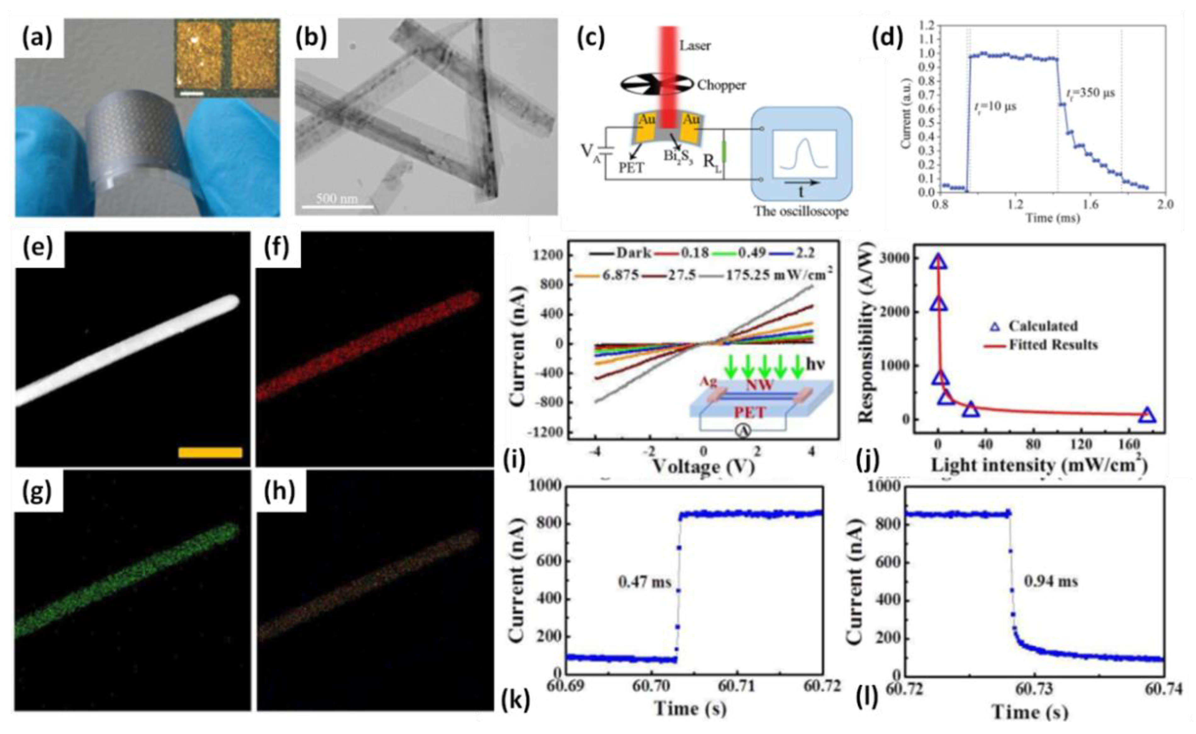
As typical binary V-VI semiconductors, bismuth chalcogenides of Bi2X3 (X = S, Se, Te) are a category of distinctive photoresponsive materials, owing to their environment-friendly chemical compositions and dramatic optical, electrical, and photoelectric conversion characteristics [3,4,22,43,91]. Among them, Bi2S3 is provided with an optimal band gap of 1.3–1.7 eV and high absorption coefficient of 104~105 cm−1 and has become a promising candidate for photodetection (Table 5) [91]. The responsive spectral range of nano-Bi2S3 for photodetection is from visible to the near-infra band [17,22]. In most cases, the on/off ratio of the nano-Bi2S3 photodetector could be higher than 100 [44,92], however, perhaps due to the existence of plentiful carrier traps, the temporal response of some samples is at the level of a few seconds [18,71,93,94], far from the requirements of real-time imaging, which uses speeds of, e.g., 30 frames per second (FPS). Rational trap-passivation by post-processing and junction barrier modification, as well as improving the crystalline quality or introducing heterogeneous structures, could markedly shorten the response time to sub-ms or even tens μs [23,50,95]. The high-quality nano-Bi2S3 flexible photodetector developed by H. Yu et.al. shows 10 μs rise time and 350 μs decay time (Figure 10a–d) [23,95]. Ref. [50] proposes a single-nanowire-device, in which Bi2S3 NW is surface-oxidated to fill the vacancies of sulfur with oxygen atoms and in situ form a Bi2S3/Bi2S3-xOx heterojunction (Figure 10e–h). Such a heterojunction could not only maintain good response time at sub-ms level at visible range, but also achieve rather high responsivity (2908.9 A/W) and detectivity (~1011 Jones), as shown in Figure 10i–l. The improvement of the overall detection performances of such a Bi2S3/Bi2S3-xOx heterojunction might be attributed to two factors: (1) the Bi2S3 and Bi2S3-xOx are n-type and p-type, respectively, and accordingly, the intrinsic electrical field of PN junction enables accelerated carrier motion [96]; (2) other than the junctions such as Bi2S3/BiOX (X = Cl, I) [21,61,71], the proposed Bi2S3/Bi2S3-xOx system has better lattice matching, which reduces the interface defects.
4.2. Photovoltaic Cell
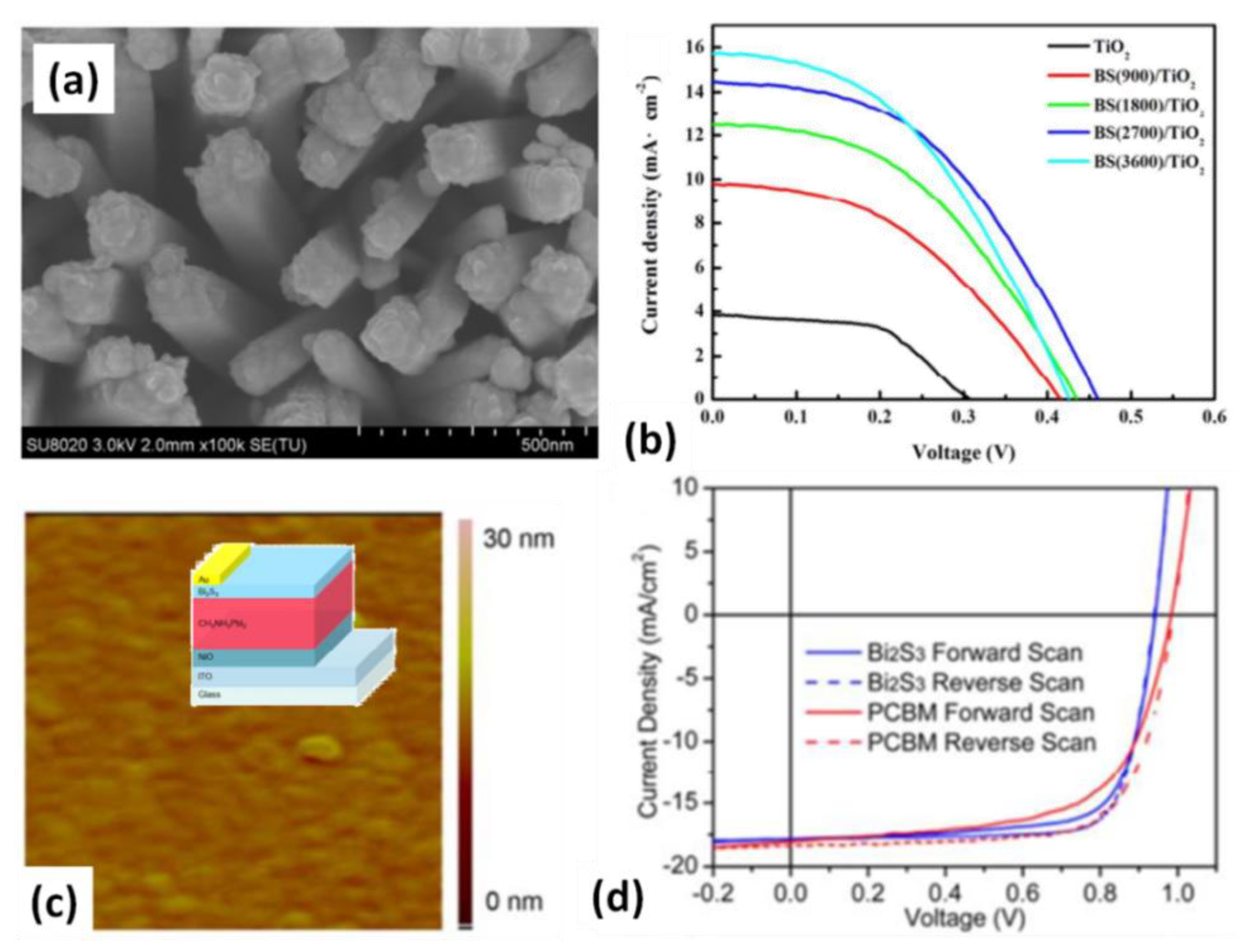
As mentioned above, Bi2S3 is a binary chalcogenide semiconductor with single phase and fixed composition. It inspires the exploration as a promising absorber material for solar energy (Table 6). This is because on one hand, its direct bandgap of 1.3~1.7 eV lies within the optimal bandgap value for the single junction solar cell, while on the other hand, Bi2S3 has a high absorption coefficient (at wavelengths of approximately 600 nm) and relatively high carrier mobility, enabling full light absorption and photogenerated carrier collection within a film thickness of, typically, a few micrometers [26]. In addition, the raw materials (Bi and S) are low-cost and non-toxic. All the above features make Bi2S3 a candidate for solar absorbers. Moreover, beyond the regular light-absorption function, nano-Bi2S3 in solar cells could serve as a number of other roles, such as the electron acceptor for organic or inorganic heterojunction solar cells, the media for dye- or quantum-dot-sensitization, and the electron transport layer for perovskite solar cells [14,26,37,45,97]. It seems that the regular PN junction structure using Bi2S3 as the n-layer cannot produce a practical performance for solar-cell application. Typical conversion efficiency is less than 1% [36,45,70,98,99,100,101,102], while state-of-art quantum dot-sensitized solar cells (QDSSCs) with Bi2S3 quantum dots could achieve conversion efficiency higher than 3% (Figure 11a,b) [14,103]. The hybridization strategy, e.g., Bi2S3 nanowire networks/P3HT hybrid solar cells, or Bi2S3/TiO2 cross-linked-structure, could further improve the conversion efficiency [37,103]. Besides its use as a conversion media, Bi2S3 could also be a promising electron transport layer for perovskite solar cells (Figure 11c); the NiO/CH3NH3PbI3/Bi2S3 system could achieve conversion efficiency of 13% (Figure 11d) [26].
Table 5.
Selected reports on the nano-Bi2S3-based photodetector.
| Samples | Wavelength | Ion/Ioff | Temporal Response (Rise/Decay) | Responsivity |
|---|---|---|---|---|
| Bi2S3 nano-networks [18] | 671 nm | / | ~3 s | / |
| Hierarchical Bi2S3 nanostructures [91] | / | / | 50/240 ms | / |
| Bi2S3/Bi2S3-xOx nanowire [50] | 475–650 nm | 44.6 | 0.47/0.93 ms | 2908.9 A/W |
| Bi2S3 nanocrystalline [47] | / | / | 23 ms | / |
| Bi2S3/BiOCl composites [99] | / | 330 | 70 ms | / |
| Bi2S3 nanorod [23,95] | 405 to 780 nm | / | 10/350 μs | 4.4 A/W |
| Bi2S3/SnS heterojunction thin film [93] | 400 to 800 nm | / | ~50 s | / |
| Bi2S3 nanorods and nanoflowers [44] | Laser@809 nm and 980 nm | ~100 | 2/3 s | / |
| Bi2S3 thin film [70] | 650 nm | / | 67.8 ms | / |
| Dandelion-shaped hierarchical Bi2S3 microsphere [92] | 650 nm | 567 | ~10 s | / |
| Bi2S3/BiOI p-n heterojunction [71] | visible | / | ~5 s | / |
| Bi2S3 Nanorods [94] | 475 nm/550 nm/650 nm | / | ~5 s | / |
To summarize the studies on nano-Bi2S3 in solar cells, this system so far seems not to have fully realized its potential. The non-practical conversion efficiency may be limited by superficial defects in the Bi2S3 [22]. In addition, on the viewpoint of material, as a semiconductor already possessing an optimal photovoltaic band gap, when Bi2S3 is processed into nanoscale, it might help to produce photon-conversion sites, but on the other hand it is also critical to avoid band-misalignment due to the unnecessary increase in the band gap brought by quantum confinement in the nanostructures [7]. Rational trade-off among different aspects, including carrier mobility, carrier concentration, photon-conversion site (area of junction for electron-hole pair generation and separation), and band alignment would be quite critical for the further progress of the nano-Bi2S3-based solar cell.
4.3. Photocatalysis
Photocatalysis is one of most active research fields focused on the applications of Bi2S3 nanostructures, with hundreds of reports published within a few years [16,69,105]. The interest in this field is based in particular on the low cost and low toxicity of Bi, which has been named “green metal” by some authors, as well as its several compounds, including Bi2S3 [58,61,74]. Table 7 presents a selection of references where the photocatalytic properties of Bi2S3-based materials were studied, and specifies the chemical reactions that were considered.
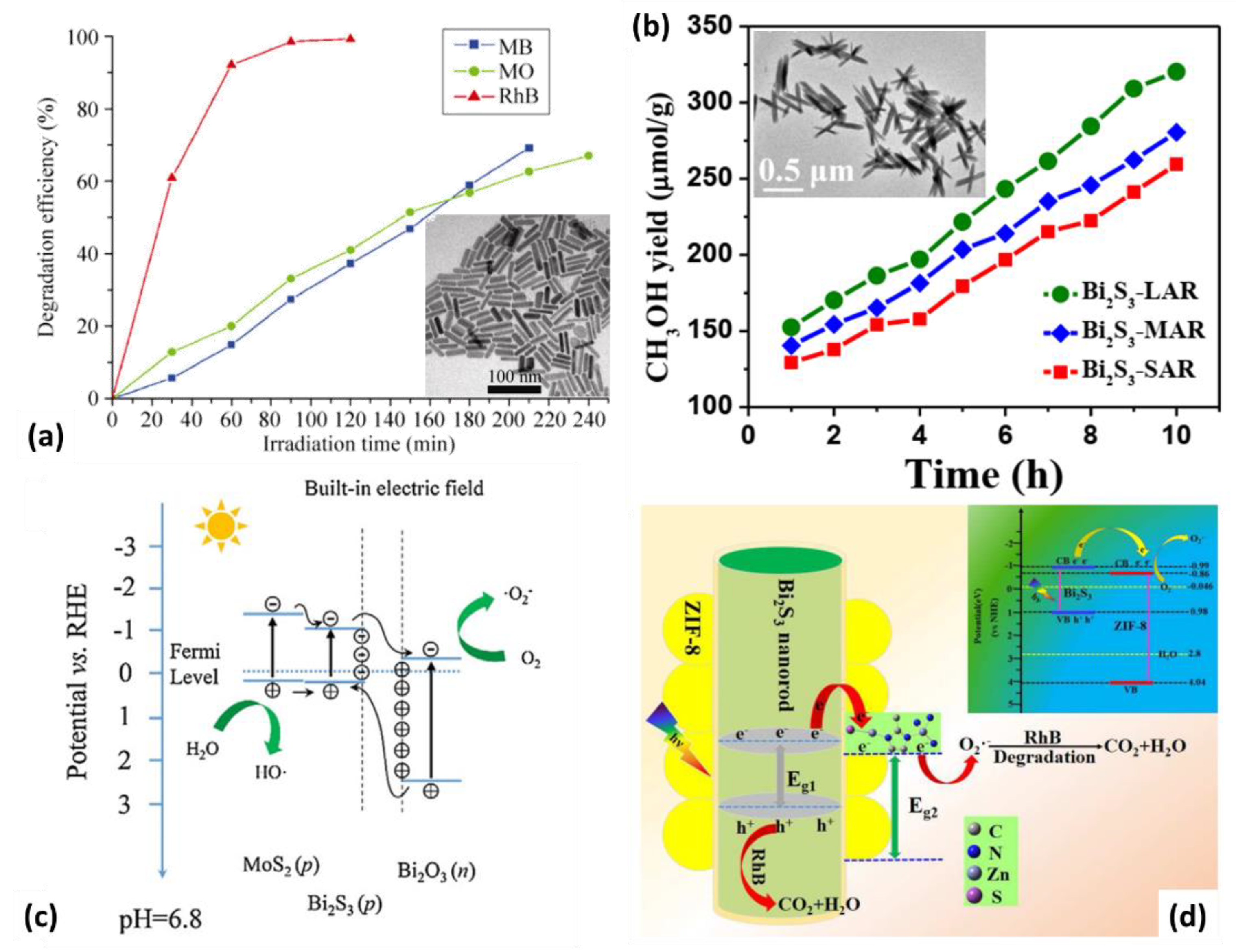
The pioneering works on this topic demonstrated that Bi2S3 nanostructures can act as direct photocatalysts [4,69]. In [69], solution-processed Bi nanowires diluted in water were used as the catalyst for RhB removal. A solution of RhB was degraded under visible light within 4 h. Afterward, the degradation of MO and MB was also demonstrated (Figure 12a) [4]. Besides the exploration on dye-removal, nano-Bi2S3 (nanoparticles, microspheres, thin urchin-like Bi2S3 spheres, and nanoribbon) was also able to reduce CO2 to methyl and methanol (Figure 12b) [58,59]. As mentioned above, Bi2S3 nanostructures efficiently adsorb the incident light, which can be converted to photocarriers that migrate to the nanostructure surface, hence they can ease the formation of intermediates, accelerating chemical reactions. Thus, the high absorption capability of Bi2S3 certainly plays a key role in this process, because it enables a significant optical absorption efficiency that is required for the efficient generation of photocarriers. Moreover, other than the ~1.3 eV band gap of bulk Bi2S3, the nano-structured Bi2S3 could have varied band structure, and accordingly achieve tunable photocatalytic response spectral range under visible light and also UV [4,69]. Furthermore, it is noteworthy that the potential of the photogenerated electrons (holes) must be low (high) enough so that they can efficiently trigger the chemical reaction of interest, and this potential is defined by the photon energy of the incident photons. Hence, the hybrid structure of other materials (TiO2, Bi2WO6, Bi2O2CO3 Bi2O3, ZIF-8, ZnS, CuS) with nano-Bi2S3 could enhance catalysis performances. Accordingly, the co-catalysis by such hybrid structures seems more promising for the degradation of RhB, CV, MO, MB, and ofloxacin [52,58,71,72,73,74,77].
The photocatalysis mechanism of nano-Bi2S3 suggested by experimental results varied from one work to another (together with the nature and structure of the hybrid material), however, some evidence highlighted in these studies can be extracted. On one hand, Bi2S3 nanostructures allow photocatalytic capabilities in the visible region due to their rational band gap and strong optical absorption efficiency. On the other hand, depending on the electronic configuration of the hybrid (including the potential of the photocarriers in Bi2S3 nanostructure, location of the conduction, and valence band of the semiconductor), photocarriers, especially electrons, can flow from the Bi2S3 nanostructure to the hybrid semiconductor or the opposite. In other words, according to these different reports, nano-Bi2S3 can act as an electron donor (the electrons being made available for reactions at the surface of the semiconductor, Figure 12c) or as electron acceptor (the electrons provided by the semiconductor reacting at their surface, Figure 12d) [49,52,73]. Thus, further studies would be of significance to understand the mechanism of the photocatalyst based on nano-Bi2S3, as well as related hybrid structures.
5. Conclusions and Perspectives
Bi2S3 has motivated and attracted the interest of scientists during the past decades due to its potential in thermoelectric and hydrogen storage and its Li- and Na- ion battery properties. Furthermore, Bi2S3 has recently become appealing for applications involving its particular optoelectronic properties. Increasing interest has been paid especially to its application in photodetection, solar energy conversion, and photocatalysts. In this article, we present a comprehensive review of the recent advances on this field: electrical and optical properties of Bi2S3, growth of Bi2S3 nanostructures, and emerging optoelectronic applications. Bi2S3 nanostructures with a broad variety of sizes and shapes can be prepared with different existing fabrication methods:
- (1)
- Vapor phase deposition, involving thermal evaporation, LP-MOCVD, and PLD; mainly used to prepare thin film.
- (2)
- Liquid phase deposition, involving chemical bath or electrochemical deposition, is also used to fabricate thin film.
- (3)
- Surface sulfurization can produce nano-Bi2S3 with better crystalline quality, but requires high processing temperature.
- (4)
- Chemical synthesis Bi2S3 nanostructures with a broad variety of shapes from 0D to 3D, as well as the hierarchical and heterogeneous structures of Bi2S3.
Optimal band gap, high light absorption, and good carrier mobility concentration make nano-Bi2S3 feasible for a series of optoelectronic applications, but better controlled crystalline quality, nanostructure size, shape, and environment is desired. The SOC effects could be critical to further extend the design space of the (linear) optical response, while rational doping could help to improve the nonlinear optical properties and consequently produce more promising nonlinear optical materials [13]. However, there are still amount of works to achieve better nano-Bi2S3 optoelectronics. In most of the works that we have discussed, the influence of the crystal facets exposed at the surface of the Bi2S3 nanostructures on their optoelectronic functionalities has not been thoroughly evaluated. In addition, because of the structural and electronic anisotropy of nano-Bi2S3 and its facet-dependent surface states [29], the nature of the exposed facets might affect either the optical response of nano-Bi2S3 with a high surface-to-volume ratio (where surface states play a significant role on the overall response) or their functionalities for applications in which surfaces are a key player (such as catalysis, surface-enhanced Raman spectroscopy, and charge transport). However, emerging photodetector, solar cells, and photocatalysts based on nano-Bi2S3 clearly show great potential in optoelectronics. Besides these applications, further opportunities for nano-Bi2S3 in this field may lie in the switchable optical device, the bolometer, and beyond [85].
In sum, the progress on the fabrication of Bi2S3 nanostructures, the control and understanding of their excellent optoelectronic responses, and the emergence of alternative applications open new possibilities for nano-Bi2S3 beyond the already-explored paths. More experimental observations are needed to realize its optical potential. Further developments are also necessary to overcome the obstacles and highlight the unsolved issues to achieve more practical nano Bi2S3-based optical materials and devices.
Author Contributions
Conceptualization, Y.T. and Z.L.; writing—original draft preparation, Y.T.; writing—review and editing, Y.T. and Z.L. All authors have read and agreed to the published version of the manuscript.
Funding
This research was supported by the Scientific Research Fund of Hunan Provincial Education Department (No.20C0367, No.19B100) and Hunan Provincial Natural Science Fund (2019JJ50025).
Data Availability Statement
All data included in this study are available upon request by contact with the corresponding author.
Conflicts of Interest
The authors declare no conflict of interest.
References
- Popescu, M. Chalcogenides—Past, present, future. J. Non-Cryst. Solids 2006, 352, 887–891. [Google Scholar] [CrossRef]
- Sousa, V. Chalcogenide materials and their application to Non-Volatile Memories. Microelectron. Eng. 2011, 88, 807–813. [Google Scholar] [CrossRef]
- Moore, J.E. The birth of topological insulators. Nature 2010, 464, 194–198. [Google Scholar] [CrossRef] [PubMed]
- Wu, T.; Zhou, X.; Zhang, H.; Zhong, X. Bi2S3 nanostructures: A new photocatalyst. Nano Res. 2010, 3, 379–386. [Google Scholar] [CrossRef] [Green Version]
- Sanghera, J.S.; Shaw, L.B.; Aggarwal, I.D. Chalcogenide Glass-Fiber-Based Mid-IR Sources and Applications. IEEE J. Sel. Top. Quantum Electron. 2009, 15, 114–119. [Google Scholar] [CrossRef]
- Toudert, J.; Serna, R. Interband transitions in semi-metals, semiconductors, and topological insulators: A new driving force for plasmonics and nanophotonics [Invited]. Opt. Mater. Express 2017, 7, 2299–2325. [Google Scholar] [CrossRef]
- Tian, Y.; Toudert, J. Nanobismuth: Fabrication, Optical, and Plasmonic Properties—Emerging Applications. J. Nanotechnol. 2018, 2018, 3250932. [Google Scholar] [CrossRef] [Green Version]
- Panmand, R.P.; Kulkarni, M.V.; Valant, M.; Gosavi, S.W.; Kale, B.B. Quantum confinement of Bi2S3 in glass with magnetic behavior. AIP Adv. 2013, 3, 022123. [Google Scholar] [CrossRef]
- Yang, Y.; Xu, Z.; Sheng, L.; Shen, R.; Xing, D.Y. Magnetoresistance in an ultrathin Bi2Se3 film between two ferromagnetic insulators. Appl. Phys. Lett. 2011, 99, 182101. [Google Scholar] [CrossRef]
- Lu, C.; Li, Z.; Yu, L.; Zhang, L.; Xia, Z.; Jiang, T.; Yin, W.; Dou, S.; Liu, Z.; Sun, J. Nanostructured Bi2S3 encapsulated within three-dimensional N-doped graphene as active and flexible anodes for sodium-ion batteries. Nano Res. 2018, 11, 4614–4626. [Google Scholar] [CrossRef]
- Zhao, Y.; Gao, D.; Ni, J.; Gao, L.; Yang, J.; Dongliang, Y. One-pot facile fabrication of carbon-coated Bi2S3 nanomeshes with efficient Li-storage capability. Nano Res. 2014, 7, 765–773. [Google Scholar] [CrossRef]
- Chang, Y.; Yang, Q.L.; Guo, J.; Feng, J.; Ge, Z.H. Enhanced thermoelectric properties of Bi2S3 polycrystals through an electroless nickel plating process. RSC Adv. 2019, 9, 23029–23035. [Google Scholar] [CrossRef] [PubMed] [Green Version]
- Ben Abdallah, H.; Ouerghui, W. Spin–orbit coupling effect on electronic, linear and nonlinear optical properties of Bi2S3 and the ternary bismuth sulfide Bi2S2.75Se0.25: Ab-initio calculations. Opt. Quantum Electron. 2021, 54, 20. [Google Scholar] [CrossRef]
- Han, M.; Guo, H.; Li, B.; Jia, J.; Wang, W. Controllable coverage of Bi2S3 quantum dots on one-dimensional TiO2 nanorod arrays by pulsed laser deposition technique for high photoelectrochemical properties. New J. Chem. 2017, 41, 4820–4827. [Google Scholar] [CrossRef]
- Arabzadeh, A.; Salimi, A. Facile Synthesis of Ultra-wide Two Dimensional Bi2S3 Nanosheets: Characterizations, Properties and Applications in Hydrogen Peroxide Sensing and Hydrogen Storage. Electroanalysis 2017, 29, 2027–2035. [Google Scholar] [CrossRef]
- Arumugam, J.; Raj, A.D.; Irudayaraj, A.A. Solvent effects on the properties of Bi2S3 nanoparticles: Photocatalytic application. J. Mater. Sci. Mater. Electron. 2017, 28, 3487–3494. [Google Scholar] [CrossRef]
- Chitara, B.; Kolli, B.S.; Yan, F. Near-Infrared Photodetectors Based on 2D Bi2S3. Chem. Phys. Lett. 2022, 804, 139876. [Google Scholar] [CrossRef]
- Tian, Y.; Zhang, S.; Tan, W. Improved optical and electrical switching in Bi2S3 nested nano-networks with broad trap distribution. Appl. Nanosci. 2022, 12, 2023–2030. [Google Scholar] [CrossRef]
- Tian, Y.; Pan, L.; Guo, C.F.; Liu, Q. Atomic origin of the traps in memristive interface. Nano Res. 2017, 10, 1924–1931. [Google Scholar] [CrossRef]
- Schricker, A.D.; Sigman, M.B., Jr.; Korgel, B.A. Electrical transport, Meyer–Neldel rule and oxygen sensitivity of Bi2S3 nanowires. Nanotechnology 2005, 16, S508. [Google Scholar] [CrossRef]
- Stallinga, P.; Gomes, H. Trap states as an explanation for the Meyer–Neldel rule in semiconductors. Org. Electron. 2005, 6, 137–141. [Google Scholar] [CrossRef]
- Tian, Y.; Guo, C.; Guo, S.; Yu, T.; Liu, Q. Bivariate-continuous-tunable interface memristor based on Bi2S3 nested nano-networks. Nano Res. 2014, 7, 953–962. [Google Scholar] [CrossRef]
- Tian, Y.; Guo, C.F.; Zhang, J.; Liu, Q. Operable persistent photoconductivity of Bi2S3 nested nano-networks. Phys. Chem. Chem. Phys. 2015, 17, 851–857. [Google Scholar] [CrossRef] [PubMed]
- Schricker, A.D. Electrical Properties of Single GaAs, Bi2S3 and Ge Nanowires; University of Texas Libraries: San Antonio, TX, USA, 2005. [Google Scholar]
- Yu, H.; Wang, J. Bismuth Sulfide (Bi2S3) Nanorods as Efficient Photodetection Materials. In Proceedings of the 2016 5th International Conference on Advanced Materials and Computer Science, Qingdao, China, 26–27 March; pp. 935–938.
- Dhar, N.; Syed, N.; Mohiuddin, M.; Jannat, A.; Zavabeti, A.; Zhang, B.Y.; Datta, R.S.; Atkin, P.; Mahmood, N.; Esrafilzadeh, D.; et al. Exfoliation Behavior of van der Waals Strings: Case Study of Bi2S3. ACS Appl. Mater. Interfaces 2018, 10, 42603–42611. [Google Scholar] [CrossRef] [PubMed]
- Guo, C.; Zhang, J.; Tian, Y.; Liu, Q. A General Strategy to Superstructured Networks and Nested Self-Similar Networks of Bismuth Compounds. ACS Nano 2012, 6, 8746–8752. [Google Scholar] [CrossRef]
- Li, D.-B.; Hu, L.; Xie, Y.; Niu, G.; Liu, T.; Zhou, Y.; Gao, L.; Yang, B.; Tang, J. Low-Temperature-Processed Amorphous Bi2S3 Film as an Inorganic Electron Transport Layer for Perovskite Solar Cells. ACS Photonics 2016, 3, 2122–2128. [Google Scholar] [CrossRef]
- Martinez, L.; Bernechea, M.; de Arquer, F.P.G.; Konstantatos, G. Near IR-Sensitive, Non-toxic, Polymer/Nanocrystal Solar Cells Employing Bi2S3 as the Electron Acceptor. Adv. Energy Mater. 2011, 1, 1029–1035. [Google Scholar] [CrossRef]
- Li, L.; Sun, N.; Huang, Y.; Qin, Y.; Zhao, N.; Gao, J.; Li, M.; Zhou, H.; Qi, L. Topotactic Transformation of Single-Crystalline Precursor Discs into Disc-Like Bi2S3 Nanorod Networks. Adv. Funct. Mater. 2008, 18, 1194–1201. [Google Scholar] [CrossRef]
- Messalea, K.A.; Zavabeti, A.; Mohiuddin, M.; Syed, N.; Jannat, A.; Atkin, P.; Ahmed, T.; Walia, S.; McConville, C.F.; Kalantar-Zadeh, K.; et al. Two-Step Synthesis of Large-Area 2D Bi2S3 Nanosheets Featuring High In-Plane Anisotropy. Adv. Mater. Interfaces 2020, 7, 2001131. [Google Scholar] [CrossRef]
- Chen, X.L.; Yan, K.; Chu, H.Y. Preheating Effects on Bi2S3 Morphology Synthesized via Hydrothermal Method. Adv. Mater. Res. 2013, 631–632, 298–302. [Google Scholar] [CrossRef]
- Wang, Z.J.; Qu, S.C.; Xu, Y.; Chen, Y.H.; Zeng, X.B.; Liu, J.P.; Wu, J.; Wang, Z.G. Solventless Synthesis of Bi2S3 Nanowires and their Application to Solar Cells. Adv. Mater. Res. 2007, 26–28, 601–607. [Google Scholar] [CrossRef]
- Reynoso, Y.R.; Martinez-Ayala, A.; Pal, M.; Paraguay-Delgado, F.; Mathews, N. Bi2S3 nanoparticles by facile chemical synthesis: Role of pH on growth and physical properties. Adv. Powder Technol. 2018, 29, 3561–3568. [Google Scholar] [CrossRef]
- Gao, C.; Shen, H.; Sun, L. Preparation of nanowall Bi2S3 films by chemical bath deposition. Appl. Surf. Sci. 2011, 258, 89–92. [Google Scholar] [CrossRef]
- Maria, C.C.S.; Patil, R.A.; Hasibuan, D.P.; Saragih, C.S.; Lai, C.-C.; Liou, Y.; Ma, Y.-R. White-light photodetection enhancement and thin film impediment in Bi2S3 nanorods/thin-films homojunction photodetectors. Appl. Surf. Sci. 2022, 584, 152608. [Google Scholar] [CrossRef]
- Chen, Y.; Wang, D.; Zhou, Y.; Pang, Q.; Shao, J.; Wang, G.; Wang, J.; Zhao, L.-D. Enhancing the thermoelectric performance of Bi2S3: A promising earth-abundant thermoelectric material. Front. Phys. 2018, 14, 13601. [Google Scholar] [CrossRef]
- Bernechea, M.; Cao, Y.; Konstantatos, G. Size and bandgap tunability in Bi2S3 colloidal nanocrystals and its effect in solution processed solar cells. J. Mater. Chem. A 2015, 3, 20642–20648. [Google Scholar] [CrossRef]
- Whittaker-Brooks, L.; Gao, J.; Hailey, A.K.; Thomas, C.R.; Yao, N.; Loo, Y.L. Bi2S3 nanowire networks as electron acceptor layers in solution-processed hybrid solar cells. J. Mater. Chem. C 2015, 3, 2686–2692. [Google Scholar] [CrossRef]
- Peter, L.M.; Wijayantha, K.U.; Riley, D.J.; Waggett, J.P. Band-edge tuning in self-assembled layers of Bi2S3 nanoparticles used to photosensitize nanocrystalline TiO2. J. Phys. Chem. B 2003, 107, 8378–8381. [Google Scholar] [CrossRef]
- Yu, Y.; Jin, C.H.; Wang, R.H.; Chen, Q.; Peng, L.M. High-Quality Ultralong Bi2S3 Nanowires: Structure, Growth, and Properties. J. Phys. Chem. B 2005, 109, 18772–18776. [Google Scholar] [CrossRef]
- Bhattacharya, R.; Pramanik, P. Semiconductor Liquid Junction Solar Cell Based on Chemically Deposited Bi2S3 Thin Film and Some Semiconducting Properties of Bismuth Chalcogenides. J. Electrochem. Soc. 1982, 129, 332–335. [Google Scholar] [CrossRef]
- Huang, J.F.; Wang, Y.; Cao, L.Y.; Zhu, H.; Zeng, X.R. Effects of pH Value on the Structures and Optical Properties of Bi2S3 Thin Films. Key Eng. Mater. 2010, 434–435, 397–399. [Google Scholar] [CrossRef]
- Desai, J.D.; Lokhande, C.D. Nonaqueous chemical bath deposition of Bi2S3 thin films. Mater. Chem. Phys. 1993, 34, 313–316. [Google Scholar] [CrossRef]
- Yu, Y.; Sun, W.-T. Uniform Bi2S3 nanowires: Structure, growth, and field-effect transistors. Mater. Lett. 2009, 63, 1917–1920. [Google Scholar] [CrossRef]
- Chao, J.; Xing, S.; Liu, Z.; Zhang, X.; Zhao, Y.; Zhao, L.; Fan, Q. Large-scale synthesis of Bi2S3 nanorods and nanoflowers for flexible near-infrared laser detectors and visible light photodetectors. Mater. Res. Bull. 2018, 98, 194–199. [Google Scholar] [CrossRef]
- Li, Y.; Zhang, Y.; Lei, Y.; Li, P.; Jia, H.; Hou, H.; Zheng, Z. In situ fabrication of Bi2S3 nanocrystal film for photovoltaic devices. Mater. Sci. Eng. B 2012, 177, 1764–1768. [Google Scholar] [CrossRef]
- Liu, W.; Guo, C.F.; Yao, M.; Lan, Y.; Zhang, H.; Zhang, Q.; Chen, S.; Opeil, C.P.; Ren, Z. Bi2S3 nanonetwork as precursor for improved thermoelectric performance. Nano Energy 2014, 4, 113–122. [Google Scholar] [CrossRef]
- Konstantatos, G.; Levina, L.; Tang, J.; Sargent, E.H. Sensitive solution-processed Bi2S3 nanocrystalline photodetectors. Nano Lett. 2008, 8, 4002–4006. [Google Scholar] [CrossRef]
- He, D.; Wang, Y.; Song, S.; Liu, S.; Luo, Y.; Deng, Y. Polymer-based nanocomposites employing Bi2S3@SiO2 nanorods for high dielectric performance: Understanding the role of interfacial polarization in semiconductor-insulator core-shell nanostructure. Compos. Sci. Technol. 2017, 151, 25–33. [Google Scholar] [CrossRef]
- Ding, Y.H.; Zhang, X.L.; Zhang, N.; Zhang, J.Y.; Zhang, R.; Liu, Y.F.; Fang, Y.Z. A visible-light driven Bi2S3@ZIF-8 core–shell heterostructure and synergistic photocatalysis mechanism. Dalton Trans. 2018, 47, 684–692. [Google Scholar] [CrossRef]
- Errando-Herranz, C.; Takabayashi, A.Y.; Edinger, P.; Sattari, H.; Gylfason, K.B.; Quack, N. MEMS for Photonic Integrated Circuits. IEEE J. Sel. Top. Quantum Electron. 2020, 26, 1–16. [Google Scholar] [CrossRef]
- Xie, Y.-Y.; Ni, P.-N.; Wang, Q.-H.; Kan, Q.; Briere, G.; Chen, P.-P.; Zhao, Z.-Z.; Delga, A.; Ren, H.-R.; Chen, H.-D.; et al. Metasurface-integrated vertical cavity surface-emitting lasers for programmable directional lasing emissions. Nat. Nanotechnol. 2020, 15, 125–130. [Google Scholar] [CrossRef] [PubMed] [Green Version]
- Rife, J.C.; Miller, M.M.; Sheehan, P.E.; Tamanaha, C.R.; Tondra, M.; Whitman, L.J. Design and performance of GMR sensors for the detection of magnetic microbeads in biosensors. Sens. Actuators A Phys. 2003, 107, 209–218. [Google Scholar] [CrossRef]
- Monteiro, O.C.; Trindade, T.; Park, J.-H.; O’Brien, P. The LP-MOCVD of CdS/Bi2S3 bilayers using single-molecule precursors. Mater. Lett. 2004, 58, 119–122. [Google Scholar] [CrossRef]
- Tian, Y.; Zhang, S.; Tan, W. Oxygen-doping to Bi2S3 thin film and its substrate-dependent resistive switching. Mater. Res. Express 2019, 6, 116324. [Google Scholar] [CrossRef]
- Jin, J.; He, T. Facile synthesis of Bi2S3 nanoribbons for photocatalytic reduction of CO2 into CH3OH. Appl. Surf. Sci. 2017, 394, 364–370. [Google Scholar] [CrossRef]
- Ma, J.; Yang, J.; Jiao, L.; Wang, T.; Lian, J.; Duan, X.; Zheng, W. Bi2S3 nanomaterials: Morphology manipulation and related properties. Dalton Trans. 2011, 40, 10100–10108. [Google Scholar] [CrossRef]
- Dong, Y.; Hu, M.; Zhang, Z.; Zapien, J.A.; Wang, X.; Lee, J.-M. Hierarchical self-assembled Bi2S3 hollow nanotubes coated with sulfur-doped amorphous carbon as advanced anode materials for lithium ion batteries. Nanoscale 2018, 10, 13343–13350. [Google Scholar] [CrossRef]
- Tian, Y.; Guo, C.F.; Guo, Y.; Wang, Q.; Liu, Q. BiOCl nanowire with hierarchical structure and its Raman features. Appl. Surf. Sci. 2012, 258, 1949–1954. [Google Scholar] [CrossRef]
- Saitou, M.; Yamaguchi, R.; Oshikawa, W. Novel process for electrodeposition of Bi2S3 thin films. Mater. Chem. Phys. 2002, 73, 306–309. [Google Scholar] [CrossRef] [Green Version]
- Mane, R.; Sankapal, B.; Lokhande, C. A chemical method for the deposition of Bi2S3 thin films from a non-aqueous bath. Thin Solid Film. 2000, 359, 136–140. [Google Scholar] [CrossRef]
- Chai, W.; Yang, F.; Yin, W.; You, S.; Wang, K.; Ye, W.; Rui, Y.; Tang, B. Bi2S3/C nanorods as efficient anode materials for lithium-ion batteries. Dalton Trans. 2019, 48, 1906–1914. [Google Scholar] [CrossRef] [PubMed]
- Zhao, G.-Q.; Zheng, Y.-J.; He, Z.-G.; Lu, Z.-X.; Wang, L.; Li, C.-F.; Jiao, F.-P.; Deng, C.-Y. Synthesis of Bi2S3 microsphere and its efficient photocatalytic activity under visible-light irradiation. Trans. Nonferrous Met. Soc. China 2018, 28, 2002–2010. [Google Scholar] [CrossRef]
- Chen, J.; Qin, S.; Song, G.; Xiang, T.; Xin, F.; Yin, X. Shape-controlled solvothermal synthesis of Bi2S3 for photocatalytic reduction of CO2 to methyl formate in methanol. Dalton Trans. 2013, 42, 15133–15138. [Google Scholar] [CrossRef] [PubMed]
- Liu, S.; Cai, Z.; Zhou, J.; Pan, A.; Liang, S. Chrysanthemum-like Bi2S3 nanostructures: A promising anode material for lithium-ion batteries and sodium-ion batteries. J. Alloys Compd. 2017, 715, 432–437. [Google Scholar] [CrossRef]
- Yan, X.; Gu, Y.; Li, C.; Zheng, B.; Li, Y.; Zhang, T.; Zhang, Z.; Yang, M. Morphology-controlled synthesis of Bi2S3 nanorods-reduced graphene oxide composites with high-performance for electrochemical detection of dopamine. Sens. Actuators B Chem. 2018, 257, 936–943. [Google Scholar] [CrossRef]
- Luo, Y.; Chen, H.; Li, X.; Gong, Z.; Wang, X.; Peng, X.; He, M.; Sheng, Z. Wet chemical synthesis of Bi2S3 nanorods for efficient photocatalysis. Mater. Lett. 2013, 105, 12–15. [Google Scholar] [CrossRef]
- Song, H.; Zhan, X.; Li, D.; Zhou, Y.; Yang, B.; Zeng, K.; Zhong, J.; Miao, X.; Tang, J. Rapid thermal evaporation of Bi2S3 layer for thin film photovoltaics. Sol. Energy Mater. Sol. Cells 2016, 146, 1–7. [Google Scholar] [CrossRef]
- Li, L.; Liu, Y.; Dai, J.Y.; Zhu, H.X.; Hong, A.J.; Zhou, X.H.; Ren, Z.F.; Liu, J.M. Thermoelectric property studies on CuxBi2SeS2 with nano-scale precipitates Bi2S3. Nano Energy 2015, 12, 447–456. [Google Scholar] [CrossRef] [Green Version]
- Ke, J.; Liu, J.; Sun, H.; Zhang, H.; Duan, X.; Liang, P.; Li, X.; Tade, M.O.; Liu, S.; Wang, S. Facile assembly of Bi2O3/Bi2S3/MoS2 n-p heterojunction with layered n-Bi2O3 and p-MoS2 for enhanced photocatalytic water oxidation and pollutant degradation. Appl. Catal. B Environ. 2017, 200, 47–55. [Google Scholar] [CrossRef]
- Wang, Q.; Liu, Z.; Feng, H.; Jin, R.; Zhang, S.; Gao, S. Engineering Bi2S3/BiOI p-n heterojunction to sensitize TiO2 nanotube arrays photoelectrodes for highly efficient solar cells and photocatalysts. Ceram. Int. 2019, 45, 3995–4002. [Google Scholar] [CrossRef]
- Adhikari, S.; Kim, D.-H. Synthesis of Bi2S3/Bi2WO6 hierarchical microstructures for enhanced visible light driven photocatalytic degradation and photoelectrochemical sensing of ofloxacin. Chem. Eng. J. 2018, 354, 692–705. [Google Scholar] [CrossRef]
- Wu, Z.; Chen, L.; Xing, C.; Jiang, D.; Xie, J.; Chen, M. Controlled synthesis of Bi2S3/ZnS microspheres by an in situ ion-exchange process with enhanced visible light photocatalytic activity. Dalton Trans. 2013, 42, 12980–12988. [Google Scholar] [CrossRef] [PubMed]
- Liang, N.; Zai, J.; Xu, M.; Zhu, Q.; Wei, X.; Qian, X. Novel Bi2S3/Bi2O2CO3 heterojunction photocatalysts with enhanced visible light responsive activity and wastewater treatment. J. Mater. Chem. A 2014, 2, 4208–4216. [Google Scholar] [CrossRef]
- Zeng, Q.; Bai, J.; Li, J.; Li, Y.; Li, X.; Zhou, B. Combined nanostructured Bi2S3/TNA photoanode and Pt/SiPVC photocathode for efficient self-biasing photoelectrochemical hydrogen and electricity generation. Nano Energy 2014, 9, 152–160. [Google Scholar] [CrossRef]
- Zhang, J.; Guo, C.; Tian, Y.; Liu, Q. Superstructure transformations from hexagonal to tetragonal microplates and nested two-dimensional nanonetworks. Chin. Sci. Bull. 2014, 59, 1787–1793. [Google Scholar] [CrossRef]
- Chen, L.; He, J.; Yuan, Q.; Zhang, Y.W.; Wang, F.; Au, C.T.; Yin, S.F. CuS–Bi2S3 hierarchical architectures: Controlled synthesis and enhanced visible-light photocatalytic performance for dye degradation. RSC Adv. 2015, 5, 33747–33754. [Google Scholar] [CrossRef]
- Zhao, Y.; Chua, K.T.E.; Gan, C.K.; Zhang, J.; Peng, B.; Peng, Z.; Xiong, Q. Phonons in Bi2S3 nanostructures: Raman scattering and first-principles studies. Phys. Rev. B 2011, 84, 205330. [Google Scholar] [CrossRef] [Green Version]
- Shaban, H.; Nassary, M.; El-Sadek, M.S.A. Transport properties of Bi2S3 single crystals. Phys. B Condens. Matter 2008, 403, 1655–1659. [Google Scholar] [CrossRef]
- Yang, J.; Liu, G.; Yan, J.; Zhang, X.; Shi, Z.; Qiao, G. Enhanced the thermoelectric properties of n-type Bi2S3 polycrystalline by iodine doping. J. Alloy. Compd. 2017, 728, 351–356. [Google Scholar] [CrossRef]
- Tian, Y.; Jiang, L.; Zhang, X.; Zhang, G. A trap-limited-current-based model of Meyer–Neldel rule and its connection to persistent photocurrent. J. Phys. D Appl. Phys. 2016, 49, 405107. [Google Scholar] [CrossRef]
- Liu, Z.; Pei, Y.; Geng, H.; Zhou, J.; Meng, X.; Cai, W.; Liu, W.; Sui, J. Enhanced thermoelectric performance of Bi2S3 by synergistical action of bromine substitution and copper nanoparticles. Nano Energy 2015, 13, 554–562. [Google Scholar] [CrossRef]
- Kulbashinskii, V.; Kytin, V.; Maslov, N.; Singha, P.; Das, S.; Deb, A.; Banerjee, A. Thermoelectrical properties of Bi2Te3 nanocomposites. Mater. Today Proc. 2019, 8, 573–581. [Google Scholar] [CrossRef]
- Fang, J.; Chen, F.; Stokes, K.; He, J.; Tang, J.; O’Connor, C.J. Synthesis and Thermoelectric Properties of Bi2S3 Nanobeads. MRS Online Proc. Libr. 2011, 730, 55. [Google Scholar] [CrossRef] [Green Version]
- Xi, H.; Liu, Q.; Tian, Y.; Wang, Y.; Guo, S.; Chu, M. Ge2Sb1.5Bi0.5Te5 thin film as inorganic photoresist. Opt. Mater. Express 2012, 2, 461–468. [Google Scholar] [CrossRef]
- Zhang, J.; Guo, C.; Wang, Y.; Miao, J.; Tian, Y.; Liu, Q. Micro-optical elements fabricated by metal-transparent-metallic-oxides grayscale photomasks. Appl. Opt. 2012, 51, 6606–6611. [Google Scholar] [CrossRef]
- Yang, X.; Xiang, W.; Zhao, H.; Zhang, X.; Liang, X.; Dai, S.; Chen, F. Third-order nonlinear optical properties of Bi2S3 nanocrystals doped in sodium borosilicate glass studied with Z-scan technique. Mater. Res. Bull. 2011, 46, 355–360. [Google Scholar] [CrossRef]
- Yu, X.; Cao, C.; Zhu, H. Synthesis and photoluminescence properties of Bi2S3 nanowires via surfactant micelle-template inducing reaction. Solid State Commun. 2005, 134, 239–243. [Google Scholar] [CrossRef]
- Jariwala, S.; Sun, H.; Adhyaksa, G.W.; Lof, A.; Muscarella, L.; Ehrler, B.; Garnett, E.C.; Ginger, D.S. Local Crystal Misorientation Influences Non-radiative Recombination in Halide Perovskites. Joule 2019, 3, 3048–3060. [Google Scholar] [CrossRef] [Green Version]
- Tian, Y.; Zhang, J.; Guo, C.F.; Zhang, B.; Liu, Q. Photoconductive probing of the trap distribution in switchable interfaces. Nanoscale 2016, 8, 915–920. [Google Scholar] [CrossRef]
- Li, H.; Yang, J.; Zhang, J.; Zhou, M. Facile synthesis of hierarchical Bi2S3 nanostructures for photodetector and gas sensor. RSC Adv. 2012, 2, 6258–6261. [Google Scholar] [CrossRef]
- Li, M.; Wang, J.; Zhang, P.; Deng, Q.; Zhang, J.; Jiang, K.; Hu, Z.; Chu, J. Superior adsorption and photoinduced carries transfer behaviors of dandelion-shaped Bi2S3@MoS2: Experiments and theory. Sci. Rep. 2017, 7, 42484. [Google Scholar] [CrossRef] [PubMed] [Green Version]
- Jamali-Sheini, F.; Cheraghizade, M.; Heshmatynezhad, L. An efficient wide range photodetector fabricated using a bilayer Bi2S3/SnS heterojunction thin film. Semicond. Sci. Technol. 2019, 34, 045008. [Google Scholar] [CrossRef]
- Yu, H.; Wang, J.; Wang, T.; Yu, H.; Yang, J.; Liu, G.; Qiao, G.; Yang, Q.; Cheng, X. Scalable colloidal synthesis of uniform Bi2S3 nanorods as sensitive materials for visible-light photodetectors. CrystEngComm 2017, 19, 727–733. [Google Scholar] [CrossRef]
- Liu, Y.; Chen, P.; Dai, G.; Su, W.; Sun, Y.; Hou, J.; Zhang, N.; Zhao, G.; Fang, Y.; Dai, N. Single Bi2S3/Bi2S3-xOx nanowire photodetector with broadband response from ultraviolet to near-infrared range. Phys. E Low-Dimens. Syst. Nanostruct. 2020, 120, 114041. [Google Scholar] [CrossRef]
- Enke, L.; Bingsheng, Z.; Jinsheng, L. Semiconductor Physics; Publishing House of Electronics Industry: Beijing, China, 2003. [Google Scholar]
- Chao, J.; Li, H.; Xing, S. Selective synthesis of Bi2S3/BiOCl composites as electrode for high performance photodetector. Solid State Sci. 2019, 98, 106034. [Google Scholar] [CrossRef]
- Chen, G.; Yu, Y.; Zheng, K.; Ding, T.; Wang, W.; Jiang, Y.; Yang, Q. Fabrication of Ultrathin Bi2S3 Nanosheets for High-Performance, Flexible, Visible–NIR Photodetectors. Small 2015, 11, 2848–2855. [Google Scholar] [CrossRef]
- Esparza, D.; Zarazúa, I.; López-Luke, T.; Carriles, R.; Castro, A.T.; De la Rosa, E. Photovoltaic Properties of Bi2S3 and CdS Quantum Dot Sensitized TiO2 Solar Cells. Electrochim. Acta 2015, 180, 486–492. [Google Scholar] [CrossRef]
- Moreno-García, H.; Nair, M.; Nair, P. All-chemically deposited Bi2S3/PbS solar cells. Thin Solid Films 2011, 519, 7364–7368. [Google Scholar] [CrossRef]
- Moreno-García, H.; Nair, M.T.S.; Nair, P.K. Chemically deposited lead sulfide and bismuth sulfide thin films and Bi2S3/PbS solar cells. Thin Solid Films 2011, 519, 2287–2295. [Google Scholar] [CrossRef]
- Fang, M.; Jia, H.; He, W.; Lei, Y.; Zhang, L.; Zheng, Z. Construction of flexible photoelectrochemical solar cells based on ordered nanostructural BiOI/Bi2S3 heterojunction films. Phys. Chem. Chem. Phys. 2015, 17, 13531–13538. [Google Scholar] [CrossRef]
- Salunkhe, D.B.; Dubal, D.P.; Sali, J.V.; Sankapal, B.R. Linker free synthesis of TiO2/Bi2S3 heterostructure towards solar cell application: Facile chemical routes. Mater. Sci. Semicond. Process. 2015, 30, 335–342. [Google Scholar] [CrossRef]
- Han, M.; Jia, J. 3D Bi2S3/TiO2 cross-linked heterostructure: An efficient strategy to improve charge transport and separation for high photoelectrochemical performance. J. Power Sources 2016, 329, 23–30. [Google Scholar] [CrossRef]
Figure 1.
Unique electron configurations of both the bismuth and chalcogenide systems.

Figure 3.
(a) Crystalline model of Bi2S3 and (b) its band structure calculated by first-principle simulation. (Reprinted with permission from [21] © 2022, Springer Nature).
Figure 3.
(a) Crystalline model of Bi2S3 and (b) its band structure calculated by first-principle simulation. (Reprinted with permission from [21] © 2022, Springer Nature).

Figure 4.
Bi2S3 with rational CuBr2 doping: (a) scanning electron microscopy (SEM) of CuBr2-doped Bi2S3 and (b) its high amplified imaging to sample details; (c) transmission electron microscopy (TEM) of CuBr2-doped Bi2S3 and its selective area electron diffraction (SAED); (d) high-resolution TEM for lattice nature of the sample; (e) ZT value comparison between CuBr2-doped Bi2S3 and other Bi2S3-based thermal power systems. (Reprinted with permission from [82] © 2022, Elsevier).

Figure 5.
(a) SEM of Bi2S3 nested nano-networks; (b) MNR behavior of Bi2S3 nested nanonetworks (reprinted with permission from [18] © 2022, Springer Nature); (c) SEM of Bi2S3 nanowire; (d) MNR behavior of Bi2S3 nanowire; (e) anti-MNR behavior of Bi2S3 nanowire after annealing. Reprinted with permission from April Dawn Schricker, “Electrical Properties of Single GaAs, Bi2S3 and Ge Nanowires” (2005), Dissertation.

Figure 6.
(a) Scheme of FTO/Bi2S3–based memristor for neural emulation; bivariate-continuous tunable memristance of FTO/Bi2S3 with both (b) voltage strength and (c) stimulus duration tunability. (Reprinted with permission from [21] © 2022, Springer Nature).
Figure 6.
(a) Scheme of FTO/Bi2S3–based memristor for neural emulation; bivariate-continuous tunable memristance of FTO/Bi2S3 with both (b) voltage strength and (c) stimulus duration tunability. (Reprinted with permission from [21] © 2022, Springer Nature).

Figure 7.
(a) EELS of BSNNN and its energy-loss filtering imaging and/or element mapping at (b) Zero-eV, (c) S-peak, and (d) O-peak. (e) Density of state (DOS) of Bi2S3 and Bi2S3 with different O-doping site predicted by first-principal calculation. (VB: valence band; CB: conduction band; TS: trap state; reprinted with permission from [21] © 2022, Springer Nature).

Figure 8.
(a) Light absorption of Bi2S3 thin film (reprinted with permission from [27] © 2022, Wiley-VCH); (b) the photoluminescence of an exfoliated Bi2S3 nanosheet with different processing durations from 0 h to 3.5 h; the inset is the TEM image of typical exfoliated sample (reprinted with permission from [24] © 2022, American Chemical Society).

Figure 9.
(a) Raman spectra of exfoliated Bi2S3 nanosheet with different processing durations from 0 h to 3.5 h; the inset is a TEM image of a typical exfoliated sample (reprinted with permission from [24] © 2022, American Chemical Society); (b) comparison of first-principle calculation and experiment observation of the Raman spectra of Bi2S3 nanowire (inset) (reprinted with permission from [24] © 2022, American Physical Society); (c) temperature-dependent Raman spectra of BSNNN (reprinted with permission from [22] © 2022, Royal Society of Chemistry).

Figure 10.
(a) Flexible Bi2S3 nanosheet film photodetector and its (b) TEM image; (c) experiment setup for photodetector characterization; (d) rise and decay time of photodetector based-on Bi2S3 nanosheet film. (Reprinted with permission from [95] © 2022, Wiley-VCH). (e) Bi2S3/Bi2S3-xOx nanowire and its (f) S-, (g) Bi- and (h) O- element mapping; (i) light-intensity dependent I-V cherecteristics, (j) respnsibility, (k) rise- and (l) decay-time of single Bi2S3/Bi2S3-xOx nanowire photodetector. (Reprinted with permission from [50] © 2022, Elsevier).

Figure 11.
(a) Bi2S3 quantum dots coated on TiO2nanrod by PLD; (b) photo-voltaic characteristic of Bi2S3 quantum dot-sensitized TiO2 solar cells; (reprinted with permission from [14] © 2022, Royal Society of Chemistry). (c) Low-roughness Bi2S3 thin film deposited on CH3NH3PbI3 by thermal evaporation as electron transport layer; (d) the photo-voltaic characteristic of the NiO/CH3NH3PbI3/Bi2S3 solar cell. (Reprinted with permission from [26] © 2022, American Chemical Society).

Figure 12.
(a) Dye removal photo-catalyzed by Bi2S3 nanorod (reprinted with permission under CC-BY-NC 2.0 from [10] © 2022); (b) CO2 reduction photo-catalyzed by Bi2S3 nano-ribbon (reprinted with permission from [58] © 2022, Elsevier); (c) proposed photo-catalytic mechanism of Bi2O3/Bi2S3/MoS2 n-p heterojunction where Bi2S3 act as an electron acceptor (reprinted with permission from [49] © 2022, Elsevier); (d) proposed mechanism for the photo-catalytic degradation of RhB where the Bi2S3 nanorod acts as an electron donor (reprinted with permission from [52] © 2022, Royal Society of Chemistry).

Table 2.
Selected reports on the fabrication of Bi2S3-based hierarchical and heterogeneous microstructures.
Table 2.
Selected reports on the fabrication of Bi2S3-based hierarchical and heterogeneous microstructures.
| Method | Growth Condition | Start Materials | Product | Size |
|---|---|---|---|---|
| Topotactical transformation [72] | 180 °C | Bi(NO3)3, TU | Bi2S3/Bi2WO6 hierarchical microstructures | D: ~2 μm |
| Topotactical transformation [76] | 80 °C | BiOCl, TAA | Bi2S3 hierarchical microstructures | D: 30~200 nm |
| In situ ion-exchange process [73] | 120 °C | BiCl3, ethanol. | Bi2S3/ZnS microspheres | D: 200~500 nm |
| Solvothermal method [77] | 160 °C | Bi(NO3)3, glycol, L-lysine, CuCl2 | CuS–Bi2S3 microspheres and cockscomb-like structures | D: 500–5 μm |
| Hydrothermal route [10] | 180 °C | Thioacetamide, ethanol, glycerol, BiCl3 | Nanostructured Bi2S3 encapsulated within 3D N-doped graphene | 500–2000 nm |
Table 3.
Selected reports about the Bi2S3-based thermal power device.
| Sample | Electrical Conductivity (S/cm) | Thermal Conductivity (W·m−1·K−1) | Seebeck Coefficient (μV/K) | Power Factor (μW·cm−1·K−2) | ZT Value |
|---|---|---|---|---|---|
| Bi2S3 powder [12] | 7.153@628 K | 0.54~0.75 | 390~440 | ~1.15@628 K | ~0.11@628 K |
| Bi2S3@Ni powder [12] | 28.9~38.4 | 0.4~0.48 | 180~291 | 2.44@628 K | 0.38@628 K |
| Pristine Bi2S3 [80] | 2.6 | 0.45~0.85 | 455@673 K | ~1.6 | ~0.15@773 K |
| I-doping Bi2S3 [80] | ~30 | 0.42~0.82 | 375@773 K | 3.1 | 0.58@773 K |
| Bi2S3 nanobeads [84] | ~160@RT | / | ~65 | / | / |
| Bi2S3 nanoparticles [32] | / | / | 315~375 | / | / |
| CuBr2 doping Bi2S3 [82] | 2.2 | 1.3 | 418.5 | 1. | ~0.1@773 K |
| 187.6 | 1.0 | 155.9 | / | ~0.4@773 K | |
| 309.6 | 1.0 | 113.9 | / | 0.72@773 K | |
| 225.2 | 0.7 | 114.6 | / | ~0.5@773 K | |
| Se and Cl doping Bi2S3 [35] | / | / | / | 2.0 | ~0.6@723 K |
| Surface-treated Bi2S3 nanonetwork [76] | 333 | / | 56.8 | / | 0.5@723 K |
Table 4.
Raman frequencies and corresponding phonon modes in Bi2S3 [78].
Table 4.
Raman frequencies and corresponding phonon modes in Bi2S3 [78].
| Raman Modes | Theoretical Peak Site (cm−1) | Experimental Peak Site (cm−1) |
|---|---|---|
| B1g | 32.8 | 33.6 |
| B2g | 38.1 | 37.6 |
| Ag | 40.4 | 46.3 |
| Ag | 53.5 | 53.1 |
| Ag | 70.9 | 70.1 |
| B1g | 86.0 | 81.1 |
| Ag | 99.3 | 100.0, |
| B1g | 173.4 | 168.7 |
| Ag | 184.0 | 186.0, 187 a, 190.2 b |
| Ag | 195.5 | 196.0 |
| Ag | 211.1 | 218.7 |
| B3g | 228.2 | 224.1 |
| Ag | 237.2 | 237.1, 237 a, 235.4 b, 235 c, 238.2 d |
| Ag | 253.3 | 254.5 |
| B1g | 260.7 | 262.4, 264 a, 262.4 b, 263 c, 260.9 d |
| B1g | 277.3 | 276.3 |
Table 6.
Selected reports on the nano-Bi2S3-based solar cell.
| Sample | Voc(V) | Jsc(mA/cm2) | Filing Factor | Conversion Efficiency (%) |
| Bi2S3/PbS thin film [99] | 0.13–0.31 | 0.5–5 | 0.25–0.42 | 0.1–0.4 |
| Bi2S3/PbS thin film [100] | 0.28 | 2.1 | 0.34 | 0.19 |
| Bi2S3 thin film [70] | 0.23 | 10 | 0.33 | 0.75 |
| Bi2S3 quantum dot-sensitized TiO2 solar cells [98] | 0.502 | 7.9 | 0.537 | 2.52 |
| Bi2S3nanowire networks/ P3HT hybrid solar cells [37] | 0.7 | 10.7 | 0.45 | 3.3 |
| Bi2S3/P3OT solar cells [104] | 0.44 | 0.022 | / | / |
| BiOI/Bi2S3 heterojunction films [101] | 0.5 | 1.82 | 0.4 | 0.36 |
| TiO2/Bi2S3 heterostructure [102] | 0.33 | 0.57 | 0.39 | 0.148 |
| Bi2S3 nanocrystal film [45] | 0.058 | 0.33 | 0.283 | 0.0054 |
| Bi2S3 colloidal nanocrystals [36] | 0.36 | 3.21 | 0.52 | 0.60 |
| Polymer/Bi2S3 nanocrystal solar cells [27] | 0.32 | 3 | 0.49 | 0.46 |
| Bi2S3/TiO2 cross-linked heterostructure [103] | 0.48 | 14.48 | 0.47 | 3.29 |
| Bi2S3/TiO2 nanotube array cell [75] | 0.766 | 1.56 | 0.602 | 0.718 |
| NiO/CH3NH3PbI3/Bi2S3 solar cell [26] | 0.949 | 18.6 | 74.2 | 13 |
| Bi2S3 quantum dots/TiO2 nanorod QDSSC [14] | 0.46 | 14.51 | 0.46 | 3.06 |
Table 7.
Selected reports on the nano-Bi2S3-based photocatalyst.
| Sample | Photocatalytic Reaction | Spectral Region |
|---|---|---|
| TiO2 nanotubes/Bi2S3-BiOI [71] | RhB, methyl orange (MO), methylene blue (MB) and Cr (VI) | Visible (Xe lamp) |
| Bi2S3 nanoparticles [16] | MB | Visible |
| Bi2S3 microsphere [65] | MO | Visible |
| Bi2S3 nanorod [4] | MB, MO, RhB | UV |
| Bi2S3 nanoparticles [59] | CO2 | Visible (mercury lamp) |
| Bi2S3/Bi2WO6 hierarchical microstructures [72] | Ofloxacin | Visible |
| Bi2S3/ZnS microspheres [73] | RhB, oxytetracycline (OTC) | Visible |
| CuS–Bi2S3 hierarchical architectures [77] | Rh-B and crystal violet (CV) | Visible |
| Bi2S3@ZIF-8 core-shell heterostructure [52] | RhB | Visible |
| Bi2S3 nanoribbons [58] | CO2 | Visible |
| Bi2O3/Bi2S3/MoS2 n-p heterojunction [58] | Oxidizing water molecules, MB | Simulated solar light |
| Bi2S3 nanorods [69] | RhB | UV-vis |
| Bi2S3/Bi2O2CO3 heterojunction [74] | RhB | Visible (Xe lamp) |
Publisher’s Note: MDPI stays neutral with regard to jurisdictional claims in published maps and institutional affiliations. |
© 2022 by the authors. Licensee MDPI, Basel, Switzerland. This article is an open access article distributed under the terms and conditions of the Creative Commons Attribution (CC BY) license (https://creativecommons.org/licenses/by/4.0/).
Share and Cite
MDPI and ACS Style
Li, Z.; Tian, Y. Nano-Bismuth-Sulfide for Advanced Optoelectronics. Photonics 2022, 9, 790. https://doi.org/10.3390/photonics9110790
AMA Style
Li Z, Tian Y. Nano-Bismuth-Sulfide for Advanced Optoelectronics. Photonics. 2022; 9(11):790. https://doi.org/10.3390/photonics9110790
Chicago/Turabian StyleLi, Zimin, and Ye Tian. 2022. "Nano-Bismuth-Sulfide for Advanced Optoelectronics" Photonics 9, no. 11: 790. https://doi.org/10.3390/photonics9110790
Note that from the first issue of 2016, this journal uses article numbers instead of page numbers. See further details here.