Van Der Waals Materials for Subdiffractional Light Guidance

 , , and
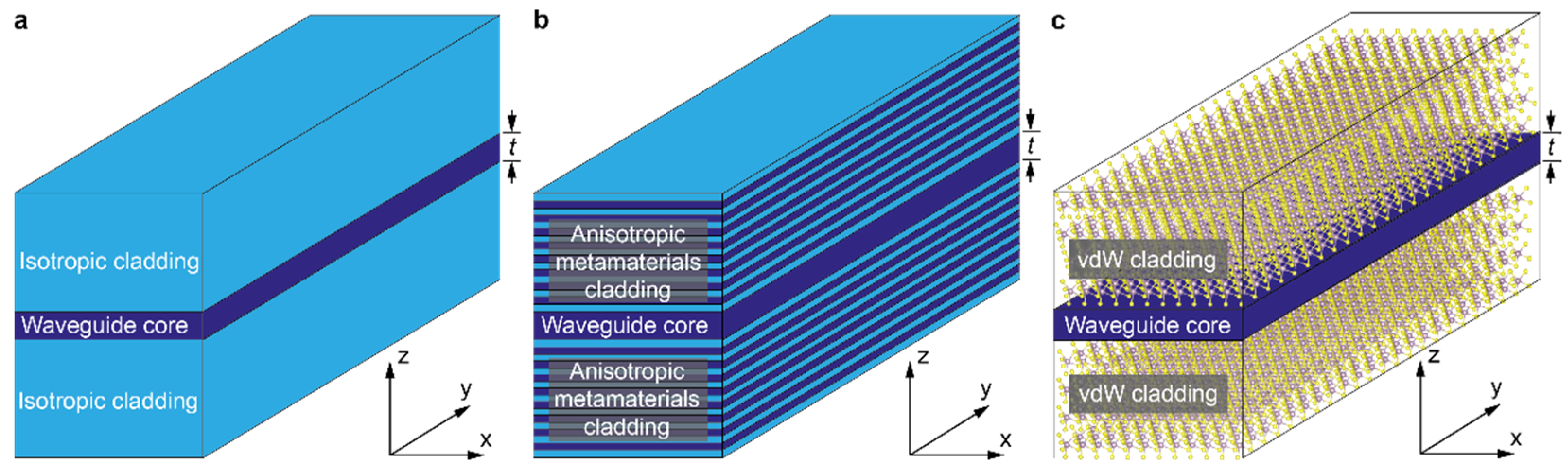
Abstract
:1. Introduction
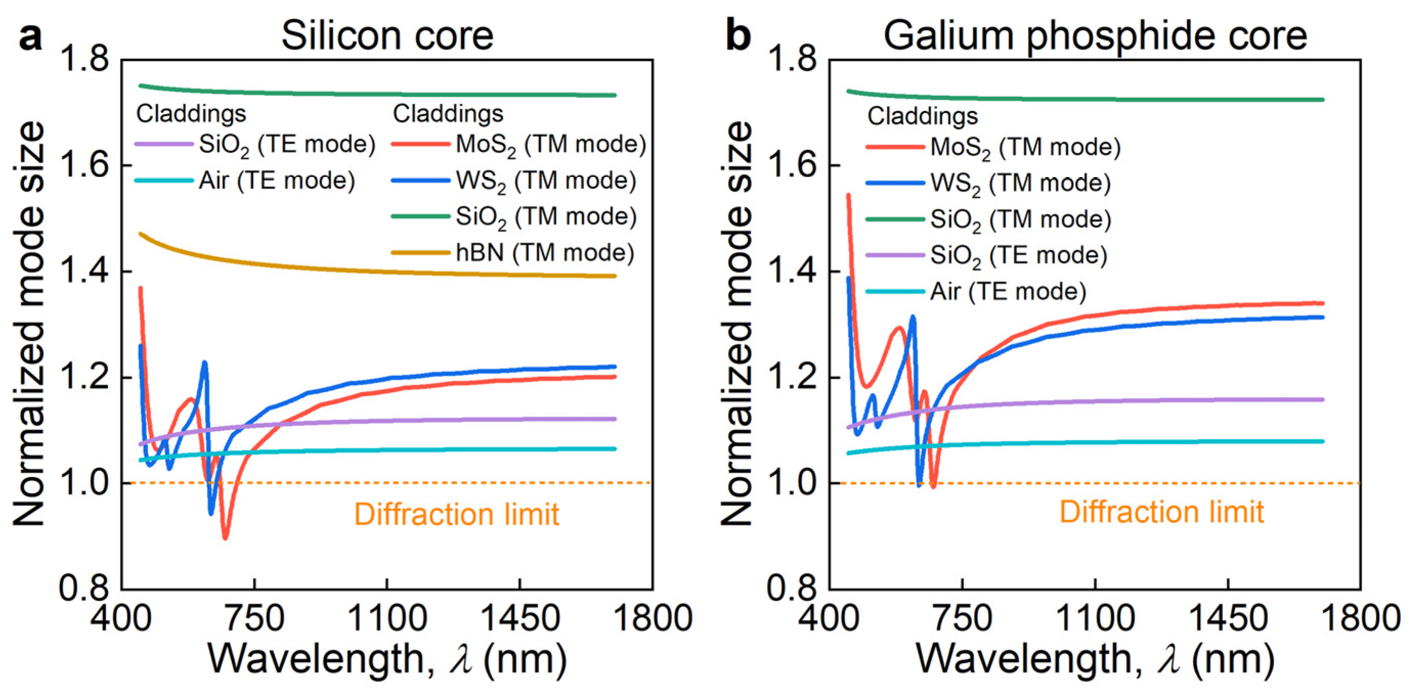
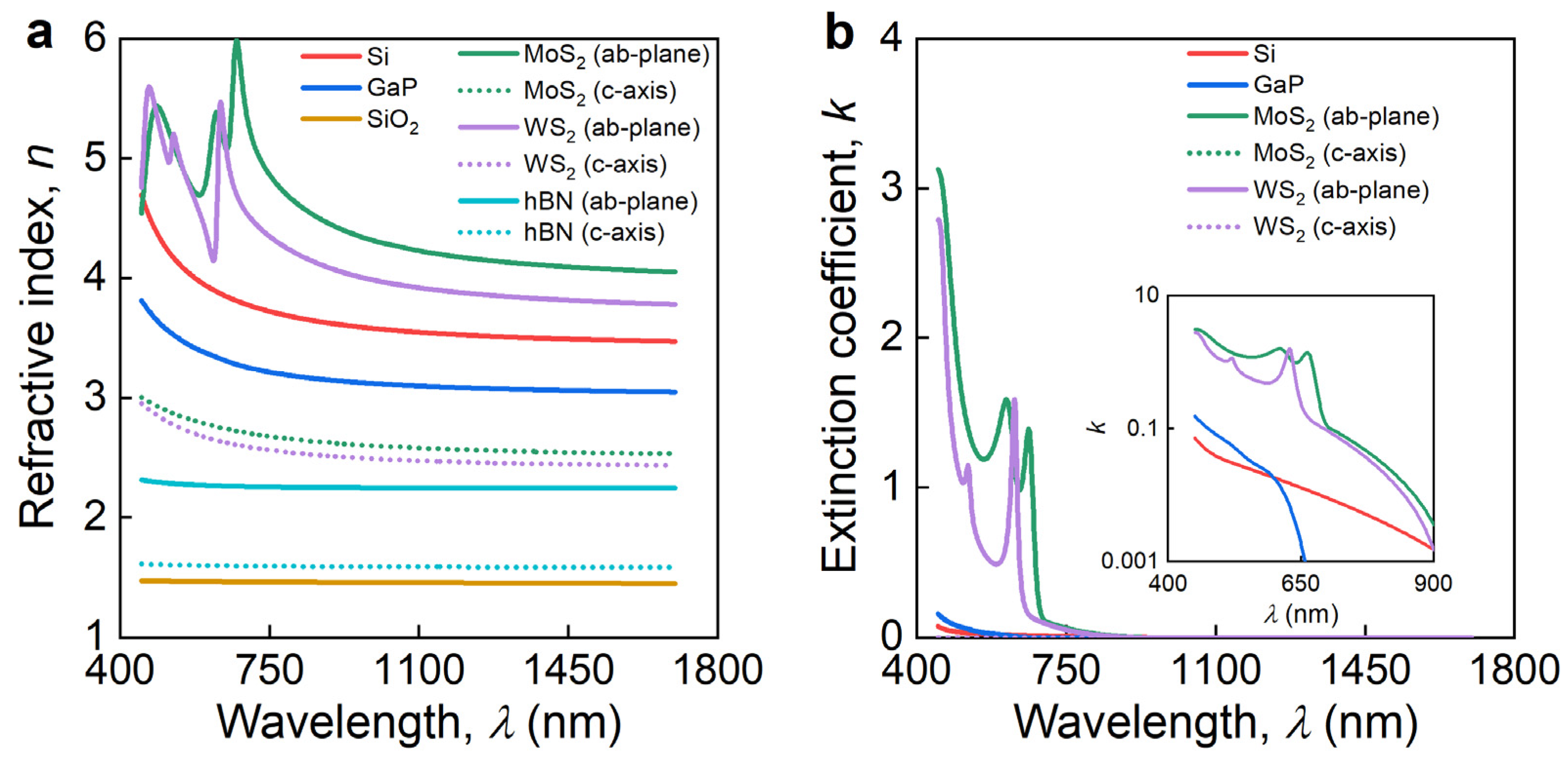
2. Results
3. Discussion
Author Contributions
Funding
Institutional Review Board Statement
Informed Consent Statement
Data Availability Statement
Conflicts of Interest
Appendix A

References
- Jahani, S.; Jacob, Z. Transparent Subdiffraction Optics: Nanoscale Light Confinement without Metal. Optica 2014, 1, 96. [Google Scholar] [CrossRef]
- Jahani, S.; Kim, S.; Atkinson, J.; Wirth, J.C.; Kalhor, F.; Noman, A.A.; Newman, W.D.; Shekhar, P.; Han, K.; Van, V.; et al. Controlling Evanescent Waves Using Silicon Photonic All-Dielectric Metamaterials for Dense Integration. Nat. Commun. 2018, 9, 1893. [Google Scholar] [CrossRef] [Green Version]
- Mia, M.B.; Ahmed, S.Z.; Ahmed, I.; Lee, Y.J.; Qi, M.; Kim, S. Exceptional Coupling in Photonic Anisotropic Metamaterials for Extremely Low Waveguide Crosstalk. Optica 2020, 7, 881. [Google Scholar] [CrossRef]
- van Niekerk, M.; Jahani, S.; Bickford, J.; Cho, P.; Anderson, S.; Leake, G.; Coleman, D.; Fanto, M.L.; Tison, C.C.; Howland, G.A.; et al. Two-Dimensional Extreme Skin Depth Engineering for CMOS Photonics. J. Opt. Soc. Am. B 2021, 38, 1307. [Google Scholar] [CrossRef]
- Jahani, S.; Jacob, Z. All-Dielectric Metamaterials. Nat. Nanotechnol. 2016, 11, 23–36. [Google Scholar] [CrossRef] [PubMed]
- Ermolaev, G.A.; Grudinin, D.V.; Stebunov, Y.V.; Voronin, K.V.; Kravets, V.G.; Duan, J.; Mazitov, A.B.; Tselikov, G.I.; Bylinkin, A.; Yakubovsky, D.I.; et al. Giant Optical Anisotropy in Transition Metal Dichalcogenides for Next-Generation Photonics. Nat. Commun. 2021, 12, 854. [Google Scholar] [CrossRef]
- Bozhevolnyi, S.I.; Volkov, V.S.; Devaux, E.; Laluet, J.-Y.; Ebbesen, T.W. Channel Plasmon Subwavelength Waveguide Components Including Interferometers and Ring Resonators. Nature 2006, 440, 508–511. [Google Scholar] [CrossRef] [PubMed]
- Fedyanin, D.Y.; Yakubovsky, D.I.; Kirtaev, R.V.; Volkov, V.S. Ultralow-Loss CMOS Copper Plasmonic Waveguides. Nano Lett. 2016, 16, 362–366. [Google Scholar] [CrossRef]
- Thomaschewski, M.; Zenin, V.A.; Fiedler, S.; Wolff, C.; Bozhevolnyi, S.I. Plasmonic Lithium Niobate Mach–Zehnder Modulators. Nano Lett. 2022, 22, 6471–6475. [Google Scholar] [CrossRef]
- Minin, I.V.; Minin, O.V.; Glinskiy, I.A.; Khabibullin, R.A.; Malureanu, R.; Lavrinenko, A.; Yakubovsky, D.I.; Volkov, V.S.; Ponomarev, D.S. Experimental Verification of a Plasmonic Hook in a Dielectric Janus Particle. Appl. Phys. Lett. 2021, 118, 131107. [Google Scholar] [CrossRef]
- Hsu, C.W.; Zhen, B.; Lee, J.; Chua, S.-L.; Johnson, S.G.; Joannopoulos, J.D.; Soljačić, M. Observation of Trapped Light within the Radiation Continuum. Nature 2013, 499, 188–191. [Google Scholar] [CrossRef] [PubMed] [Green Version]
- Mekis, A.; Chen, J.C.; Kurland, I.; Fan, S.; Villeneuve, P.R.; Joannopoulos, J.D. High Transmission through Sharp Bends in Photonic Crystal Waveguides. Phys. Rev. Lett. 1996, 77, 3787–3790. [Google Scholar] [CrossRef] [PubMed]
- Dai, D.; Shi, Y.; He, S. Comparative Study of the Integration Density for Passive Linear Planar Light-Wave Circuits Based on Three Different Kinds of Nanophotonic Waveguide. Appl. Opt. 2007, 46, 1126. [Google Scholar] [CrossRef] [PubMed]
- Lebsir, Y.; Boroviks, S.; Thomaschewski, M.; Bozhevolnyi, S.I.; Zenin, V.A. Ultimate Limit for Optical Losses in Gold, Revealed by Quantitative Near-Field Microscopy. Nano Lett. 2022, 22, 5759–5764. [Google Scholar] [CrossRef] [PubMed]
- Hemmati, H.; Magnusson, R. Applicability of Rytov’s Full Effective-Medium Formalism to the Physical Description and Design of Resonant Metasurfaces. ACS Photonics 2020, 7, 3177–3187. [Google Scholar] [CrossRef]
- Rytov, S.M. Electromagnetic Properties of a Finely Stratified Medium. Sov. Phys. JETP 1956, 2, 446–475. [Google Scholar]
- Kats, M.A.; Genevet, P.; Aoust, G.; Yu, N.; Blanchard, R.; Aieta, F.; Gaburro, Z.; Capasso, F. Giant Birefringence in Optical Antenna Arrays with Widely Tailorable Optical Anisotropy. Proc. Natl. Acad. Sci. USA 2012, 109, 12364–12368. [Google Scholar] [CrossRef] [Green Version]
- Niu, S.; Joe, G.; Zhao, H.; Zhou, Y.; Orvis, T.; Huyan, H.; Salman, J.; Mahalingam, K.; Urwin, B.; Wu, J.; et al. Giant Optical Anisotropy in a Quasi-One-Dimensional Crystal. Nat. Photonics 2018, 12, 392–396. [Google Scholar] [CrossRef]
- Verre, R.; Baranov, D.G.; Munkhbat, B.; Cuadra, J.; Käll, M.; Shegai, T. Transition Metal Dichalcogenide Nanodisks as High-Index Dielectric Mie Nanoresonators. Nat. Nanotechnol. 2019, 14, 679–684. [Google Scholar] [CrossRef] [Green Version]
- Ermolaev, G.; Voronin, K.; Baranov, D.G.; Kravets, V.; Tselikov, G.; Stebunov, Y.; Yakubovsky, D.; Novikov, S.; Vyshnevyy, A.; Mazitov, A.; et al. Topological Phase Singularities in Atomically Thin High-Refractive-Index Materials. Nat. Commun. 2022, 13, 2049. [Google Scholar] [CrossRef]
- Ermolaev, G.A.; Stebunov, Y.V.; Vyshnevyy, A.A.; Tatarkin, D.E.; Yakubovsky, D.I.; Novikov, S.M.; Baranov, D.G.; Shegai, T.; Nikitin, A.Y.; Arsenin, A.V.; et al. Broadband Optical Properties of Monolayer and Bulk MoS2. npj 2D Mater. Appl. 2020, 4, 21. [Google Scholar] [CrossRef]
- Mounet, N.; Gibertini, M.; Schwaller, P.; Campi, D.; Merkys, A.; Marrazzo, A.; Sohier, T.; Castelli, I.E.; Cepellotti, A.; Pizzi, G.; et al. Two-Dimensional Materials from High-Throughput Computational Exfoliation of Experimentally Known Compounds. Nat. Nanotechnol. 2018, 13, 246–252. [Google Scholar] [CrossRef] [PubMed] [Green Version]
- Munkhbat, B.; Yankovich, A.B.; Baranov, D.G.; Verre, R.; Olsson, E.; Shegai, T.O. Transition Metal Dichalcogenide Metamaterials with Atomic Precision. Nat. Commun. 2020, 11, 4604. [Google Scholar] [CrossRef] [PubMed]
- Munkhbat, B.; Küçüköz, B.; Baranov, D.G.; Antosiewicz, T.J.; Shegai, T.O. Nanostructured Transition Metal Dichalcogenide Multilayers for Advanced Nanophotonics. arXiv 2022, arXiv:2202.04898. [Google Scholar]
- Tselikov, G.I.; Ermolaev, G.A.; Popov, A.A.; Tikhonowski, G.V.; Panova, D.A.; Taradin, A.S.; Vyshnevyy, A.A.; Syuy, A.V.; Klimentov, S.M.; Novikov, S.M.; et al. Transition Metal Dichalcogenide Nanospheres for High-Refractive-Index Nanophotonics and Biomedical Theranostics. Proc. Natl. Acad. Sci. USA 2022, 119, e2208830119. [Google Scholar] [CrossRef]
- Okamoto, K. Fundamentals of Optical Waveguides, 2nd ed.; Optics and Photonics Series; Elsevier: Amsterdam, The Netherlands, 2005; ISBN 0125250967. [Google Scholar]
- Oulton, R.F.; Bartal, G.; Pile, D.F.P.; Zhang, X. Confinement and Propagation Characteristics of Subwavelength Plasmonic Modes. New J. Phys. 2008, 10, 105018. [Google Scholar] [CrossRef]
- Khmelevskaia, D.; Markina, D.I.; Fedorov, V.V.; Ermolaev, G.A.; Arsenin, A.V.; Volkov, V.S.; Goltaev, A.S.; Zadiranov, Y.M.; Tzibizov, I.A.; Pushkarev, A.P.; et al. Directly Grown Crystalline Gallium Phosphide on Sapphire for Nonlinear All-Dielectric Nanophotonics. Appl. Phys. Lett. 2021, 118, 201101. [Google Scholar] [CrossRef]
- Novoselov, K.S.; Mishchenko, A.; Carvalho, A.; Castro Neto, A.H. 2D Materials and van Der Waals Heterostructures. Science 2016, 353, aac9439. [Google Scholar] [CrossRef] [Green Version]
- Taboada-Gutiérrez, J.; Álvarez-Pérez, G.; Duan, J.; Ma, W.; Crowley, K.; Prieto, I.; Bylinkin, A.; Autore, M.; Volkova, H.; Kimura, K.; et al. Broad Spectral Tuning of Ultra-Low-Loss Polaritons in a van Der Waals Crystal by Intercalation. Nat. Mater. 2020, 19, 964–968. [Google Scholar] [CrossRef]
- Duan, J.; Capote-Robayna, N.; Taboada-Gutiérrez, J.; Álvarez-Pérez, G.; Prieto, I.; Martín-Sánchez, J.; Nikitin, A.Y.; Alonso-González, P. Twisted Nano-Optics: Manipulating Light at the Nanoscale with Twisted Phonon Polaritonic Slabs. Nano Lett. 2020, 20, 5323–5329. [Google Scholar] [CrossRef]


Publisher’s Note: MDPI stays neutral with regard to jurisdictional claims in published maps and institutional affiliations. |
© 2022 by the authors. Licensee MDPI, Basel, Switzerland. This article is an open access article distributed under the terms and conditions of the Creative Commons Attribution (CC BY) license (https://creativecommons.org/licenses/by/4.0/).
Share and Cite
Ermolaev, G.; Grudinin, D.; Voronin, K.; Vyshnevyy, A.; Arsenin, A.; Volkov, V. Van Der Waals Materials for Subdiffractional Light Guidance. Photonics 2022, 9, 744. https://doi.org/10.3390/photonics9100744
Ermolaev G, Grudinin D, Voronin K, Vyshnevyy A, Arsenin A, Volkov V. Van Der Waals Materials for Subdiffractional Light Guidance. Photonics. 2022; 9(10):744. https://doi.org/10.3390/photonics9100744
Chicago/Turabian StyleErmolaev, Georgy, Dmitriy Grudinin, Kirill Voronin, Andrey Vyshnevyy, Aleksey Arsenin, and Valentyn Volkov. 2022. "Van Der Waals Materials for Subdiffractional Light Guidance" Photonics 9, no. 10: 744. https://doi.org/10.3390/photonics9100744