Design and Simulation of Terahertz Perfect Absorber with Tunable Absorption Characteristic Using Fractal-Shaped Graphene Layers

Abstract
:1. Introduction
2. Theory and Background
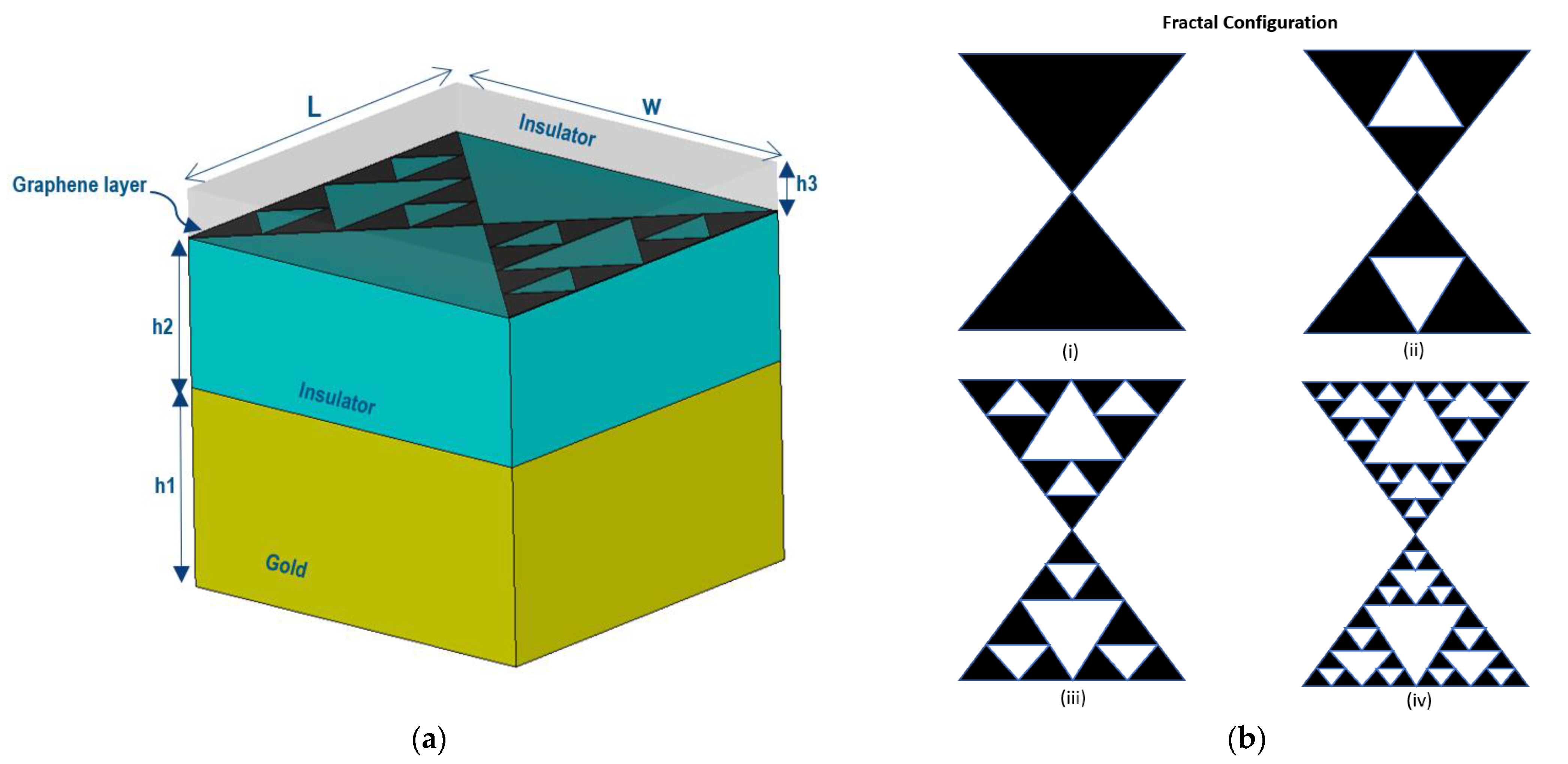
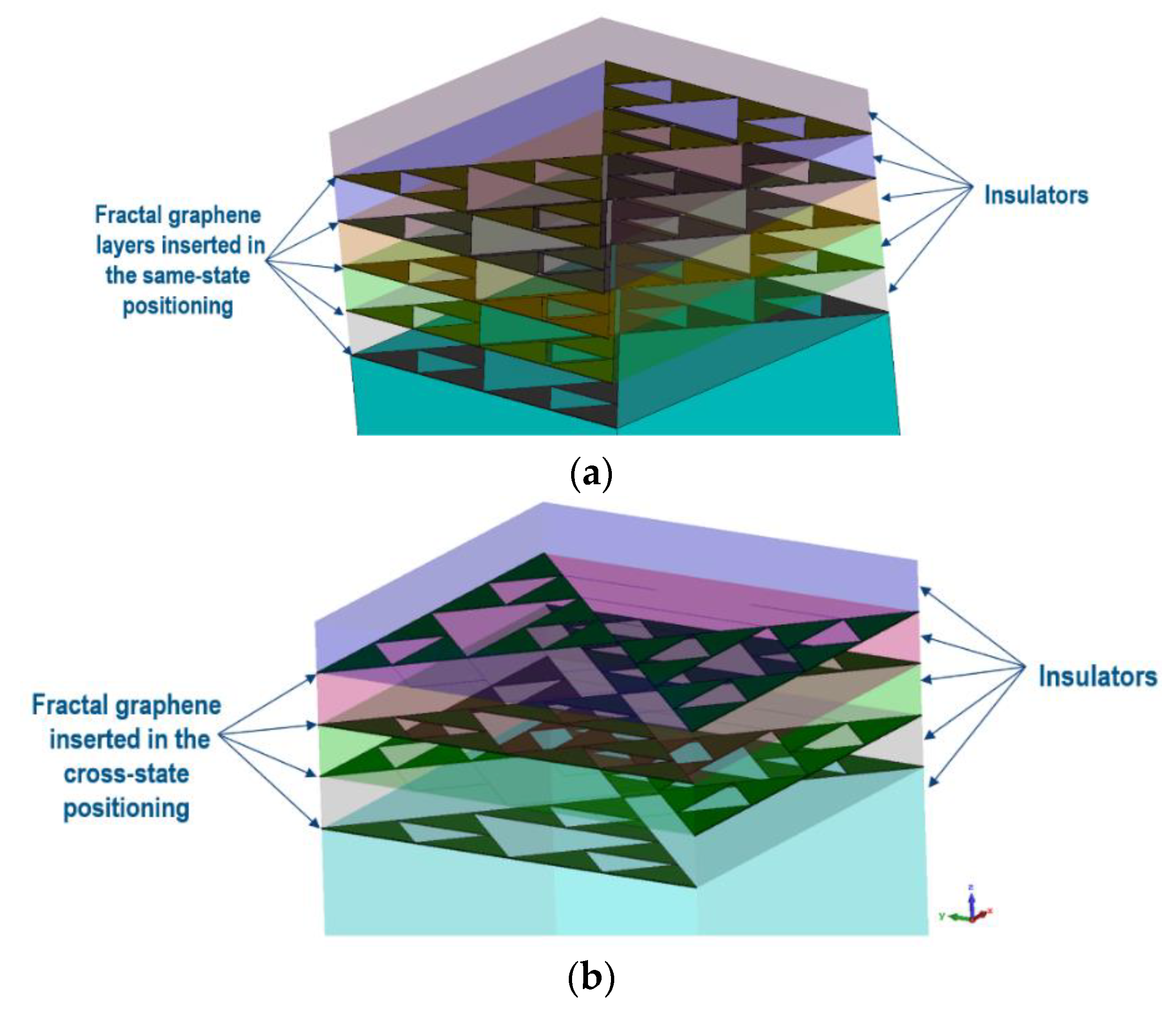
3. Structural Geometry
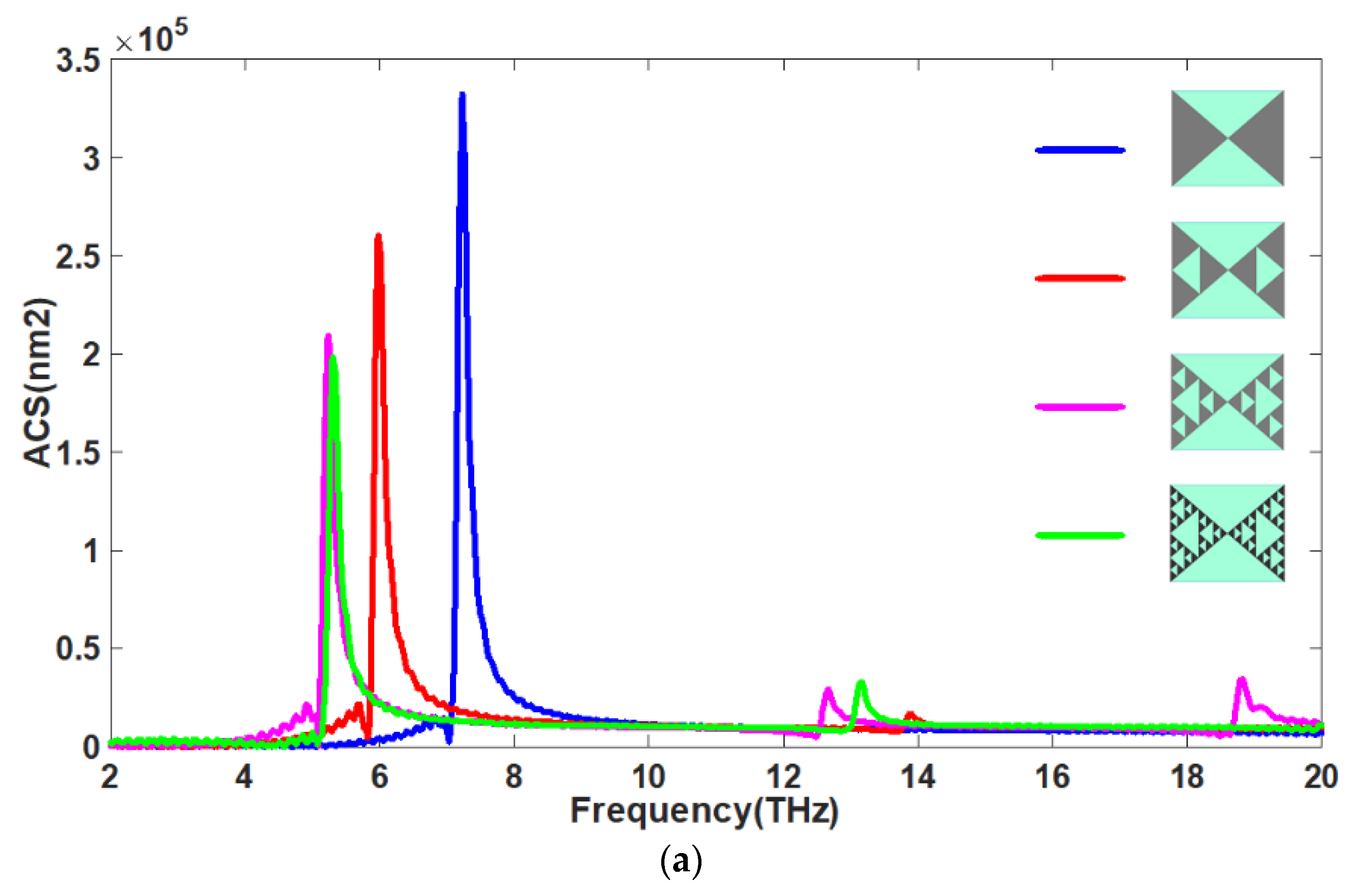
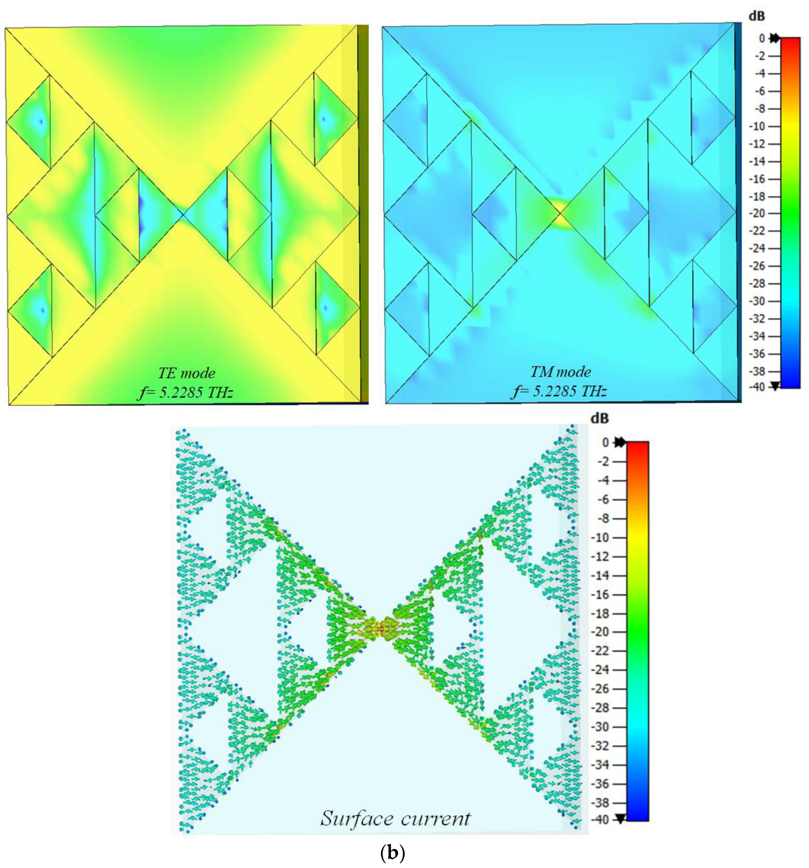
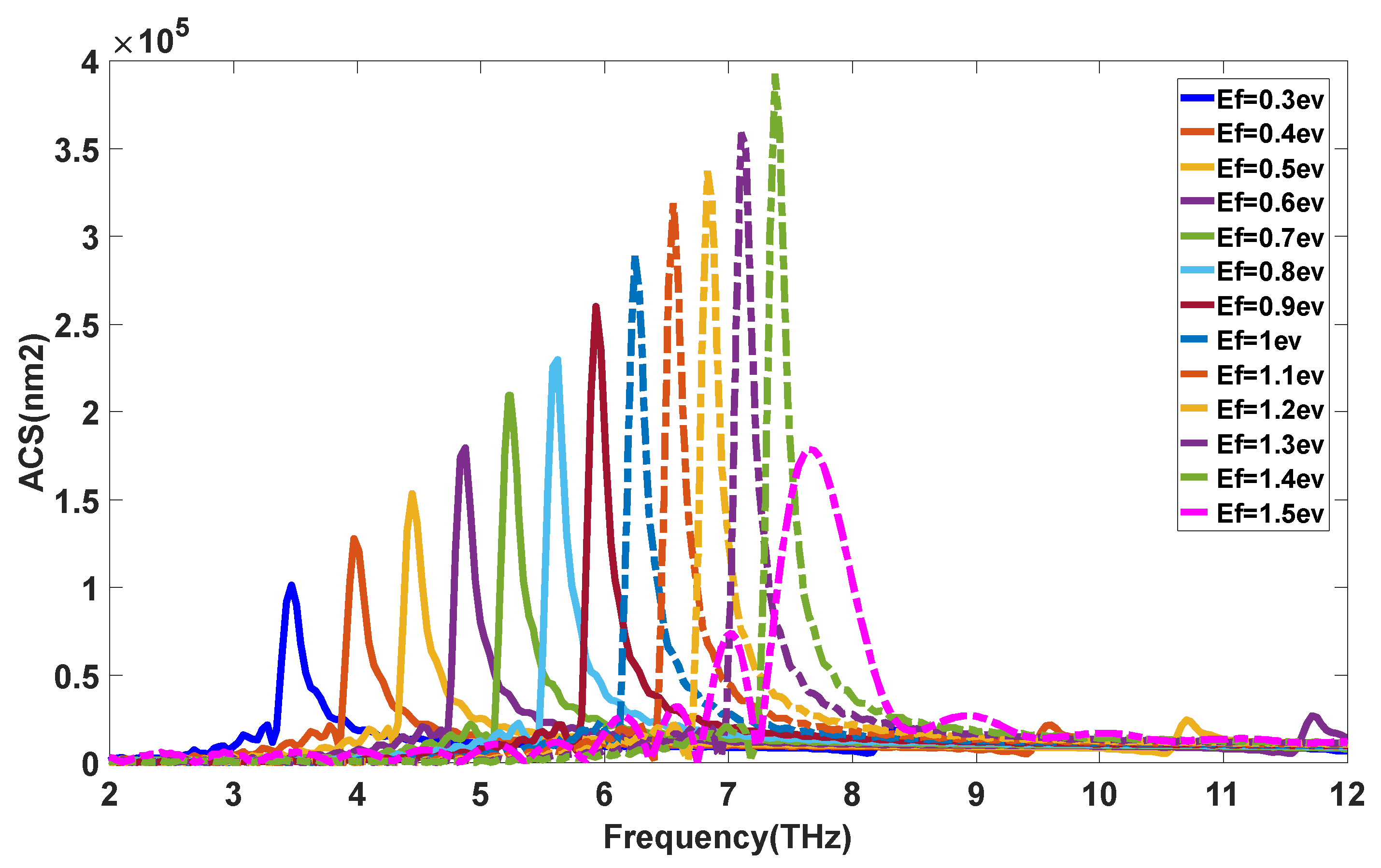
4. Simulation and Discussion
5. Conclusions
Author Contributions
Funding
Institutional Review Board Statement
Informed Consent Statement
Data Availability Statement
Conflicts of Interest
References
- Shen, G.; Zhang, M.; Ji, Y.; Huang, W.; Yu, H.; Shi, J. Broadband terahertz metamaterial absorber based on simple multi-ring structures. AIP Adv. 2018, 8, 075206. [Google Scholar] [CrossRef] [Green Version]
- Carranza, I.E.; Grant, J.P.; Gough, J.; Cumming, D. Terahertz metamaterial absorbers implemented in CMOS technology for imaging applications: Scaling to large format focal plane arrays. IEEE J. Sel. Top. Quantum Electron. 2017, 23, 1–8. [Google Scholar] [CrossRef] [Green Version]
- Zhong, S. Progress in terahertz nondestructive testing: A review. Front. Mech. Eng. 2019, 14, 273–281. [Google Scholar] [CrossRef]
- Lewis, R.A. A review of terahertz detectors. J. Phys. D Appl. Phys. 2019, 52, 433001. [Google Scholar] [CrossRef]
- Haxha, S.; AbdelMalek, F.; Ouerghi, F.; Charlton, M.D.B.; Aggoun, A.; Fang, X. Metamaterial superlenses operating at visible wavelength for imaging applications. Sci. Rep. 2018, 8, 16119. [Google Scholar] [CrossRef] [Green Version]
- Asl, A.B.; Rostami, A.; Amiri, I.S. Terahertz band pass filter design using multilayer metamaterials. Opt. Quantum Electron. 2020, 52, 155. [Google Scholar] [CrossRef]
- Ghosh, S.K.; Yadav, V.S.; Das, S.; Bhattacharyya, S. Tunable graphene-based metasurface for polarization-independent broadband absorption in Lower Mid-Infrared (MIR) range. IEEE Trans. Electromagn. Compat. 2020, 62, 346–354. [Google Scholar] [CrossRef]
- Cui, Z.; Zhu, D.; Yue, L.; Hu, H.; Chen, S.; Wang, X.; Wang, Y. Development of frequency-tunable multiple-band terahertz absorber based on control of polarization angles. Opt. Express 2019, 27, 22190–22197. [Google Scholar] [CrossRef]
- Cai, Y.; Li, S.; Zhou, Y.; Wang, X.; Xu, K.-D.; Guo, R.; Joines, W.T. Tunable and anisotropic dual-band metamaterial absorber using elliptical graphene-black phosphorus pairs. Nanoscale Res. Lett. 2019, 14, 346. [Google Scholar] [CrossRef] [Green Version]
- Li, H.; Ji, C.; Ren, Y.; Hu, J.; Qin, M.; Wang, L. Investigation of multiband plasmonic metamaterial perfect absorbers based on graphene ribbons by the phase-coupled method. Carbon 2019, 141, 481–487. [Google Scholar] [CrossRef]
- Venkatachalam, S.; Zeranska-Chudek, K.; Zdrojek, M.; Hourlier, D. Carbon-based terahertz absorbers: Materials, applications, and perspectives. Nano Sel. 2020, 1, 471–490. [Google Scholar] [CrossRef]
- Yi, Z.; Liang, C.; Chen, X.; Zhou, Z.; Tang, Y.; Ye, X.; Yi, Y.; Wang, J.; Wu, P. Dual-band plasmonic perfect absorber based on graphene metamaterials for refractive index sensing application. Micromachines 2019, 10, 443. [Google Scholar] [CrossRef] [PubMed] [Green Version]
- Huang, H.; Xia, H.; Xie, W.; Guo, Z.; Li, H.; Xie, D. Design of broadband graphene-metamaterial absorbers for permittivity sensing at mid-infrared regions. Sci. Rep. 2018, 8, 4183. [Google Scholar] [CrossRef] [PubMed] [Green Version]
- Seren, H.R.; Keiser, G.R.; Cao, L.; Zhang, J.; Strikwerda, A.C.; Fan, K.; Metcalfe, G.D.; Wraback, M.; Zhang, X.; Averitt, R.D. Optically modulated multiband terahertz perfect absorber. Adv. Opt. Mater. 2014, 2, 1221–1226. [Google Scholar] [CrossRef]
- Cheng, X.; Huang, R.; Xu, J.; Xu, X. Broadband terahertz near-perfect absorbers. ACS Appl. Mater. Interfaces 2020, 12, 33352–33360. [Google Scholar] [CrossRef] [PubMed]
- Hossain, M.J.; Faruque, M.R.I.; Islam, M.T. Perfect metamaterial absorber with high fractional bandwidth for solar energy harvesting. PLoS ONE 2018, 13, e0207314. [Google Scholar] [CrossRef] [Green Version]
- Mulla, B.; Sabah, C. Perfect metamaterial absorber design for solar cell applications. Waves Random Complex Media 2015, 25, 382–392. [Google Scholar] [CrossRef]
- Wang, Y.; Sun, T.; Paudel, T.; Zhang, Y.; Ren, Z.; Kempa, K. Metamaterial-plasmonic absorber structure for high efficiency amorphous silicon solar cells. Nano Lett. 2012, 12, 440–445. [Google Scholar] [CrossRef]
- Wallace, G.Q.; Lagugné-Labarthet, F. Advancements in fractal plasmonics: Structures, optical properties, and applications. Analyst 2019, 144, 13–30. [Google Scholar] [CrossRef]
- Ullah, Z.; Witjaksono, G.; Nawi, I.; Tansu, N.; Irfan Khattak, M.; Junaid, M. A review on the development of tunable graphene nanoantennas for terahertz optoelectronic and plasmonic applications. Sensors 2020, 20, 1401. [Google Scholar] [CrossRef] [Green Version]
- Guo, C.; Zhang, J.; Xu, W.; Liu, K.; Yuan, X.; Qin, S.; Zhu, Z. Graphene-based perfect absorption structures in the visible to terahertz band and their optoelectronics applications. Nanomaterials 2018, 8, 1033. [Google Scholar] [CrossRef] [Green Version]
- Qi, Y.; Zhang, Y.; Liu, C.; Zhang, T.; Zhang, B.; Wang, L.; Deng, X.; Wang, X.; Yu, Y. A tunable terahertz metamaterial absorber composed of hourglass-shaped graphene arrays. Nanomaterials 2020, 10, 533. [Google Scholar] [CrossRef] [PubMed] [Green Version]
- Mishra, R.; Panwar, R. Investigation of graphene fractal frequency selective surface loaded terahertz absorber. Opt. Quantum Electron. 2020, 52, 317. [Google Scholar] [CrossRef]
- Nourbakhsh, M.; Zareian-Jahromi, E.; Basiri, R. Ultra-wideband terahertz metamaterial absorber based on Snowflake Koch Fractal dielectric loaded graphene. Opt. Express 2019, 27, 32958–32969. [Google Scholar] [CrossRef]
- Bao, Z.; Tang, Y.; Hu, Z.-D.; Zhang, C.; Balmakou, A.; Khakhomov, S.; Semchenko, I.; Wang, J. Inversion method characterization of graphene-based coordination absorbers incorporating periodically patterned metal ring metasurfaces. Nanomaterials 2020, 10, 1102. [Google Scholar] [CrossRef] [PubMed]
- Shen, H.; Liu, F.; Liu, C.; Zeng, D.; Guo, B.; Wei, Z.; Wang, F.; Tan, C.; Huang, X.; Meng, H. A Polarization-insensitive and wide-angle terahertz absorber with ring-porous patterned Graphene METASURFACE. Nanomaterials 2020, 10, 1410. [Google Scholar] [CrossRef] [PubMed]
- Zhu, H.; Zhang, Y.; Ye, L.; Li, Y.; Xu, Y.; Xu, R. Switchable and tunable terahertz metamaterial absorber with broadband and multi-band absorption. Opt. Express 2020, 28, 38626–38637. [Google Scholar] [CrossRef]
- Cai, Y.; Guo, Y.; Zhou, Y.; Huang, X.; Yang, G.; Zhu, J. Tunable dual-band terahertz absorber with all-dielectric configuration based on graphene. Opt. Express 2020, 28, 31524–31534. [Google Scholar] [CrossRef] [PubMed]
- Xu, K.-D.; Li, J.; Zhang, A.; Chen, Q. Tunable multi-band terahertz absorber using a single-layer square graphene ring structure with T-shaped graphene strips. Opt. Express 2020, 28, 11482–11492. [Google Scholar] [CrossRef]
- Xu, K.-D.; Cai, Y.; Cao, X.; Guo, Y.; Zhang, Y.; Chen, Q. Multiband terahertz absorbers using T-shaped slot-patterned graphene and its complementary structure. J. Opt. Soc. Am. B 2020, 37, 3034–3040. [Google Scholar] [CrossRef]
- Xie, T.; Chen, D.; Yang, H.; Xu, Y.; Zhang, Z.; Yang, J. Tunable broadband terahertz waveband absorbers based on fractal technology of graphene metamaterial. Nanomaterials 2021, 11, 269. [Google Scholar] [CrossRef]
- Zubair, A.; Zubair, M.; Danner, A.; Mehmood, M.Q. Engineering multimodal spectrum of Cayley tree fractal meta-resonator supercells for ultrabroadband terahertz light absorption. Nanophotonics 2020, 9, 633–644. [Google Scholar] [CrossRef]
- Zubair, A.; Mehmood, M.Q.; Zubair, M. Design of a fractal metasurface based terahertz broadband absorber. In 2019 PhotonIcs & Electromagnetics Research Symposium-Spring (PIERS-Spring); IEEE: Piscataway Township, NJ, USA, 2019; pp. 663–666. [Google Scholar]
- Kenney, M.; Grant, J.; Shah, Y.D.; Escorcia-Carranza, I.; Humphreys, M.; Cumming, D.R.S. Octave-spanning broadband absorption of terahertz light using metasurface fractal-cross absorbers. ACS Photonics 2017, 4, 2604–2612. [Google Scholar] [CrossRef]
- Arik, K.; Abdollahramezani, S.; Farajollahi, S.; Khavasi, A.; Rejaei, B. Design of mid-infrared ultra-wideband metallic absorber based on circuit theory. Opt. Commun. 2016, 381, 309–313. [Google Scholar] [CrossRef]
- Andryieuski, A.; Lavrinenko, A.V. Graphene metamaterials based tunable terahertz absorber: Effective surface conductivity approach. Opt. Express 2013, 21, 9144–9155. [Google Scholar] [CrossRef] [PubMed] [Green Version]
- Zhang, Y.; Li, T.; Chen, Q.; Zhang, H.; O’Hara, J.F.; Abele, E.; Taylor, A.J.; Chen, H.-T.; Azad, A.K. Independently tunable dual-band perfect absorber based on graphene at mid-infrared frequencies. Sci. Rep. 2015, 5, 18463. [Google Scholar] [CrossRef] [Green Version]
- Piper, J.R.; Fan, S. Total absorption in a graphene monolayer in the optical regime by critical coupling with a photonic crystal guided resonance. ACS Photonics 2014, 1, 347–353. [Google Scholar] [CrossRef]
- Bohren, C.F.; Huffman, D.R. Absorption and Scattering of Light by Small Particles; John Wiley & Sons: Hoboken, NJ, USA, 2008. [Google Scholar]
- Alaee, R. Optical Nanoantennas and Their Use as Perfect Absorbers; Karlsruher Institut für Technologie: Karlsruhe, Germany, 2015. [Google Scholar]
- Alaee, R.; Albooyeh, M.; Rockstuhl, C. Theory of metasurface based perfect absorbers. J. Phys. D Appl. Phys. 2017, 50, 503002. [Google Scholar] [CrossRef] [Green Version]
- Jabbarzadeh, F.; Heydari, M.; Habibzadeh-Sharif, A. A comparative analysis of the accuracy of Kubo formulations for graphene plasmonics. Mater. Res. Express 2019, 6, 086209. [Google Scholar] [CrossRef]
- Linden, S.; Enkrich, C.; Dolling, G.; Klein, M.W.; Zhou, J.; Koschny, T.; Soukoulis, C.M.; Burger, S.; Schmidt, F.; Wegener, M. Photonic metamaterials: Magnetism at optical frequencies. IEEE J. Sel. Top. Quantum Electron. 2006, 12, 1097–1105. [Google Scholar] [CrossRef] [Green Version]
- Xiao, B.; Gu, M.; Xiao, S. Broadband, wide-angle and tunable terahertz absorber based on cross-shaped graphene arrays. Appl. Opt. 2017, 56, 5458–5462. [Google Scholar] [CrossRef] [PubMed]
- Arik, K.; AbdollahRamezani, S.; Khavasi, A. Polarization insensitive and broadband terahertz absorber using graphene disks. Plasmonics 2017, 12, 393–398. [Google Scholar] [CrossRef]
- Xu, Z.; Wu, D.; Liu, Y.; Liu, C.; Yu, Z.; Yu, L.; Ye, H. Design of a tunable ultra-broadband terahertz absorber based on multiple layers of graphene ribbons. Nanoscale Res. Lett. 2018, 13, 143. [Google Scholar] [CrossRef] [PubMed] [Green Version]
- Bott, A.W. Electrochemistry of semiconductors. Curr. Sep. 1998, 17, 87–92. [Google Scholar]
- Stoliar, P.; Calò, A.; Valle, F.; Biscarini, F. Fabrication of fractal surfaces by electron beam lithography. IEEE Trans. Nanotechnol. 2010, 9, 229–236. [Google Scholar] [CrossRef]


| h1 | h2 | h3 | L | W |
|---|---|---|---|---|
| 3 μm | 1.5 μm | 50 nm | 0.4 μm | 0.4 μm |
| Fermi Potential (eV) | 0.3 | 0.4 | 0.5 | 0.6 | 0.7 | 0.8 | 0.9 | 1 | 1.1 | 1.2 |
|---|---|---|---|---|---|---|---|---|---|---|
| Plasmonic resonant frequency (THz) | 3.47 | 3.978 | 4.447 | 4.8768 | 5.2285 | 5.6192 | 5.932 | 6.2445 | 6.5571 | 6.8307 |
| Amplitude of absorption peak (×105 nm2) | 1.011 | 1.2775 | 1.529 | 1.7922 | 2.0892 | 2.2945 | 2.5998 | 2.898 | 3.186 | 3.3675 |
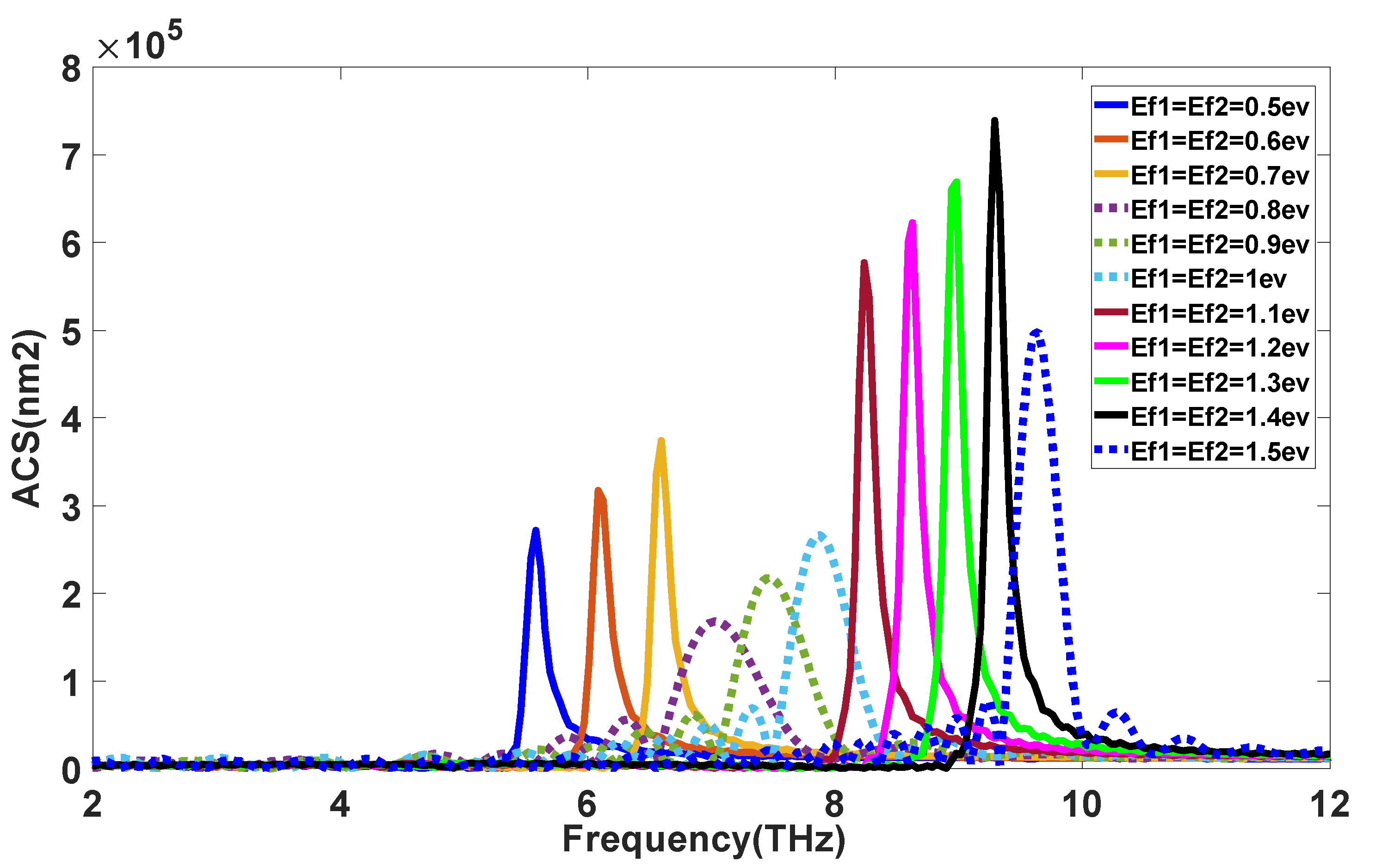
| Absorbers with Double Fractal Graphene Layers | Plasmonic Frequency (THz) | The Amplitude of Absorption Peak (×105 nm2) |
|---|---|---|
| In the same-state positioning | 6.5962 | 3.7326 |
| In the cross-state positioning | 16.285 4.52 | 1.87564 0.66911 |
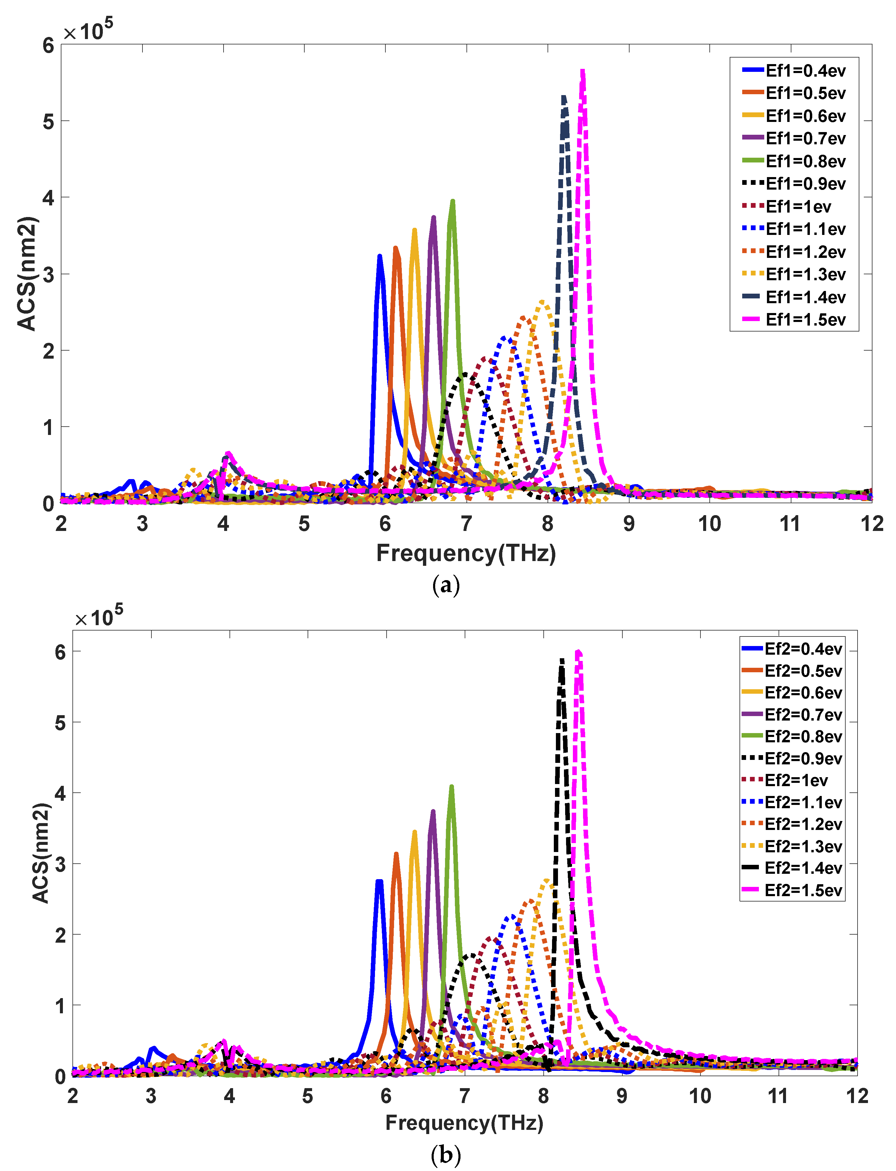
| Fermi Potential (eV) | 0.4 | 0.5 | 0.6 | 0.7 | 0.8 | 0.9 | 1 | 1.1 | 1.2 |
|---|---|---|---|---|---|---|---|---|---|
| Plasmonic Frequency (THz) | 5.9319 | 6.12725 | 6.36172 | 6.5962 | 6.83066 | 6.987 | 7.26052 | 7.495 | 7.7295 |
| The Amplitude of Absorption Peak (×105 nm2) | 3.2249 | 3.13688 | 3.57054 | 3.7326 | 3.94542 | 1.63982 | 1.8853 | 2.16426 | 2.42533 |
| Beamwidth of Absorption Response (GHz)| (Approximately) | 120 | 120.1 | 123.9 | 116.2 | 116 | 540.3 | 482.2 | 427.8 | 397.3 |
| Fermi Potential (eV) | 0.4 | 0.5 | 0.6 | 0.7 | 0.8 | 0.9 | 1 | 1.1 | 1.2 |
|---|---|---|---|---|---|---|---|---|---|
| Plasmonic Frequency (THz) | 5.893 | 6.1237 | 6.3617 | 6.5962 | 6.8307 | 7.0651 | 7.3387 | 7.5731 | 7.8076 |
| The Amplitude of Absorption Peak (×105 nm2) | 2.74937 | 3.33415 | 3.44014 | 3.7326 | 4.08488 | 1.70679 | 1.94734 | 2.25912 | 2.47892 |
| Beamwidth of Absorption Response (GHz) (Approximately) | 125 | 118.85 | 116.1 | 116.2 | 114.9 | 542.98 | 498.5 | 440 | 415.93 |
| Fermi Potential (eV) | 0.5 | 0.6 | 0.7 | 0.8 | 0.9 | 1 | 1.1 | 1.2 | 1.3 |
|---|---|---|---|---|---|---|---|---|---|
| Plasmonic Frequency (THz) | 5.5802 | 6.0882 | 6.5962 | 7.0261 | 7.4559 | 7.8858 | 8.2375 | 8.6283 | 8.98 |
| The Amplitude of Absorption Peak (×105 nm2) | 2.70932 | 3.16794 | 3.7326 | 1.67307 | 2.16996 | 2.65677 | 5.76659 | 6.22226 | 6.68774 |
| Bandwidth of Absorption Response (GHz) (Approximately) | 119.13 | 121.61 | 116.2 | 537.6 | 441.29 | 381.9 | 115.71 | 117.28 | 118.83 |
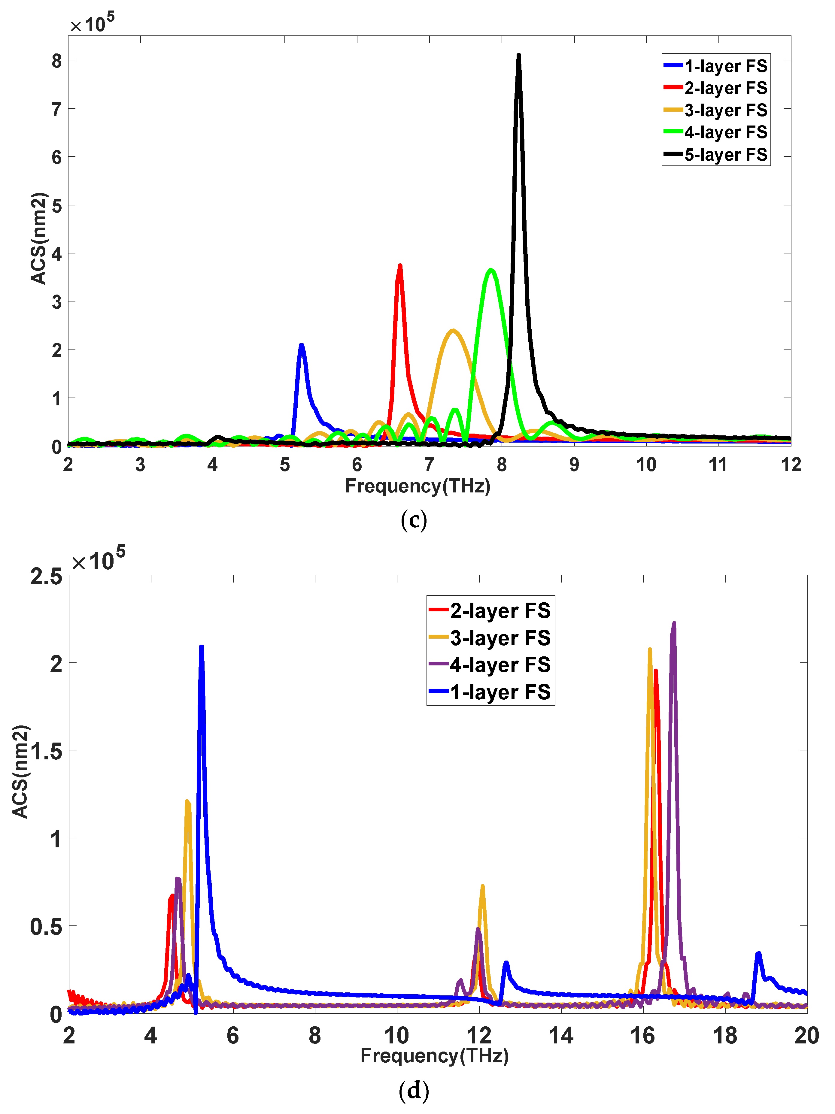
| Number of Graphene Layers Embedded | Single-Layer | Double-Layer | Three Layers | Four Layers | Five Layers |
|---|---|---|---|---|---|
| Plasmonic Frequency (THz) | 5.2285 | 6.5962 | 7.3387 | 7.84669 | 8.2375 |
| The Amplitude of Absorption Peak (×105 nm2) | 2.0892 | 3.7326 | 2.38817 | 3.64856 | 8.09279 |
| Bandwidth of Absorption Response (GHz) (Approximately) | 123.9 | 116.2 | 460 | 360 | 110 |
| Number of Graphene Layers Embedded | Single-Layer | Double-Layer | Three Layers | Four Layers |
|---|---|---|---|---|
| Plasmonic Frequency (THz) | 5.2285 | 4.5251 16.3086 | 4.875 12.0872 16.1663 | 4.63828 11.9689 16.7575 |
| The Amplitude of Absorption Peak (×105 nm2) | 2.0892 | 0.6711 1.953 | 1.2086 0.72523 2.07626 | 3.64856 0.48141 0.76625 |
| The Bandwidth of Absorption Response (GHz) (Approximately) | 123.9 | 142 134 | 157 140 130 | 140 140 150 |
| Angular Rotation of Graphene Sheet (°) | 0 | 0.5 | 1 | 1.5 |
|---|---|---|---|---|
| Plasmonic Frequency (THz) | 3.19639 | 3.31363 | 3.58717 | 3.66533 |
| The Amplitude of Absorption Peak (×104 nm2) | 8.43154 | 9.11228 | 10.35872 | 11.16 |
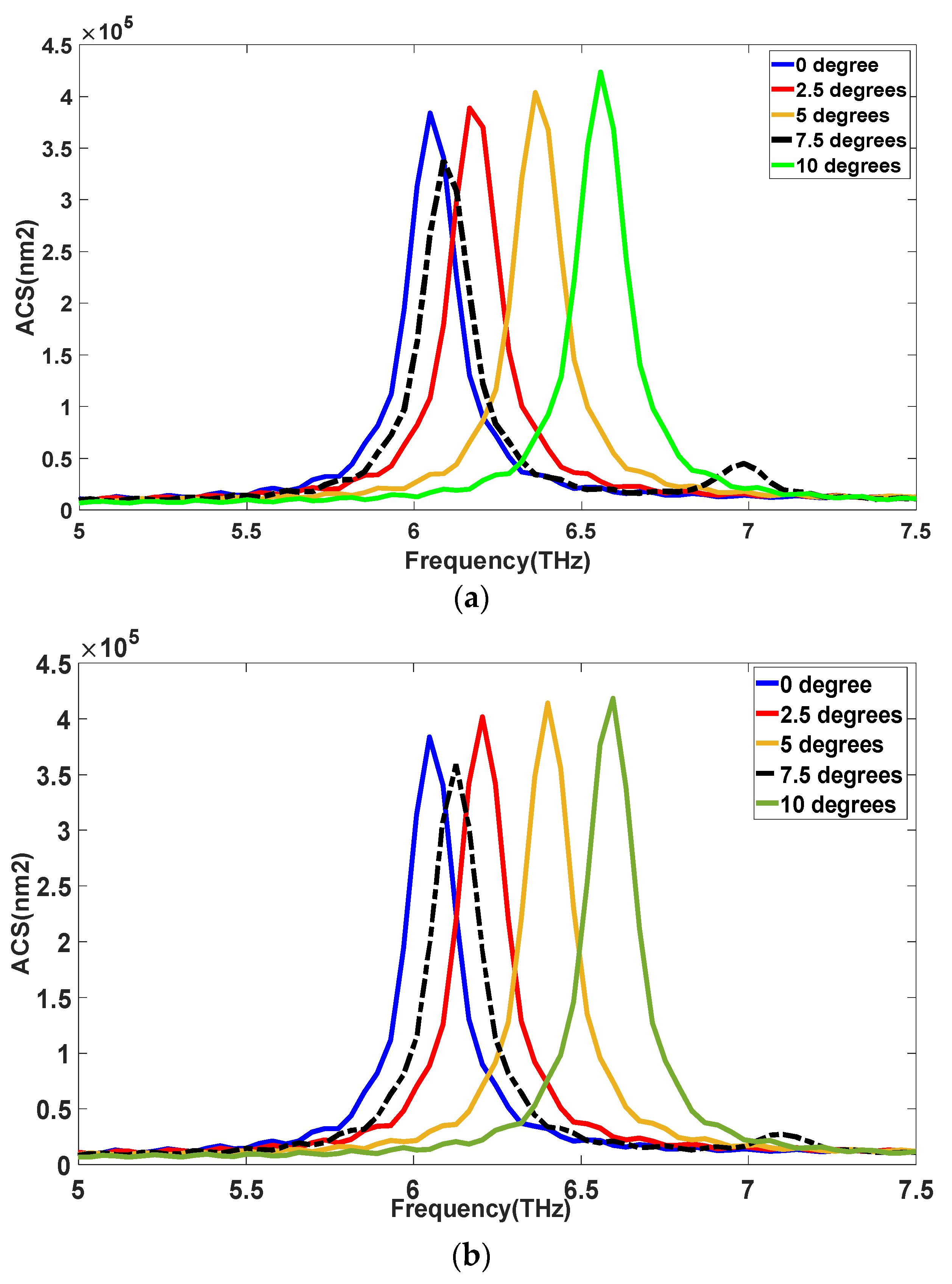
| Angular Rotation of Graphene Sheet (°) | 0 | 2.5 | 5 | 7.5 | 10 |
|---|---|---|---|---|---|
| Plasmonic Frequency (THz) | 6.0491 | 6.16633 | 6.36172 | 6.08818 | 6.55711 |
| The Amplitude of Absorption Peak (×104 nm2) | 3.83525 | 3.88302 | 4.03278 | 3.37791 | 4.23259 |
| Angular Rotation of Graphene Sheet (°) | 0 | 2.5 | 5 | 7.5 | 10 |
|---|---|---|---|---|---|
| Plasmonic Frequency (THz) | 6.0491 | 6.20541 | 6.4008 | 6.12725 | 6.59619 |
| The Amplitude of Absorption Peak (×104 nm2) | 3.83525 | 4.01656 | 4.13524 | 3.58740 | 4.18106 |
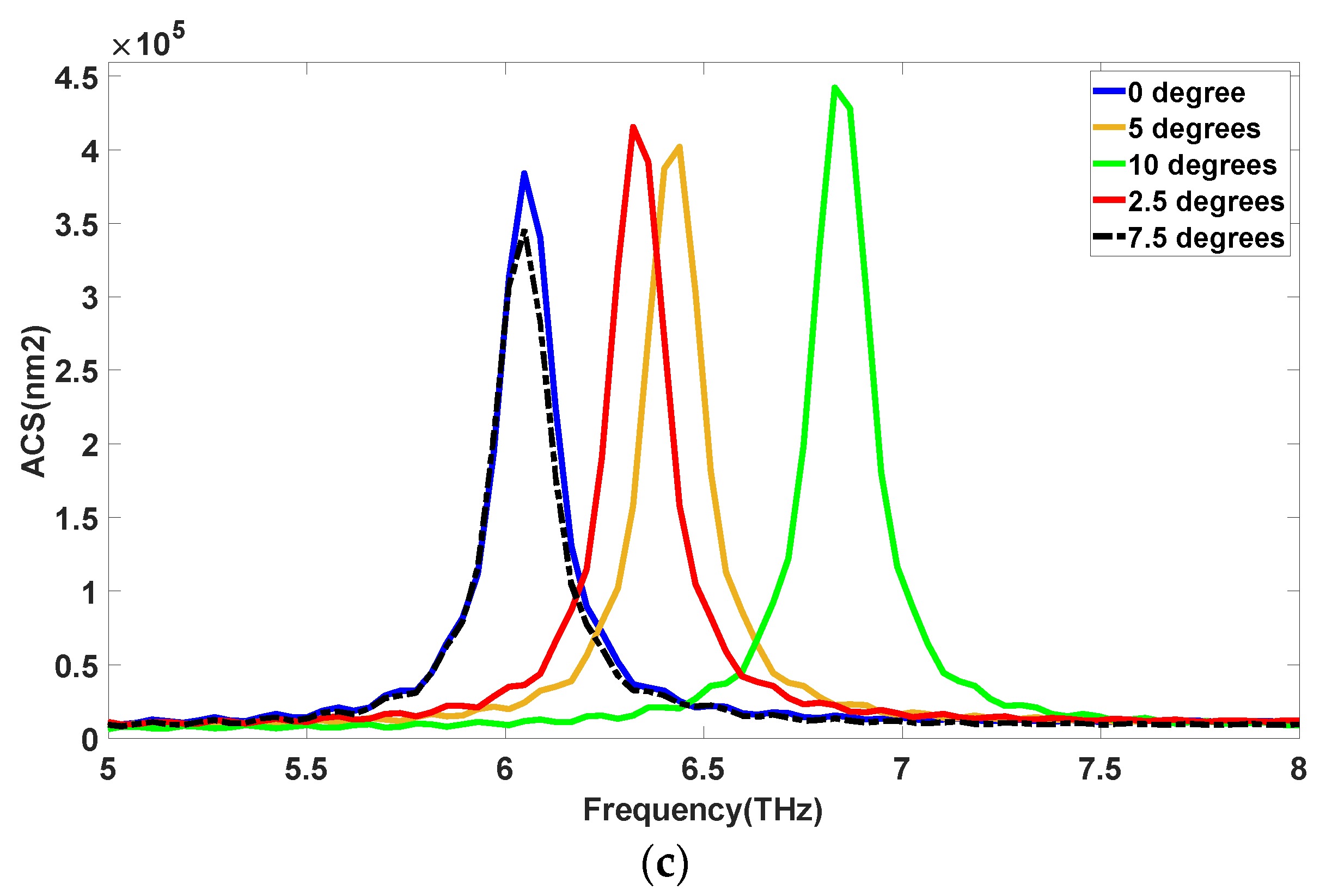
| Angular Rotation of Graphene Sheet (°) | 0 | 2.5 | 5 | 7.5 | 10 |
|---|---|---|---|---|---|
| Plasmonic Frequency (THz) | 6.0491 | 6.3226 | 6.43988 | 6.0491 | 6.83066 |
| The Amplitude of Absorption Peak (×104 nm2) | 3.83525 | 4.15166 | 4.01461 | 3.45296 | 4.4154 |
Publisher’s Note: MDPI stays neutral with regard to jurisdictional claims in published maps and institutional affiliations. |
© 2021 by the authors. Licensee MDPI, Basel, Switzerland. This article is an open access article distributed under the terms and conditions of the Creative Commons Attribution (CC BY) license (https://creativecommons.org/licenses/by/4.0/).
Share and Cite
Maghoul, A.; Rostami, A.; Gnanakulasekaran, N.; Balasingham, I. Design and Simulation of Terahertz Perfect Absorber with Tunable Absorption Characteristic Using Fractal-Shaped Graphene Layers. Photonics 2021, 8, 375. https://doi.org/10.3390/photonics8090375
Maghoul A, Rostami A, Gnanakulasekaran N, Balasingham I. Design and Simulation of Terahertz Perfect Absorber with Tunable Absorption Characteristic Using Fractal-Shaped Graphene Layers. Photonics. 2021; 8(9):375. https://doi.org/10.3390/photonics8090375
Chicago/Turabian StyleMaghoul, Amir, Ali Rostami, Nilojan Gnanakulasekaran, and Ilangko Balasingham. 2021. "Design and Simulation of Terahertz Perfect Absorber with Tunable Absorption Characteristic Using Fractal-Shaped Graphene Layers" Photonics 8, no. 9: 375. https://doi.org/10.3390/photonics8090375