Article

Multispectral Photonic Jet Shaping and Steering by Control of Tangential Electric Field Component on Cuboid Particle

1
Department of Biomedical Engineering, National Yang Ming Chiao Tung University, Taipei 112, Taiwan
2
School of Nondestructive Testing, Tomsk Polytechnic University, 634050 Tomsk, Russia
3
Institute for Strategic Studies, Siberian State University of Geosystems and Technologies, 630010 Novosibirsk, Russia
*
Author to whom correspondence should be addressed.
Photonics 2021, 8(8), 317; https://doi.org/10.3390/photonics8080317
Submission received: 29 June 2021 / Revised: 25 July 2021 / Accepted: 4 August 2021 / Published: 6 August 2021
(This article belongs to the Special Issue Photonic Devices and Systems)

Abstract

:
In this study, we present the simulations and experimental observations of photonic jet (PJ) shaping by control of tangential electric field components at illuminating wavelengths of 405 nm, 532 nm, and 671 nm. The PJs are generated by a single dielectric 4-micrometer cube that was fabricated from polydimethylsiloxane (PDMS). The dielectric cube is deposited on a silicon substrate and placed on two aluminum masks with a width equal to the side length of the cube. Due to the appearance of the metal masks, the focal length and decay length of the generated PJs decreased almost twice, while the PJ resolution increased 1.2 times. Thus, PJ shaping can be controlled by the presence of the metal mask along the lateral surface of the cube without changing the external shape or internal structure of the cube. This effect is based on the control of the tangential components of the electric field along the lateral surface of the cube. In the case of a one-sided metal mask, the effect of optical deflection and bending is predicted to form a photonic hook. Due to the low cost of these dielectric cubes, they have potential in far-field systems to better meet the requirements of modern optical integration circuits and switches.

1. Introduction

To form a photonic jet (PJ) with the required properties, several parameters of a low-loss dielectric particles can be changed, including the shape, size, material, and refractive index contrast [1,2,3,4]. Moreover, Mie size parameter q of a dielectric particle must correspond to q ~ (2…40)π, where q = 2πr/λ, r is the radius of the particle and λ is the incident wavelength [2]. The problem of the PJ beam shaping included several methods is considered in the literature. The influence of specific wavefront shaping illumination for SiO2 and BaTiO3 spherical particles is presented in the geometrical optics approximation conditions, i.e., with a diameter of the particles about q ~ 100π [5,6]. It is shown that the bending of axial field intensity distributions is similar to a classical lens with a decentered aperture due to the relatively large spherical aberration [7]. Among others, the PJ beam shaping methods include light polarization manipulation [8,9], illuminating wavefront structure [10,11], particle material compositions [12,13,14,15], sphere and cuboid particle apodization [16,17,18], and the shadow surface of particle nanostructuring [19,20]. These PJ beam shaping methods have a lot in common. The field intensity distributions of the PJ shape depend significantly on the optical properties and size of the generating particle materials as well as the shape and polarization state of illuminating waves [21]. Additionally, the modulation of PJ properties by dielectric spherical and cuboid particles surrounded with ideally conducting thin masks has been theoretically investigated [22]. It is observed that the effect of a thin mask on the PJ properties depends on the mask position along with the dielectric particles. However, there are very limited and clearly insufficient investigations of the role of tangential electric field components in the spatial and electromagnetic properties of the PJ. It could be noted that, in recent years, the studies in the field of the PJ effect based on the wavelength-scaled dielectric particles have gained more and more popularity and have found numerous applications, including optical trapping [23], nano-fabrications, and surface nano-patterning [24], quantum dot writing [25], microsphere-assisted microscopy and interferometry [26,27], auxiliary optomechanical manipulation [28], surface-enhanced Raman scattering [29], optical waveguides and switching [30,31], and biosensing [32], to name a few.
In this work, we present the PJ beam shaping generated by a particle of dielectric micro-cube (DMC) in the presence of the metal masks with the mask width equal to the side length of the DMC. The cubic particle shape with dimensions close to the incident wavelength is selected because it makes it possible to manufacture particles with a small number of defects and good quality [33]. Based on the experiments and finite-difference time-domain (FDTD) simulations, it is shown that both the PJ beam lateral width and length decrease by placing two metal masks along the cubic particle side. For this reason, we study the main parameters of the PJ such as full-width at half-maximum (FWHM), propagation length, and maximal field intensity distribution for a mesoscale cuboid particle in both free space and the presence of the metal masks. The designed DMC has been fabricated for measuring its focusing properties. A scanning optical microscope estimates the focusing performances in the visible light region at three wavelengths of 405 nm, 532 nm, and 671 nm. The experimental results are in reasonable agreement with simulation predictions. The suggested DMC with metal masks may open a new direction for both scientific researches and future industrial applications.

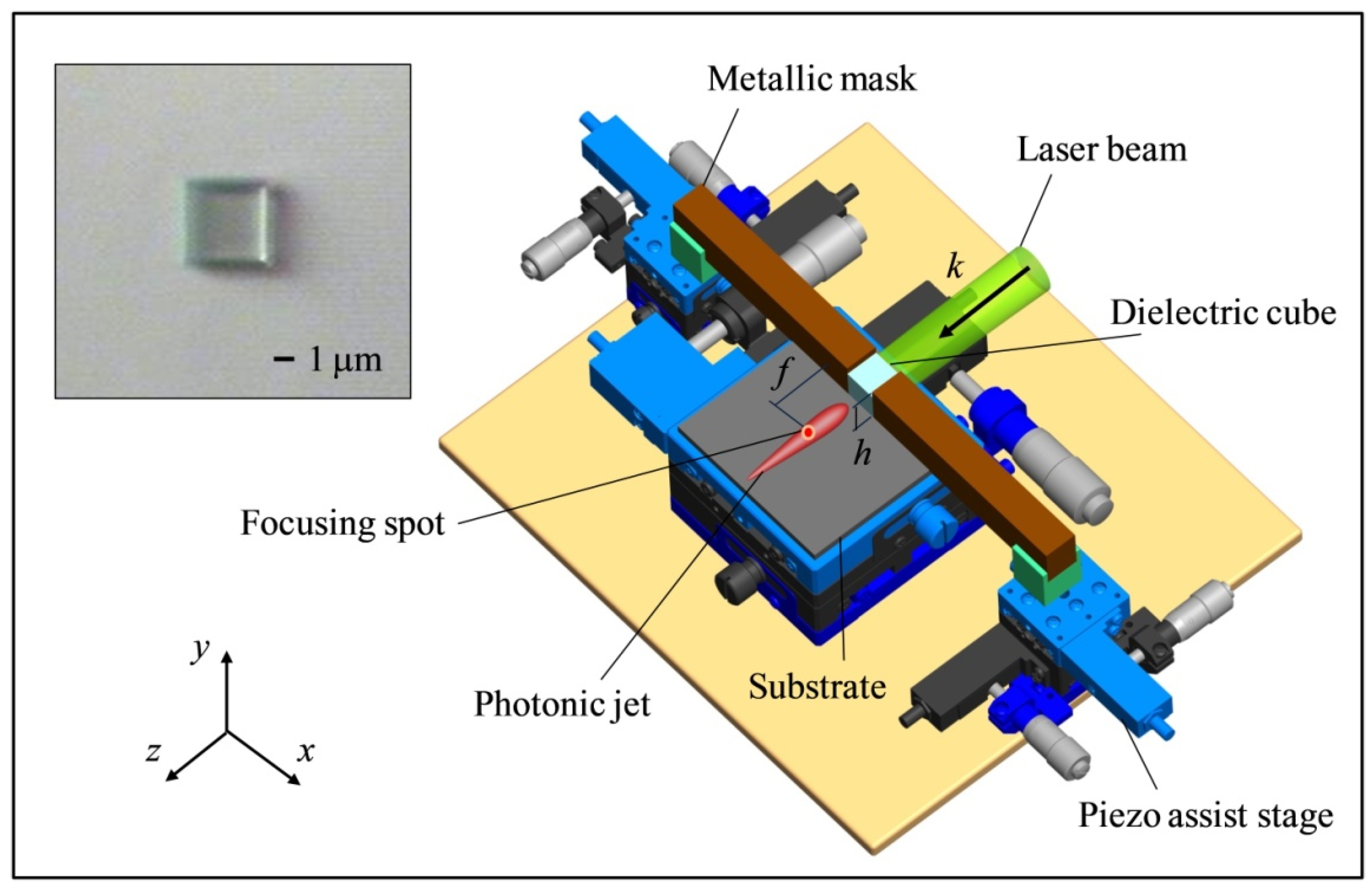
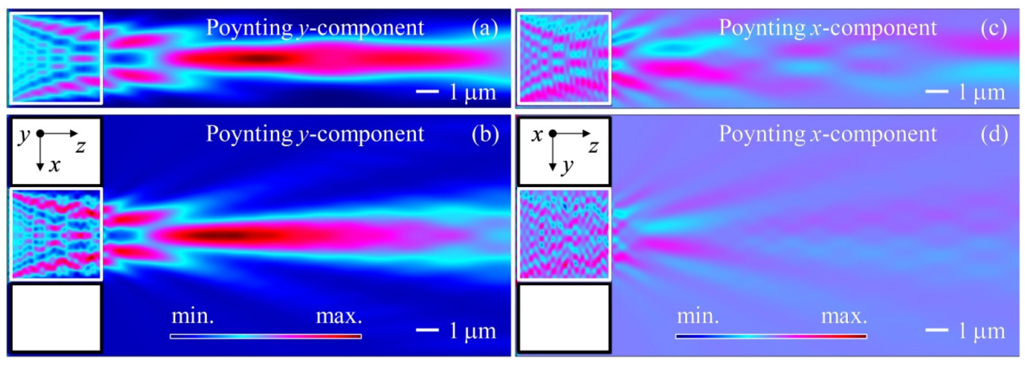
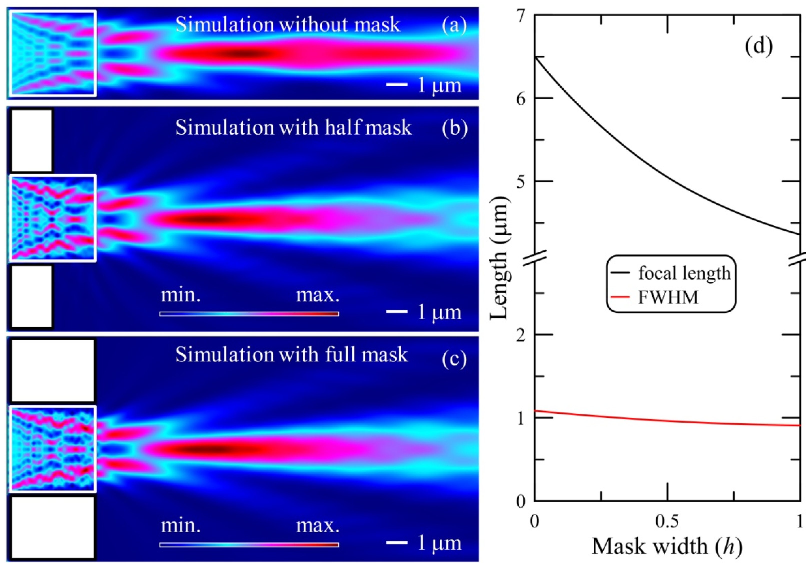
2. Methods and Results

The schematic of the studied system and the parameter definitions for the PJ with metal masks are shown in Figure 1. We exhibit the artistic representation of the DMC with two metal masks for generating PJ. The width, height (h), and length of the DMC are about 4 μm × 4 μm × 4 μm, which corresponds to the condition of q < 10π. Because an illuminated Gaussian beam with a breadth of 1 mm is much bigger than the DMC dimensions, the laser beam can be regarded as a quasi-plane wavefront. The DMC was placed on a silicon substrate with a refractive index of 4.15 + 0.05i, and the DMC material was polydimethylsiloxane (PDMS) with a refractive index of 1.43. We study numerically and experimentally the production capability of the PJ using the DMC illuminated by a laser beam without and with the metallic masks. The two equal aluminum masks with a width equal to the side length of the cube are positioned close to the DMC side surface. The wave vector of illuminating laser beam is in the positive x-direction. The spatial field intensity distributions are examined in the x-z plane near the shadow surface of the DMC.
The main parameters of the PJ include focal length, FWHM, decay length, and maximum peak intensity (MPI). The focal length f is defined as the distance from the DMC shadow surface to the point of MPI along the z-axis, and the decay length is defined as the distance from the MPI to the point at which the field intensity decays to 1/e time along the z-axis. We used the FDTD method with a mesh size of λ/20 to simulate the spatial field intensity distribution near the shadow surface of the DMC with and without metal masks [34,35]. The perfectly matched layers boundary conditions were implemented in the rigorous 2D FDTD simulation area. The insert in Figure 1 shows the microscopy photograph of the fabricated dielectric structure on a substrate. The selection of the PDMS material is an example of the DMC because it can be easily fabricated by replica molding technology and lithography [36]. The hole-type micro-pattern was created on a bare substrate by using a mask aligner and exposure apparatus. The hole-type pattern was operated for casting PDMS cube as a pattern transfer agent. We injected a liquid PDMS mixture into the hole-type pattern and then put another bare substrate upon it. After baking at 85 °C for 20 min, the solidified PDMS cube was obtained from the hole-type pattern. Some details of the technological process may be found in References [21,37]. A scanning optical microscope system was used to measure the focusing performances of the DMC with and without metal masks. The laser beam source was a diode-pumped solid-state linearly polarized laser with wavelengths of 405 nm, 532 nm, and 671 nm. A CMOS camera with high resolution is used to capture the direct images of field intensity distributions from the top view of the DMC. The DMC was placed on a two-axis piezo-assist stage (Sigma Koki, Tokyo, Japan, TADC-402WSPA) with 20 nm resolution. The technical details of the scanning optical microscope system can be found in Reference [38].
Figure 2 shows the experimental raw images and corresponding FDTD simulations (made in free space without dielectric support) for the DMC without metal masks at three incident wavelengths. The simulations and experimental results are in reasonable agreement. The discrepancies between the simulations and the experiments in Figure 2 are due to the influence of the substrate in the experiments, which the DMC is placed on [37]. As seen from the figures, the presence of a dielectric substrate imposes oscillating behavior to the field intensity distributions in experiments due to multiple field reflections from the silicone substrate and non-constructive interference [39,40]. In both the experiments and the simulations, it is clearly seen that an increase in the wavelength of the illuminating radiation from 405 nm to 671 nm leads to a decrease in the propagation length and the focal length. This is due to the fact that the effective size of the DMC decreases with increasing incident wavelength [41].
Figure 3 shows the experimental raw images for the DMC with two metal masks at the same three incident wavelengths in comparison to FDTD simulations. In the case of the DMC with metal masks, both the propagation length and the focal length decrease with an increase in the wavelength of the illuminating radiation from 405 nm to 671 nm. Comparing Figure 2 and Figure 3 indicates that the presence of the metal masks influences the focusing properties of the DMC. As shown in Figure 3, the range of field intensity distributions is reduced when the metal masks are placed on the side surface of the DMC. Meanwhile, the PJ length increases as the incident wavelength decreases, but the PJ width decreases as the incident wavelength decreases. As the engineered DMC with metal masks exhibits a high-concentration PJ, the field intensity distributions in Figure 3 support the conclusion regarding the contribution of the metal mask to the PJ. The proposed DMC with metal masks can work at several adjacent wavelengths.
Figure 4 shows the normalized intensity profiles of the PJs in the propagation direction and transverse direction for the DMC without and with metal masks at wavelengths of 405 nm, 532 nm, and 671 nm. The intensities for all DMCs with and without metal masks are normalized to the maximum intensity from the DMC at an incident wavelength of 405 nm. It can be clearly seen that when the DMC is placed with metal masks, the peak of the field intensity in the propagation direction shifts to the left towards the shadow surface of the DMC, and the width of the field intensity distributions at the focus plane also decreases by about 20%. In the simulations and experiments, the length, width, and MPI of the PJ depend on the presence of metal masks. More importantly, the focusing parameters of the PJ are tuned in both the z- and y-directions by placing the masks near the side faces of the DMC. The nature of considered effects is described by tangential field components during the formation of the PJ [22]. In the presence of the metal masks alongside the DMC faces, a reflected wave appears because the field component disappears at the contact area. As a result of reflection, the amplitude of the tangential electric field component increases in the direction opposite to that of wave propagation and weakens in the direction of wave propagation. These effects lead to the displacement of the power flow density concentration area across and in the direction of wave propagation. The PJ moves from the far side to the near surface of the DMC by placing two metal masks.
It is especially necessary to illustrate the spatial position, length, and width of the PJ. Figure 5 summarizes the PJ characteristics without and with the presence of metal masks at different wavelengths. At a fixed wavelength, all main parameters (focal length, FWHM, decay length) of the PJ are reduced in the presence of the metal mask. For example, the focal length decreases 1.8 times (from 7.5 μm to 4.2 μm), decay length decreases 1.7 times, and the resolution (FWHM) increases 1.2 times at an incident wavelength of 671 nm. It can be observed in Figure 5a that the focal length is a nearly linear enlargement with the decrease in incident wavelength. As a result, the focal length of the PJ can be adjusted by the metal masks, which could be a great benefit for practical applications. The DMC with metal masks is appropriate for detecting nano-scale targets away from the DMC surface. In Figure 5b, the FWHM decreases as incident wavelength decreases. The smallest FWHM is obtained for the DMC with metal masks for size parameter q = 9.87π at an incident wavelength of 405 nm. In this work, the height (h = 4 μm) of the DMC is chosen as an example. By properly selecting the DMC dimension, the considered DMC can be employed to overcome the diffraction limit at the beam focusing [26]. The PJ characteristics (focal length and location) can be drastically modulated by controlling the size parameter q of the DMC. For example, we may employ a PDMS cube to detect the existence of slight nano-targets (particles or films) inside or outside the PDMS cube. The DMC with metal masks generates the PJ with high intensity and spatial concentration. The nanoparticle inspections in the visible light region can be realized by the backscattering enhancement of the PJ.
Optical wavelength-scaled focusing elements occupy a key role in photonic applications. One of the most fundamental functions of such optical devices is light switching. The development of the PJ generation with chip-scale controllability of the beam steering and deflecting is important for a wide range of modern applications including optical communication [42], switch [43], and laser printers [44]. A composite photonic crystal composed of square and rectangular lattices is used to construct an artificial lasing band edge, which determines the direction of an optical beam. The laser devices based on such composite photonic crystal constructions may emit optical beams over a range of orientations, which can be dynamically and continuously controlled by the on-chip photonic integrated circuit. However, the shape of such composite photonic crystal structure is complex, making it very difficult to manufacture for practical applications. Therefore, we offer a novel concept to realize the possibility of the PJ steering using controllability of tangential electric field components.
In order to demonstrate PJ beam steering by control of the tangential electric field component, Figure 6 shows the simulation results of the DMC with only a one-side metal mask at incident wavelength of 532 nm. The start and inflection points are located at MPI/e on the left and right sides of MPI along the propagation direction (z or z1 axes). The effects of a shift in the focal length and the PJ deflection on the presence of the one-sided metal mask are clearly noticeable. In the case of placing the mask on only one side of the DMC, the curved PJ not only deflects by an angle of about 5° (angle between the z and z1 axes) but also acquires a slight curvature. The original type of such curved PJ is known as a photonic hook (PH) [45]. Figure 6c shows the intensity profiles from the energy flux density distributions in the z and z1 directions. In the intensity profile along the z-axis, it can be seen that the inflection point (point A) is observed corresponding to the beginning of the PJ curvature at a distance of about 13 μm from the DMC surface. Compared with the intensity profile along the changed direction (z1-axis), the inflection point (point B) shifts at the distance of about 15 μm (about 28λ), which indicates the appearance of the curvature of the formed PJ. The asymmetric interference structure of the localized field distributions along the radiation propagation axis is also clearly visible, which manifests the effect on the presence of a one-sided mask.
The control of the tangential electric field component is carried out by using a metal mask placed along the dielectric side surfaces of a cubic particle, which has a thickness greater than the thickness of the skin layer [22]. For ease of experimental demonstration of this effect, we employ a thick mask with a width equal to the cubic size in this study. In contrast, the effect of a thin mask has been demonstrated in Reference [22]. The two components of the Poynting vectors for the DMC without and with masks are considered to clarify the effect of the thick mask on the PJ shaping. Figure 7 shows the simulation results of Poynting y- and x-components of the power flow patterns for the DMC without and with metal masks. The reflected waves appear in the presence of thick masks alongside the particle faces because the field component disappears at the contact zone. As shown in Figure 7c,d, the amplitude of the tangential electric field component declines in the propagation direction and increases in the opposite direction of the wave propagation. The details of the displacement of the power flow density concentration region across and in the propagation direction have been described in Reference [22]. It can be seen from Figure 7a,b that the PJ intensity distribution varies from the sword type to the dagger type. The PJ location moves near the DMC surface by placing two metal masks. To illustrate the effect of the mask width on the PJ shaping, Figure 8 shows the simulation results of the power flow patterns for the DMC with metal masks of zero, half-width, and full width at 671 nm incident wavelength. It was observed that by increasing the mask width from zero to the cubic length, the focal length reduces from 6.51 μm to 4.36 μm and the FWHM of the PJ is nearly constant. In the future, we may use an integrated electronic circuit to manipulate the position of the metal masks, enabling advanced focusing beam control. For example, any desired angled focusing beams and their on-demand modulation could be realized by the DMC with metal masks.

3. Conclusions

In conclusion, we directly observed experimental effects of the PJ shaping and steering in the multispectral visible light at the wavelengths of 405 nm, 532 nm, and 671 nm for the DMC with size parameters of q = 9.87π, 7.52π, and 5.96π in the presence of the metal masks along both 1- and 2-lateral surfaces of the DMC. It was demonstrated experimentally and numerically that a number of main parameters of the generated PJ can be controlled by the presence of the metal mask along the DMC lateral surface without changing the external shape or internal structure of the DMC. The modulation effect is based on the control of the tangential electric field components along the DMC surface. It is shown that the length and lateral width of the PJ shape decrease upon placing two metal masks along DMC side surfaces. In the case of a one-sided metal mask, the deflection and bending of the formed PJ (PH) are observed from the power flow patterns. The deflection angle can be tuned almost linearly by tuning the position of a metal mask along one side of the DMC. The PJ beam deflection and steering may play a key role in laser micromachining [46], imaging applications [47,48,49] including optical microscopy based on cantilever combined with microparticle [50] and nano-manipulation [51]. Finally, we believe that the described method of the PJ parameters control should be inherent to other types of beams and frequency bands, including surface waves and microwaves. This study will have a wide-reaching influence on a range of practical applications, including chip-to-chip optical communication and laser scalpels embedded in capsules for medical treatments.

Author Contributions

Conceptualization, O.V.M. and I.V.M.; methodology, O.V.M., I.V.M. and C.-Y.L.; software, C.-Y.L. and W.-Y.C.; validation, C.-Y.L. and W.-Y.C.; formal analysis, O.V.M. and I.V.M.; resources, C.-Y.L.; data curation, W.-Y.C.; writing—original draft preparation, O.V.M. and I.V.M.; writing—review and editing, C.-Y.L.; visualization, C.-Y.L. and W.-Y.C.; supervision, O.V.M. and I.V.M.; project administration, C.-Y.L.; funding acquisition, O.V.M., I.V.M., and C.-Y.L. All authors have read and agreed to the published version of the manuscript.

Funding

This research was funded by the Ministry of Science and Technology of Taiwan (MOST 108-2221-E-010-012-MY3, MOST 109-2923-E-010-001-MY2), Yen Tjing Ling Medical Foundation (CI-110-28), and Russian Foundation for Basic Research (20-57-S52001).

Institutional Review Board Statement

Not applicable.

Informed Consent Statement

Not applicable.

Data Availability Statement

The data that support the findings of this study are available from the corresponding author upon reasonable request.

Acknowledgments

This research was supported by the TPU development program.

Conflicts of Interest

The authors declare no conflict of interest.

References

  1. Heifetz, A.; Kong, S.; Sahakian, A.; Taflove, A.; Backman, V. Photonic nanojets. J. Comput. Theor. Nanosci. 2009, 6, 1979–1992. [Google Scholar] [CrossRef]
  2. Luk’yanchuk, B.; Paniagua-Domínguez, R.; Minin, I.V.; Minin, O.V.; Wang, Z. Refractive index less than two: Photonic nanojets yesterday, today and tomorrow. Opt. Mater. Express 2017, 7, 1820–1847. [Google Scholar] [CrossRef]
  3. Zhu, J.; Goddard, L. All-dielectric concentration of electromagnetic fields at the nanoscale: The role of photonic nanojets. Nanoscale Adv. 2019, 1, 4615–4643. [Google Scholar] [CrossRef] [Green Version]
  4. Lin, C.; Lee, Y.; Liu, C. Optimal photonic nanojet beam shaping by mesoscale dielectric dome lens. J. Appl. Phys. 2020, 127, 243110. [Google Scholar] [CrossRef]
  5. Wang, F.; Liu, L.; Yu, P.; Liu, Z.; Yu, H.; Wang, Y.; Li, W. Three-dimensional super-resolution morphology by near-field assisted white-light interferometry. Sci. Rep. 2016, 6, 24703. [Google Scholar] [CrossRef] [PubMed] [Green Version]
  6. Xing, E.; Gao, H.; Rong, J.; Khew, S.; Liu, H.; Tong, C.; Hong, M. Dynamically tunable multi-lobe laser generation via multifocal curved beam. Opt. Express 2018, 26, 30944–30951. [Google Scholar] [CrossRef]
  7. Avendaño-Alejo, M.; Castañeda, L.; Moreno, I. Properties of caustics produced by a positive lens: Meridional rays. J. Opt. Soc. Am. A 2010, 27, 2252–2260. [Google Scholar] [CrossRef]
  8. Chen, R.; Lin, J.; Jin, P.; Cada, M.; Ma, Y. Photonic nanojet beam shaping by illumination polarization engineering. Opt. Commun. 2020, 456, 124593. [Google Scholar] [CrossRef]
  9. Liu, Y.; Wang, B.; Ding, Z. Influence of incident light polarization on photonic nanojet. Chin. Opt. Lett. 2011, 9, 072901. [Google Scholar]
  10. Kiselev, A.; Plutenko, D. Mie scattering of Laguerre-Gaussian beams: Photonic nanojets and near-field optical vortices. Phys. Rev. A 2014, 89, 043803. [Google Scholar] [CrossRef] [Green Version]
  11. Yousefi, M.; Scharf, T.; Rossi, M. Photonic nanojet generation under converging and diverging beams. J. Opt. Soc. Am. B 2021, 38, 317–326. [Google Scholar] [CrossRef]
  12. Liu, C.; Yen, T.; Minin, O.V.; Minin, I.V. Engineering photonic nanojet by a graded-index micro-cuboid. Physica E 2018, 98, 105–110. [Google Scholar] [CrossRef]
  13. Zhen, Z.; Huang, Y.; Feng, Y.; Shen, Y.; Li, Z. An ultranarrow photonic nanojet formed by an engineered two-layer microcylinder of high refractive-index materials. Opt. Express 2019, 27, 9178–9188. [Google Scholar] [CrossRef]
  14. Huang, Y.; Zhen, Z.; Shen, Y.; Min, C.; Veronis, G. Optimization of photonic nanojets generated by multilayer microcylinders with a genetic algorithm. Opt. Express 2019, 27, 1310–1325. [Google Scholar] [CrossRef] [PubMed]
  15. Liu, C. Flexible photonic nanojet formed by cylindrical graded-index lens. Crystals 2019, 9, 198. [Google Scholar] [CrossRef] [Green Version]
  16. Wu, M.; Chen, R.; Soh, J.; Shen, Y.; Jiao, L.; Wu, J.; Chen, X.; Ji, R.; Hong, M. Super-focusing of center-covered engineered microsphere. Sci. Rep. 2016, 6, 31637. [Google Scholar] [CrossRef] [PubMed] [Green Version]
  17. Yue, L.; Yan, B.; Monks, J.; Wang, Z.; Tung, N.; Lam, V.; Minin, O.V.; Minin, I.V. Production of photonic nanojets by using pupil-masked 3D dielectric cuboid. J. Phys. D Appl. Phys. 2017, 50, 175102. [Google Scholar] [CrossRef]
  18. Yue, L.; Yan, B.; Monks, J.; Wang, Z.; Tung, N.; Lam, V.; Minin, O.V.; Minin, I.V. A millimetre-wave cuboid solid immersion lens with intensity-enhanced amplitude mask apodization. J. Infrared Millim. Terahertz Waves 2018, 39, 546–552. [Google Scholar] [CrossRef] [Green Version]
  19. Wu, M.; Chen, R.; Ling, J.; Chen, Z.; Chen, X.; Ji, R.; Hong, M. Creation of a longitudinally polarized photonic nanojet via an engineered microsphere. Opt. Lett. 2017, 42, 1444–1447. [Google Scholar] [CrossRef]
  20. Cao, Y.; Liu, Z.; Minin, O.V.; Minin, I.V. Deep subwavelength-scale light focusing and confinement in nanohole-structured mesoscale dielectric spheres. Nanomaterials 2019, 9, 186. [Google Scholar] [CrossRef] [Green Version]
  21. Liu, C.; Lin, F. Geometric effect on photonic nanojet generated by dielectric microcylinders with non-cylindrical cross-sections. Opt. Commun. 2016, 380, 287–296. [Google Scholar] [CrossRef]
  22. Dorofeev, I.; Suslyaev, V.; Minin, O.V.; Minin, I.V. Role of the tangential electric field component to the terahertz jet and hook formation by dielectric cube and sphere. Opt. Eng. 2021, 60, 082004. [Google Scholar] [CrossRef]
  23. Lu, D.; Pedroni, M.; Labrador-Páez, L.; Marqués, M.; Jaque, D.; Haro-González, P. Nanojet trapping of a single sub-10 nm upconverting nanoparticle in the full liquid water temperature range. Small 2021, 17, 2006764. [Google Scholar] [CrossRef] [PubMed]
  24. Surdo, S.; Duocastella, M.; Diaspro, A. Nanopatterning with photonic nanojets: Review and perspectives in biomedical research. Micromachines 2021, 12, 256. [Google Scholar] [CrossRef]
  25. Ristori, A.; Hamilton, T.; Toliopoulos, D.; Felici, M.; Pettinari, G.; Sanguinetti, S.; Gurioli, M.; Mohseni, H.; Biccari, F. Photonic jet writing of quantum dots self-aligned to dielectric microspheres. Adv. Quantum Technol. 2021, 2100045. [Google Scholar] [CrossRef]
  26. Abbasian, V.; Moradi, A. Microsphere-assisted super-resolved Mueller matrix microscopy. Opt. Lett. 2020, 45, 4336–4339. [Google Scholar] [CrossRef] [PubMed]
  27. Hüser, L.; Lehmann, P. Microsphere-assisted interferometry with high numerical apertures for 3D topography measurements. Appl. Opt. 2020, 59, 1695–1702. [Google Scholar] [CrossRef] [PubMed]
  28. Minin, I.V.; Minin, O.V.; Cao, Y.; Liu, Z.; Geints, Y.; Karabchevsky, A. Optical vacuum cleaner by optomechanical manipulation of nanoparticles using nanostructured mesoscale dielectric cuboid. Sci. Rep. 2019, 9, 12748. [Google Scholar] [CrossRef] [PubMed] [Green Version]
  29. Gašparic, V.; Taccheo, S.; Gebavi, H.; Ristic, D.; Ivanda, M. Photonic nanojet mediated Raman enhancement: Vertical Raman mapping and simple ray matrix analysis. J. Raman Spectrosc. 2020, 51, 165–175. [Google Scholar] [CrossRef]
  30. Liu, C.; Minin, O.V.; Minin, I.V. Periodical focusing mode achieved through a chain of mesoscale dielectric particles with a refractive index near unity. Opt. Commun. 2019, 434, 110–117. [Google Scholar] [CrossRef]
  31. Geints, Y.; Minin, O.V.; Yue, L.; Minin, I.V. Wavelength-scale photonic space switch proof-of-concept based on photonic hook effect. Ann. Phys. 2021, 2100192. [Google Scholar] [CrossRef]
  32. Li, Y.; Liu, X.; Xu, X.; Xin, H.; Zhang, Y.; Li, B. Red-blood-cell waveguide as a living biosensor and micromotor. Adv. Funct. Mater. 2019, 29, 1905568. [Google Scholar] [CrossRef]
  33. Zhou, B.; Dong, H.; Jiang, M.; Zheng, W.; Sun, L.; Zhao, B.; Tang, B.; Pan, A.; Zhang, L. Single-mode lasing and 3D confinement from perovskite micro-cubic cavity. J. Mater. Chem. C 2018, 6, 11740–11748. [Google Scholar] [CrossRef]
  34. Taflove, A.; Hagness, S. Computational Electrodynamics: The Finite Difference Time Domain Method; Artech House: Boston, MA, USA, 2005. [Google Scholar]
  35. Liu, C. Photonic jets produced by dielectric micro cuboids. Appl. Opt. 2015, 54, 8694–8699. [Google Scholar] [CrossRef]
  36. Shih, T.; Chen, C.; Ho, J.; Chuang, F. Fabrication of PDMS (polydimethylsiloxane) microlens and diffuser using replica molding. Microelectron. Eng. 2006, 83, 2499–2503. [Google Scholar] [CrossRef]
  37. Minin, I.V.; Liu, C.; Yang, Y.; Staliunas, K.; Minin, O.V. Experimental observation of flat focusing mirror based on photonic jet effect. Sci. Rep. 2020, 10, 8459. [Google Scholar] [CrossRef] [PubMed]
  38. Liu, C.; Li, C. Photonic nanojet induced modes generated by a chain of dielectric microdisks. Optik 2016, 127, 267–273. [Google Scholar] [CrossRef]
  39. Moreno, F.; Saiz, J.; González, F. Light scattering by particles on substrates. Theory and experiments. In Light Scattering and Nanoscale Surface Roughness; Maradudin, A., Ed.; Springer: Boston, MA, USA, 2007; pp. 305–340. [Google Scholar]
  40. Minin, I.V.; Minin, O.V.; Pacheco-Peña, V.; Beruete, M. Localized photonic jets from flat, three-dimensional dielectric cuboids in the reflection mode. Opt. Lett. 2015, 40, 2329–2332. [Google Scholar] [CrossRef]
  41. Minin, I.V.; Minin, O.V. Diffractive Optics and Nanophotonics; Springer: Berlin/Heidelberg, Germany, 2016. [Google Scholar]
  42. Kurosaka, Y.; Iwahashi, S.; Liang, Y.; Sakai, K.; Miyai, E.; Kunishi, W.; Ohnishi, D.; Noda, S. On-chip beam-steering photonic-crystal lasers. Nat. Photonics 2010, 4, 447–450. [Google Scholar] [CrossRef]
  43. Singh, O.; Paulus, R. A critical review of optical switches. J. Opt. Commun. 2021, in press. [Google Scholar] [CrossRef]
  44. Matsuda, T.; Abe, F.; Takahashi, H. Laser printer scanning system with a parabolic mirror. Appl. Opt. 1978, 17, 878–884. [Google Scholar] [CrossRef]
  45. Minin, I.V.; Minin, O.V.; Liu, C.; Wei, H.; Geints, Y.; Karabchevsky, A. Experimental demonstration of tunable photonic hook by partially illuminated dielectric microcylinder. Opt. Lett. 2020, 45, 4899–4902. [Google Scholar] [CrossRef] [PubMed]
  46. Gattass, R.; Mazur, E. Femtosecond laser micromachining in transparent materials. Nat. Photonics 2008, 2, 219–225. [Google Scholar] [CrossRef]
  47. Betzig, E.; Trautman, J. Near-field optics: Microscopy, spectroscopy, and surface modification beyond the diffraction limit. Science 1992, 257, 189–195. [Google Scholar] [CrossRef] [PubMed] [Green Version]
  48. Delaney, P.; Harris, M.; King, R. Fiber-optic laser scanning confocal microscope suitable for fluorescence imaging. Appl. Opt. 1994, 33, 573–577. [Google Scholar] [CrossRef] [PubMed]
  49. Lechleiter, J.; Lin, D.; Sieneart, I. Multi-photon laser scanning microscopy using an acoustic optical deflector. Biophys. J. 2002, 83, 2292–2299. [Google Scholar] [CrossRef] [Green Version]
  50. Wang, S.; Zhang, D.; Zhang, H.; Han, X.; Xu, R. Super-resolution optical microscopy based on scannable cantilever-combined microsphere. Microsc. Res. Tech. 2015, 78, 1128–1132. [Google Scholar] [CrossRef]
  51. Zhang, T.; Yu, H.; Li, P.; Wang, X.; Wang, F.; Shi, J.; Liu, Z.; Yu, P.; Yang, W.; Wang, Y.; et al. Microsphere-based super-resolution imaging for visualized nanomanipulation. ACS Appl. Mater. Interfaces 2020, 12, 48093–48100. [Google Scholar] [CrossRef]
Figure 1. Geometrical description of the photonic jet generation by the dielectric cube with metal masks. The insert indicates the microphotograph of the single dielectric cube on a substrate.
Photonics 08 00317 g001
Figure 2. Simulation results of the power flow patterns for the dielectric cube without mask at incident wavelengths of (a) 405 nm, (b) 532 nm, and (c) 671 nm. Experimental raw images of the dielectric cube without mask at incident wavelengths of (d) 405 nm, (e) 532 nm, and (f) 671 nm.
Photonics 08 00317 g002
Figure 3. Simulation results of the power flow patterns for the dielectric cube with metal masks at incident wavelengths of (a) 405 nm, (b) 532 nm, and (c) 671 nm. Experimental raw images of the dielectric cube with metal masks at incident wavelengths of (d) 405 nm, (e) 532 nm, and (f) 671 nm.
Photonics 08 00317 g003
Figure 4. Normalized intensity profiles of the photonic jets in the propagation direction for the dielectric cube (a) without and (b) with metal masks. The origin of the propagation direction is located at the cube surface. Normalized intensity profiles of the photonic jets in the transverse direction for the dielectric cube (c) without and (d) with metal masks. The insert indicates the locations of the propagation direction and the transverse direction.
Photonics 08 00317 g004
Figure 5. Main parameters as a function of incident wavelength for photonic jets: (a) focal length, (b) FWHM, and (c) decay length.
Photonics 08 00317 g005
Figure 6. Simulation results of the power flow patterns for a cube with masks on (a) two sides and (b) one side. (c) Intensity profiles of the photonic jets in the propagation direction for the dielectric cube with two and one metallic masks. The origin of the propagation direction is located at the cube surface.
Photonics 08 00317 g006
Figure 7. Poynting y-component of the power flow patterns for the dielectric cube (a) without and (b) with metal masks. Poynting x-component of the power flow patterns for the dielectric cube (c) without and (d) with metal masks.
Photonics 08 00317 g007
Figure 8. Simulation results of the power flow patterns for the dielectric cube with metal masks of (a) zero, (b) half width, and (c) full width at incident wavelength of 671 nm. (d) Focal length and FWHM as a function of the screen width for the PJ.
Photonics 08 00317 g008
Publisher’s Note: MDPI stays neutral with regard to jurisdictional claims in published maps and institutional affiliations.

