Article

Structural and Optical Properties of InAsSbBi Grown by Molecular Beam Epitaxy on Offcut GaSb Substrates

by
Rajeev R. Kosireddy
1,
Stephen T. Schaefer
2,
Marko S. Milosavljevic
2,3,4 and
Shane R. Johnson
2,*
1
Center for Photonics Innovation & School for Engineering of Matter, Transport, and Energy, Arizona State University, Tempe, AZ 85287, USA
2
Center for Photonics Innovation & School of Electrical, Computer, and Energy Engineering, Arizona State University, Tempe, AZ 85287, USA
3
Air Force Research Laboratory, Space Vehicles Directorate, Kirtland Air Force Base, Albuquerque, NM 87117, USA
4
Applied Technology Associates, Albuquerque, NM 87123, USA
*
Author to whom correspondence should be addressed.
Photonics 2021, 8(6), 215; https://doi.org/10.3390/photonics8060215
Submission received: 14 April 2021 / Revised: 4 June 2021 / Accepted: 9 June 2021 / Published: 11 June 2021
(This article belongs to the Special Issue Near- and Mid-Infrared Photonics Technologies)

Abstract

:
Three InAsSbBi samples are grown by molecular beam epitaxy at 400 °C on GaSb substrates with three different offcuts: (100) on-axis, (100) offcut 1° toward [011], and (100) offcut 4° toward [011]. The samples are investigated using X-ray diffraction, Nomarski optical microscopy, atomic force microscopy, transmission electron microscopy, and photoluminescence spectroscopy. The InAsSbBi layers are 210 nm thick, coherently strained, and show no observable defects. The substrate offcut is not observed to influence the structural and interface quality of the samples. Each sample exhibits small lateral variations in the Bi mole fraction, with the largest variation observed in the on-axis growth. Bismuth rich surface droplet features are observed on all samples. The surface droplets are isotropic on the on-axis sample and elongated along the [ 01 1 ¯ ] step edges on the 1° and 4° offcut samples. No significant change in optical quality with offcut angle is observed.

1. Introduction

High-speed, highly sensitive optoelectronic devices such as photodetectors and lasers operating in the mid- and long-wave infrared spectrum are desired for applications including navigation, night vision, missile detection, communication, imaging, and spectroscopy [1]. Alloying bismuth extends the performance of III-V compounds into the mid- and long-wave infrared range without incurring high levels of detrimental strain. For example, alloying bismuth in InAs reduces the room-temperature bandgap energy by 51 meV/% Bi [2], a much greater rate than alloying Sb, which reduces the bandgap energy by 9.3 meV/% Sb [3]. InAsSbBi lattice-matched to commercially available GaSb substrates spans bandgap energies from 0.32 to 0.10 eV (4 to 12 µm) at low temperature and 0.27 to 0.042 eV (5 to 30 µm) at room temperature [4]. Dilute III-V bismide alloys exhibit similarities to dilute nitride alloys such as GaAs1-xNx due to the large mismatch in atomic radii and electronegativity between Bi and N and the host III-V material [5,6]. In dilute nitride alloys, the highly electronegative N atoms introduce an impurity energy level near the host conduction band, resulting in splitting of the conduction band and a decrease in the band gap energy due to the band anti-crossing interaction [7,8,9,10]. In contrast, the smaller electronegativity of Bi results in an impurity energy level near the host material valence band and splitting of the valence band due to a similar band anti-crossing interaction [9,10,11,12,13,14]. Additionally, the band anti-crossing interaction due to Bi incorporation results in strong spin-orbit splitting in the valence band [9,15]. Bismuth incorporation shifts the valence band offset upwards, offering improved hole confinement compared to InAsSb alone [2,3]. Additionally, the extra degree of design freedom afforded by the quaternary InAsSbBi alloy provides independent control of the strain and bandgap. However, the large mismatch in atomic radii between Bi and the host InAsSb material makes the growth of high Bi content InAsSbBi challenging [4]. In general, this mismatch and the tendency for Bi to segregate on the growth surface leads to composition modulation and the formation of surface droplets during the growth of III-V-Bi materials [16,17,18,19,20,21,22,23]. In this work, the impact of substrate offcut on the growth and subsequent microstructural and optical properties of InAsSbBi is investigated.

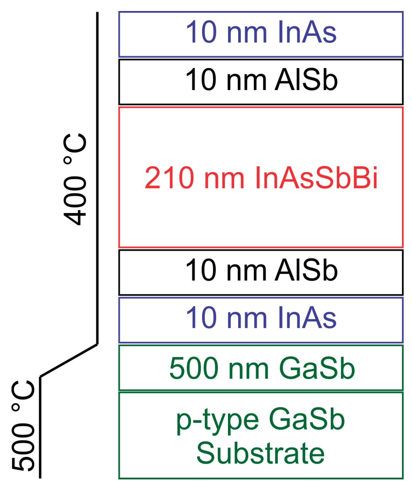
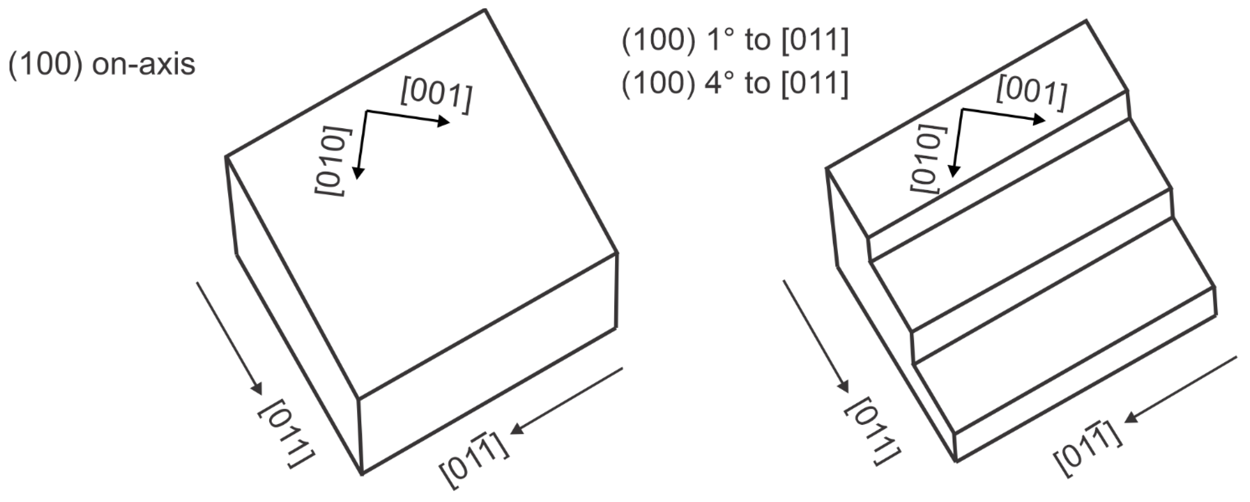
2. Materials and Methods

InAs1-x-ySbyBix, bulk layers grown by solid-source molecular beam epitaxy on vicinal GaSb were investigated for three different substrate offcuts, (100) on axis, (100) offcut 1° to [011], and (100) offcut 4° to [011]. The sample cross-section shown in Figure 1 consisted of a 500 nm GaSb buffer, a 10 nm InAs/10 nm AlSb partially strain balanced barrier, the InAsSbBi active region, and a terminating 10 nm AlSb/10 nm InAs barrier/cap layer. The InAs/AlSb barriers provided electrical confinement for the photogenerated carriers during photoluminescence measurements. The growth surface was prepared by first desorbing surface oxidation from the GaSb substrate in the growth chamber for approximately 15 min at 540 °C under Sb flux. The GaSb buffer layer was grown at 500 °C except for the last 70 nm, where the substrate temperature was reduced by 100 °C in preparation for the growth of the InAsSbBi active layer. The thermal removal of the surface oxide and the buffer growth was identical for all three samples and did not vary with substrate offcut. The InAsSbBi layers were grown at a temperature of 400 °C using relative group-V to In flux ratios of 0.911 for As/In, 0.105 and 0.120 for Sb/In, and 0.050 for Bi/In. Solid source valved arsenic and antimony cells with cracking zone temperatures of 990 and 750 °C, respectively, primarily provided As2 and Sb2 flux during the growth of InAsSbBi. A solid source valved Bi cell primarily provided monatomic Bi flux. Of the incident Bi flux, an average of about 72% desorbed, about 14% incorporated substitutionally in the group-V sublattice, and about 14% accumulated on the surface forming Bi rich droplets [24]. A constant In atom flux of 4.4 × 1014 cm−2s−1 corresponding to an InAsSbBi on GaSb growth rate of about 15 nm/min or 0.82 monolayers/s was used for all growths. The InAsSbBi layers and growth conditions are provided in Table 1.
The As/In and Sb/In fluxes were calibrated prior to each growth by growing InAs on InAs and InSb on InSb and lowering the V/In flux ratio until the transition from a group-V to a group-III rich surface reconstruction was observed using reflection and high energy electron diffraction. This procedure accurately and repeatably calibrated the one-to-one group-V to In flux ratios for As and Sb, from which ion gauge measurements of the As and Sb fluxes as a function of valve position were employed to set the flux with a precision better than 1%. The Bi flux was calibrated using scanning electron microscope measurements of the thickness of 190 nm of elemental Bi deposited on GaAs at 100 °C. All growths were performed under group-V-rich surface reconstructions. The individual group-V fluxes were established in terms of excess elemental overpressure, defined as the difference between the incident V/In flux ratio for a given element and the mole fraction of the element incorporated in the film. The substrate temperature was measured using an Ircon Modline 3 (model 3G-10C05) pyrometer.
A schematic of the surfaces of the on-axis and two offcut substrates is shown in Figure 2. The offcut in the [011] direction resulted in terraces and step edges that run along the [ 01 1 ¯ ] direction on the (100) surfaces. The wafer manufacturer [25] denoted the offcut directions as being (100) offcut toward (011) for sample B and (100) toward (111)A for sample C, which resulted in the surface being tilted toward [011] in both cases.
The structure and composition of InAsSbBi films were investigated using high-resolution X-ray diffraction (XRD) and transmission electron microscopy (TEM), while the surface morphology of the samples was examined using Nomarski optical microscopy and atomic force microscopy (AFM). The X-ray diffraction measurements were performed using a PANalytical X’Pert Pro MRD X-ray diffractometer with an instrumental resolution of 12 arcsec and Cu 1 radiation with a 1.54 Å wavelength. The X-ray diffraction measurements consisted of coupled ω - 2 θ triple-axis scans with measurement intervals spaced 3.6 arcsec apart around the symmetric (400) reflection. Slit widths of 1/2° and 1/4° were used on the incident and diffracted beams, respectively, with a #5 mask corresponding to an irradiated full width at half maximum of approximately 5 mm for the incident beam and a dwell time of 1 s at each measurement interval. Simulations of coupled diffraction scans were carried out using the PANalytical X’Pert Epitaxy [26] dynamical diffraction modeling software. The Nomarski images were acquired using an Olympus MX50 optical microscope with Nomarski prism, analyzer, and polarizer components. The AFM images we acquired using a Brucker multimode 8 microscope with a lateral scan range of 100 microns and a vertical scan range of 5.5 microns. Cross-sectional TEM samples were prepared in the [ 01 1 ¯ ] projections using wedge polishing followed by Ar-ion milling at liquid nitrogen temperature. TEM imaging was carried out using a Philips CM 200 microscope operating at 200 kV, with an interpretable resolution of 2.5 Å. Scanning TEM imaging was carried out using an aberration corrected JEOL ARM 200F operated at an acceleration voltage of 200 kV, with a spatial resolution of 0.8 Å.
The InAsSbBi samples were examined using temperature-dependent photoluminescence spectroscopy. The samples were mounted in a closed-loop He-refrigerated cryostat and optically pumped using a modulated 785 nm laser diode. The measurements were performed at temperatures ranging from 13 to 295 K using an average pump power of 100 mW that provided an active layer excitation density of 120 W/cm2. The photoluminescence was collected using a Nicolet Magna-IR 760 Fourier Transform infrared spectrometer with an InSb detector with a cutoff wavelength of 5.5 μm. The pump laser was modulated at 50 kHz, and the detector signal was fed through a phase-locked loop amplifier for improved signal-to-noise. The system optical throughput was measured and corrected using the spectrum from a Mikron M305 black body source at 800 °C.

3. Results

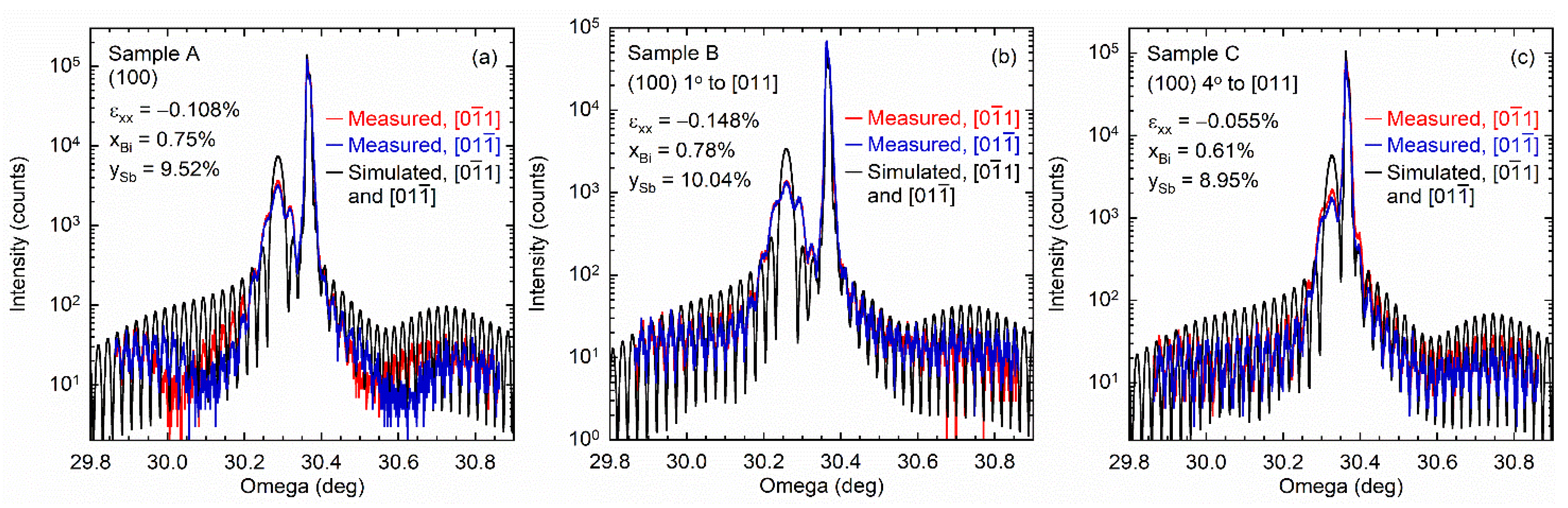
3.1. Examination of InAsSbBi Layers Using XRD

The coupled ω - 2 θ X-ray diffraction scans of the (004) reflection are plotted in Figure 3 as a function of diffraction angle θ , equal to the angle of incidence ω , for samples A, B, and C. The scans are measured along the [ 0 1 ¯ 1 ] direction (red curves) and [ 01 1 ¯ ] direction (blue curve), eliminating the effect of any crystallographic tilt on the measurement and enabling accurate determination of the InAsSbBi tetragonal distortion from coupled ω - 2 θ scans. Dynamical simulations of the scans using X’Pert Epitaxy [26] are shown as black curves. In the simulations, the InAsSbBi layer is assumed to be pseudomorphic as the lattice mismatch is sufficiently small that the critical thickness [27] significantly exceeds that of the InAsSbBi layer in all samples. Further, it is assumed that Poisson’s ratio is independent of the InAsSbBi layer composition and is given as 0.3522 [4]. The Bi and Sb mole fractions are adjusted in the simulation to match the angular separation of the InAsSbBi layer and GaSb substrate peaks, uniquely identifying the InAsSbBi lattice constant. The thickness of the InAsSbBi layer and the AlSb barrier layers are adjusted in the simulation to match the period and spacing, respectively, of the Pendellösung fringes, which arise from thin film X-ray interference. The thickness of the InAs layers is determined self-consistently from the InAsSbBi layer thickness based on a constant In deposition rate used throughout the growth. A tensile peak is observed near the GaSb substrate peak that is due to the unintentional incorporation of approximately 0.17% As in the GaSb buffer. The unintentional As originates from the As background pressure in the growth chamber and is too small to induce relaxation in the 500 nm-thick buffer layer.
The measured InAsSbBi layer peak is broadened and reduced in intensity compared to the simulations for all three samples. In addition, sideband peaks not predicted by the dynamical simulation are observed on both sides of the InAsSbBi layer peak. This is due to the presence of surface droplet features that are thought to scatter X-ray radiation away from the angular peak corresponding to the InAsSbBi lattice constant. This is evident from the examination of droplet-free InAsSbBi samples grown under similar conditions that exhibit much better agreement between the width and intensity of the measured and simulated InAsSbBi layer peaks [4,16].
A summary of the InAsSbBi epilayer results is provided in Table 2, including the simulated layer thickness, Bragg angle θ I n A s S b B i , out-of-plane distortion ε , lattice constant a I n A s S b B i , and in-plane biaxial strain ε x x , and the measured diffraction angle peak θ P e a k and the simulated diffraction angle peak θ s i m u l a t e d . The dynamical simulations provide the precise diffraction (Bragg) angle for the InAsSbBi layer that differs from the measured diffraction peak due to the presence of strong Pendellösung film interference fringes that can shift the diffraction angle peak in multilayered structures. The uncertainties provided for each parameter are based on the observed sensitivity of the match of the dynamical simulation to the measured diffraction pattern. The minimum observable change in Bi mole fraction in these simulations is 0.01%. The uncertainties of the other parameters follow from their relations to the change in Bi mole fraction.

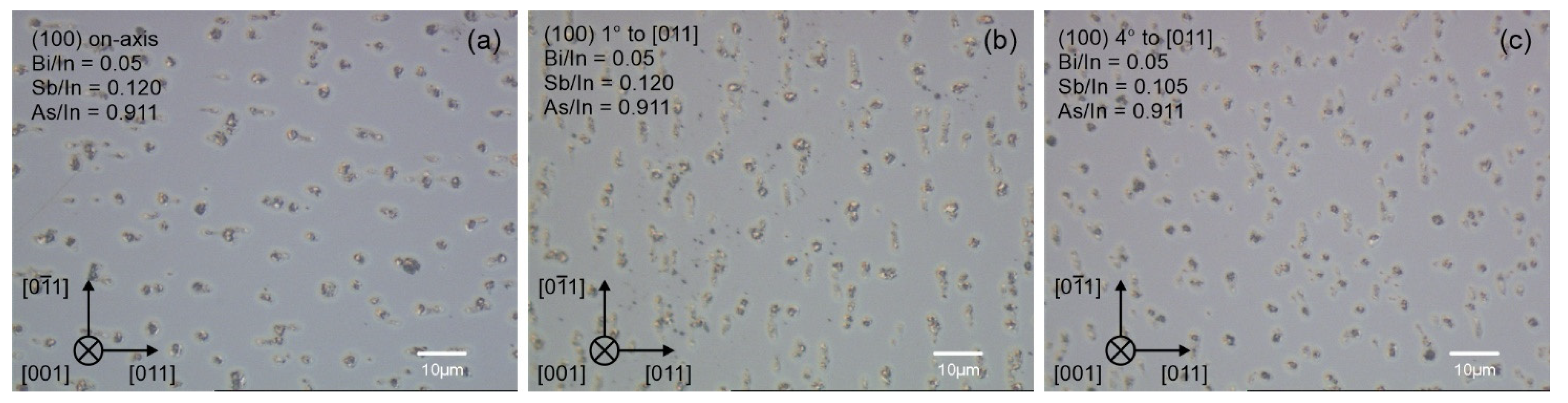
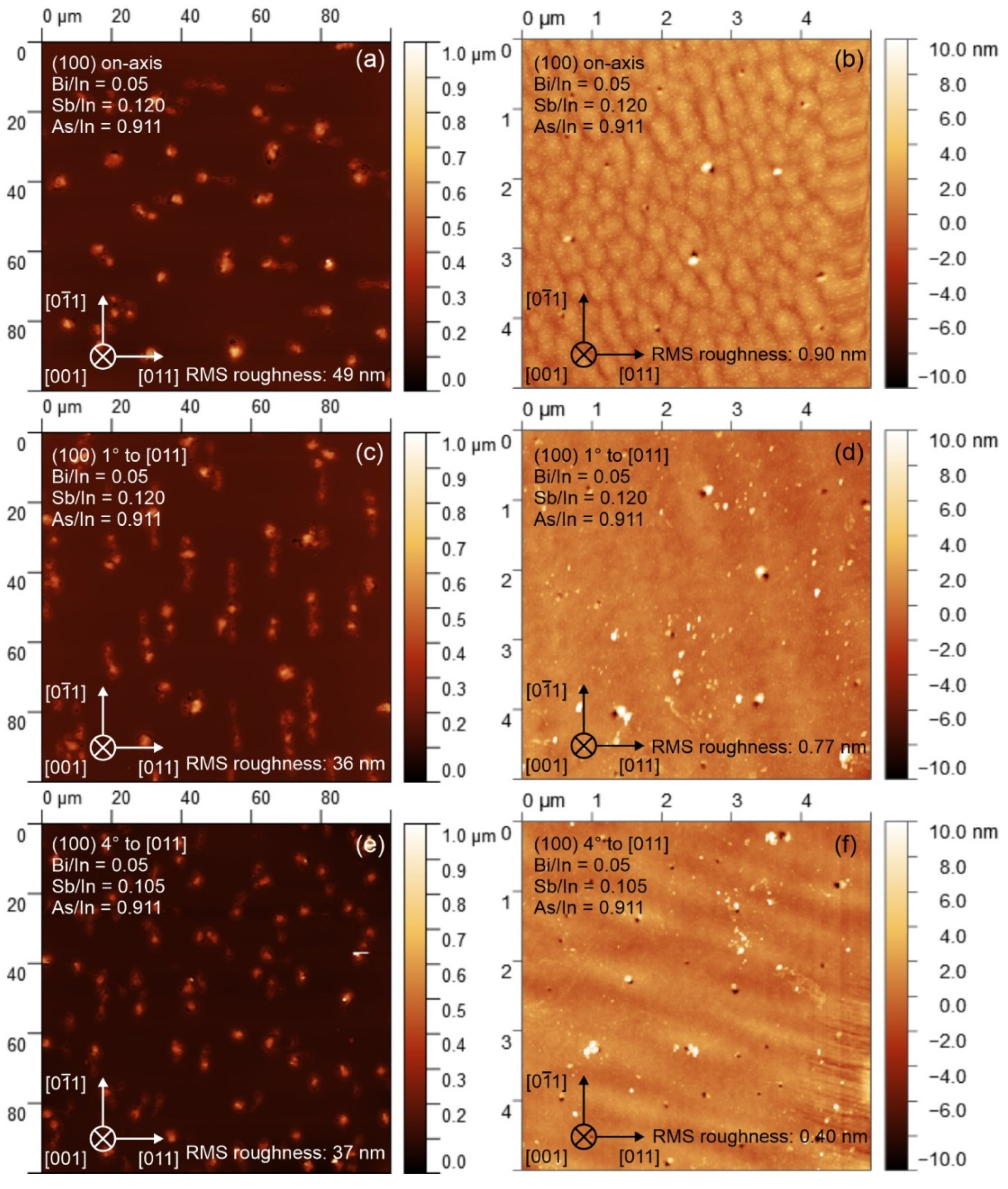
3.2. Surface Morphology of InAsSbBi Samples

The Nomarski optical microscopy images of the surface of the three InAsSbBi samples are shown in Figure 4. The images are 100 µm wide by 75 µm high and the significant growth conditions are shown for each. Surface droplet features are observed on all samples. These features have average diameters and densities, respectively, of 2.6 µm and 1.8 × 106 cm−2 in sample A, 2.1 µm and 2.4 × 106 cm−2 in sample B, and 1.9 µm and 3.2 × 106 cm−2 in sample C. Additionally, 1° offcut sample B (Figure 4b) with step edge density 5.7 × 105 cm−1 exhibits surface droplet features elongated in the [ 0 1 ¯ 1 ] direction, indicating preferential diffusion of the Bi and In atoms along the step edges. The 4° offcut sample C (Figure 4c) also exhibits preferential alignment of the droplet features along the [ 0 1 ¯ 1 ] direction, albeit to a lesser extent than in sample B. The droplet density and diameter measured from Nomarski images is reported in Table 4.
The atomic force microscopy images of the surface of the three InAsSbBi samples are shown in Figure 5. The images are 100 µm by 100 µm on the left with a magnified 5 µm by 5 µm measurement on the right. The root mean square (RMS) roughness of the area imaged is shown in Table 3. The size, density, height, and volume per unit area of the droplet features is analyzed using the Gwyddion software package [28]. With droplets over 200 nm high, the surfaces have a RMS roughness around 40 nm on the 100 µm length scale. The surface between the large droplet features is relatively smooth, with an RMS roughness over the 5 µm square region that decreases from 0.90 to 0.40 nm as the offcut angle increases from 0 to 4°.
The InAsSbBi layer thickness obtained from the dynamical simulations of the X-ray diffraction (XRD) pattern is significantly smaller than the growth target and hence indicates that in addition to excess Bi, a fraction of the incident In is consumed by the droplets during the Bi accumulation process [24]. The X-ray diffraction measurements provide a reliable measurement of the layer thickness and are used to determine the fraction of In lost to the droplets. The loss of material relative to the 210 nm target thickness is 16, 21, and 20 nm for samples A, B, and C, respectively. This thickness difference is due to metallic In accumulation in the droplet features. The total amount of In per unit area accumulated in the droplets is calculated directly from the thickness difference. The corresponding amount of metallic Bi per unit area contained within the droplets is given by the difference between the total volume per unit area of droplet features and the metallic In volume per unit area [24]. The results indicate that 18.9%, 9.2%, and 12.4% of the incident Bi flux and 3.5%, 4.6%, and 4.4% of the In flux accumulates in surface droplets in samples A, B, and C, respectively.
The droplet sizes and densities, fraction of the surface covered by droplets, and the droplet volume per unit area are reported in Table 4. Nomarski optical microscopy images do not measure droplet height, and therefore only droplet density, average diameter, and surface coverage fraction are reported for this method. The droplet counting and thresholding techniques used in Nomarski optical microscopy image analysis overestimate droplet density compared to atomic force microscopy analysis using the Gwyddion software [28].

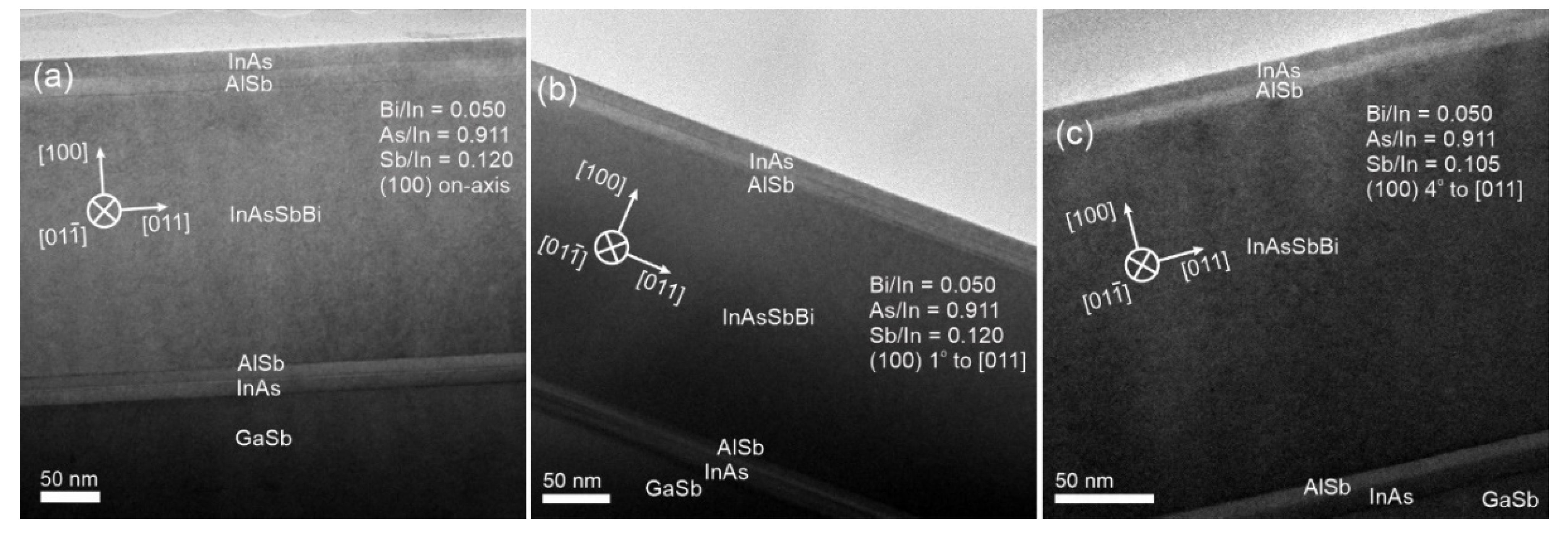
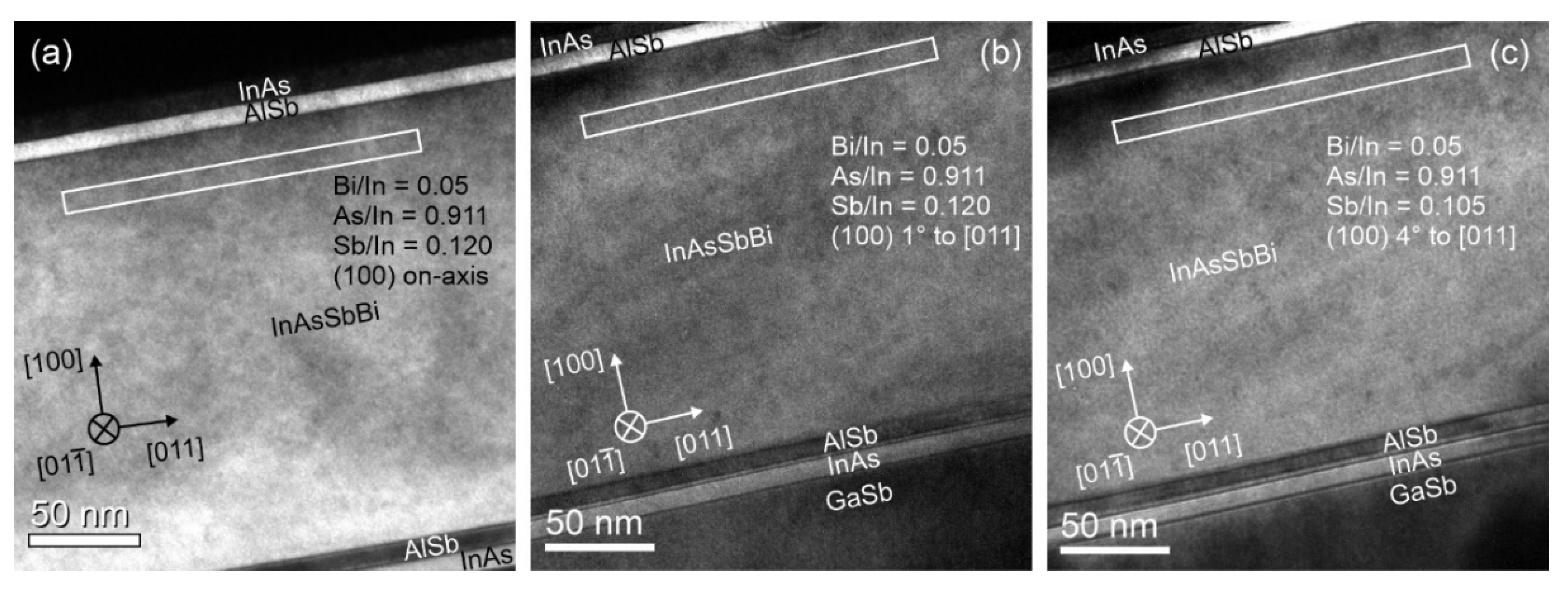
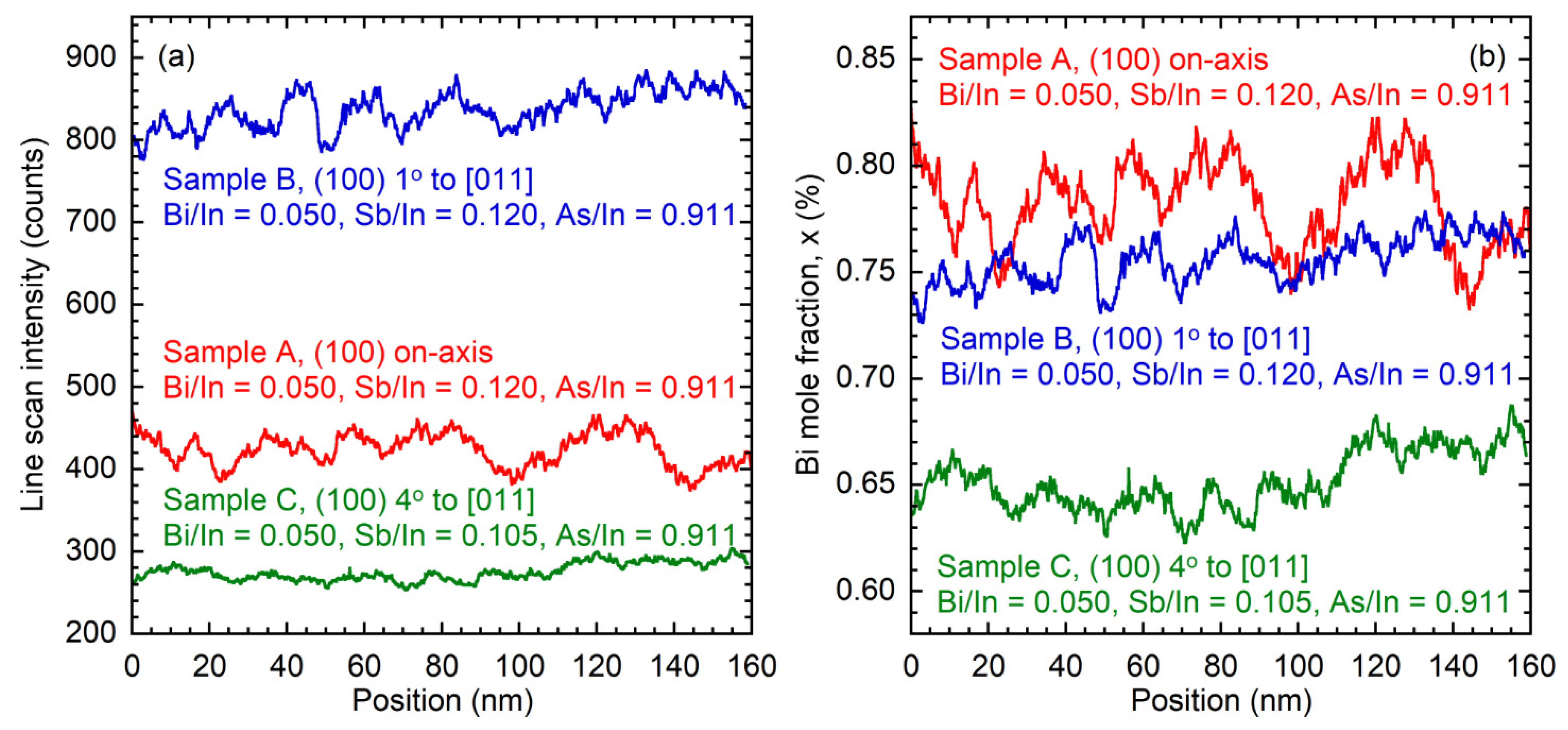
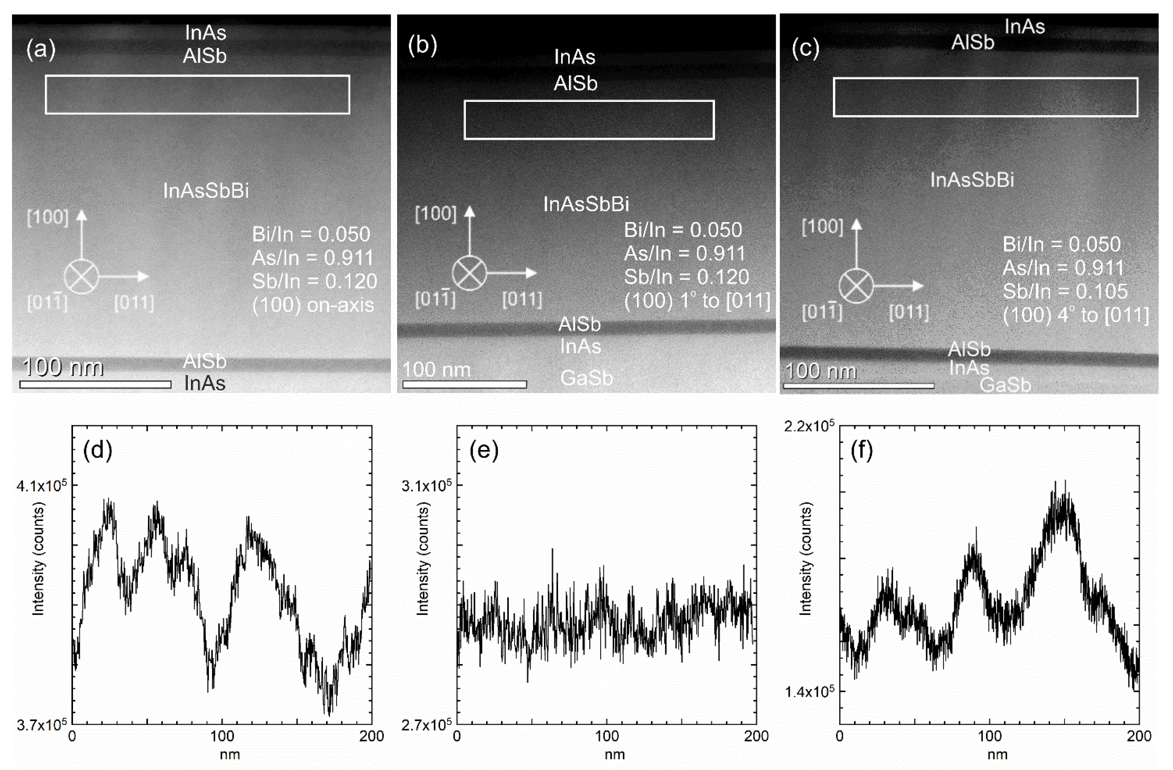
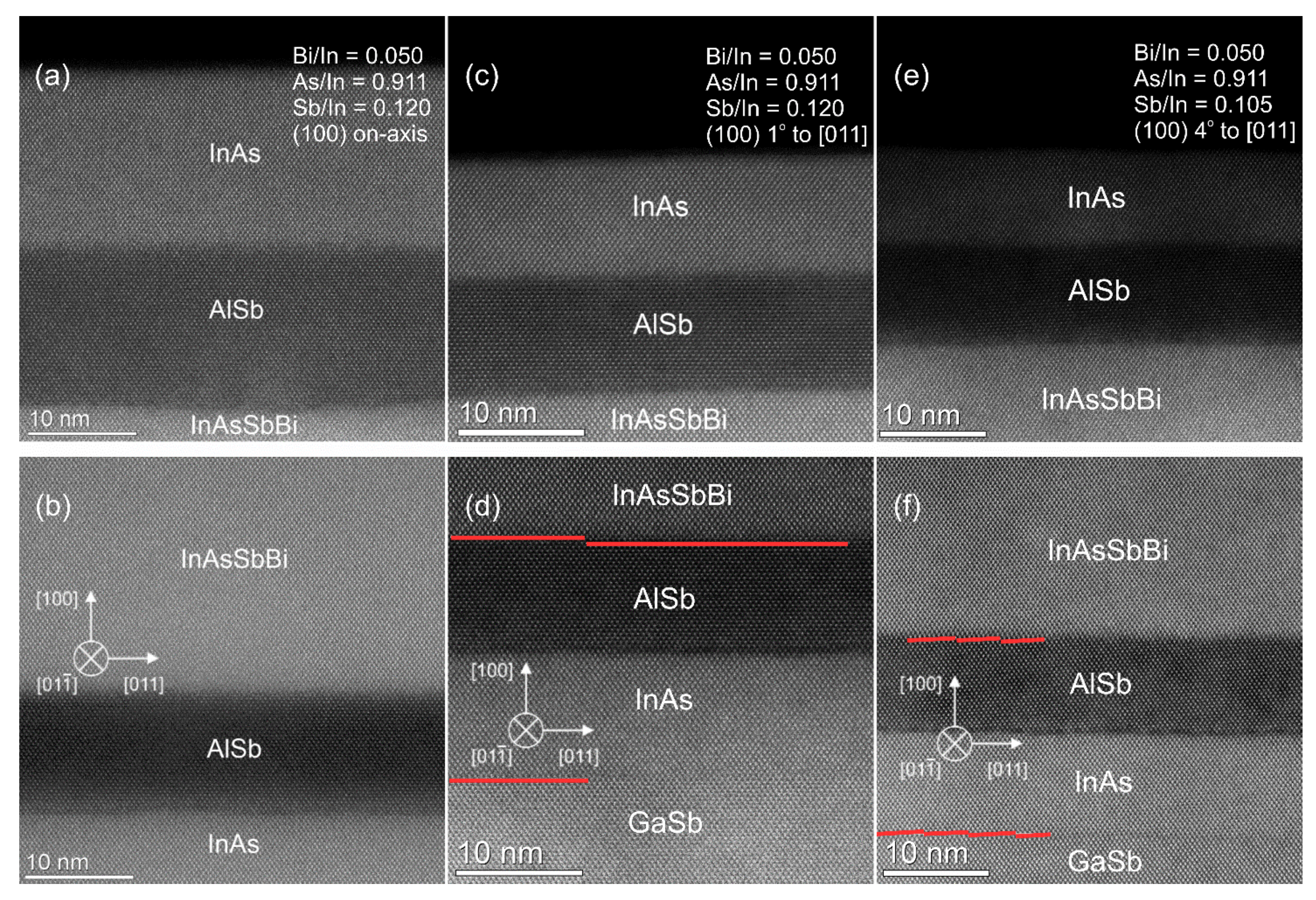
3.3. Examination of InAsSbBi Microstructure Using TEM

The overall microstructure of the InAsSbBi layers is examined using cross-sectional TEM. Low-magnification bright-field TEM micrographs from the three InAsSbBi samples are presented in Figure 6. The images indicate the InAsSbBi layers are pseudomorphic with no extended defects over the image scale. Contrast modulation due to varying chemical composition [16] with a period of approximately 30 nm is observed in samples A and C, as shown in Figure 6a,c, respectively. Lateral composition modulation is not observed in sample B in the bright-field TEM images (see Figure 6b).
Chemically sensitive (200) dark-field TEM micrographs of the InAsSbBi layers are presented in Figure 7. The contrast in the (200) dark-field images is sensitive to the elemental content of the layer and provides local chemical information. Bright areas in the InAsSbBi layer correspond to comparatively Bi-rich regions, while dark areas correspond to Bi-deficient regions. The dark-field image contrast changes with TEM specimen thickness in the [ 100 ] growth direction, which varies from 3 nm at the top of the epilayer to approximately 11 nm at the bottom. This is illustrated by the contrast reversal between the upper and lower AlSb and InAs layers; therefore local chemical information can only be obtained in the in the lateral [ 011 ] direction and not in the [ 100 ] growth direction.
The Bi mole fraction is calculated from the (200) dark-field images in Figure 7 using the method developed by Bithell and Stobbs [29] and applied to InAsSbBi by R. Kosireddy et al. [16]. The intensity of the dark-field reflection, I 200 , I n A s S b B i , is proportional to the specimen thickness d squared and the structure factor squared for the (200) reflection. The constant of proportionality and the specimen thickness are eliminated by comparing the ratio of intensity scattered by InAsSbBi into the (200) reflection with that scattered by AlSb at same the specimen thickness. The ratio of the intensities is given as [16]
I 200 , I n A s S b B i I 200 , A l S b = [ f I n ( 1 x y ) f A s y f S b x f B i ] [ f A l f S b ] 2 2 .
The Bi mole fraction is expressed in terms of this intensity ratio, the atomic scattering factors, the Sb mole fraction, and the ratio of the intensities, with
x = f A s f I n + ( f S b f A s ) y + ( f A l f S b ) I 200 , I n A s S b B i I 200 , A l S b f A s f B i .
The atomic scattering factors f A l , f I n , f A s , f S b , and f B i for Al, In, As, Sb, and Bi, respectively, are determined by linearly interpolating the values tabulated by Doyle and Turner [30] to the scattering angle parameter s = 1 / a for each sample, where a is the out-of-plane lattice constant of the InAsSbBi layer. The atomic scattering factors are listed in Table 5 and are weakly dependent on the InAsSbBi composition.
Lateral intensity profiles from the regions outlined by white rectangles in the dark-field images in Figure 7 are shown in Figure 8a. The subsequent Bi mole fraction profiles are shown in Figure 8b. The specimen cross sections examined are approximately 80 nm thick. The Bi mole fraction varies laterally from 0.73% to 0.83% with an average and range of 0.78 ± 0.05% in sample A, from 0.73% to 0.79% with an average and range of 0.76 ± 0.03% in sample B, and from 0.63% to 0.69% with an average and range of 0.65% +0.04/−0.02% in sample C.
The Sb mole fraction y is specified by the Bi mole fraction measured by TEM and the unstrained InAsSbBi lattice constant a I n A s S b B i determined from the XRD analysis using the linear relationship between mole fraction and lattice constant predicted by Vegard’s law [4,31], with
y = a I n A s S b B i a I n A s a I n S b a I n A s x   a I n B i a I n A s a I n S b a I n A s = 2.3747   Å 1 ( a I n A s S b B i 6.0583   Å ) 1.3120 x .
The InAs, InSb, and InBi lattice constants a I n A s , a I n S b , and a I n B i are 6.0583 [32], 6.4794 [32], and 6.6108 Å [33], respectively. The As mole fraction is given as 1 x y . The average Bi, Sb, and As mole fractions determined by the TEM and XRD analysis are listed in Table 6. Additionally shown in Table 6 are the mole fractions determined from the photoluminescence spectroscopy (PL) and XRD measurements discussed below.
In addition to specifying the average composition of the InAsSbBi layers, the XRD, TEM, and PL measurements provide a means of quantifying the uncertainty in the layer composition. The Bi mole fraction uncertainty in the (200) dark-field TEM image analysis is the standard deviation of the Bi mole fraction profiles shown in Figure 8. The Bi mole fraction uncertainty in the XRD measurements is the minimum discernable change in Bi mole fraction in the dynamical diffraction simulation program, equal to 0.01%. The Bi mole fraction uncertainty in the PL measurements is calculated from the width of the photoluminescence spectra at low temperature as described in Reference [24]. Since the measurements are uncorrelated, the total uncertainty on the Bi mole fraction is given by the square root of the sum of the variances due to the measurement methods, TEM + XRD and PL + XRD. The Sb and As mole fraction uncertainties are linearly related to the Bi mole fraction uncertainty as indicated in Equation (3). The aggregate mole fraction uncertainties are reported alongside the average mole fraction in Table 6.
High-angle annular dark-field scanning transmission electron micrographs from samples A, B, and C are shown in Figure 9a–c, respectively. These images show mass thickness contrast that is primarily dependent on atomic number and are well suited for detecting heavier elements such as Bi [34]. Intensity line profiles across the areas marked in the micrographs are shown below the images. Lateral quasi-periodic composition variation with a period of approximately 30 nm is observed in samples A and C, while the lateral composition variation is smaller in sample B. These results are consistent with the bright-field TEM micrographs in Figure 6 and the lateral Bi mole fraction profiles in Figure 8.
Atomic resolution aberration-corrected high-angle-annular dark-field scanning transmission electron micrographs from samples A, B, and C are shown in Figure 10a–c, respectively. Images in the [ 01 1 ¯ ] projection show the top and bottom interfaces of InAsSbBi samples. Individual atomic columns are observed [35]. The micrographs indicate that the InAsSbBi layers have high-quality interfaces with no misfit dislocations. Atomic steps are observed on the surface of the offcut samples B and C.

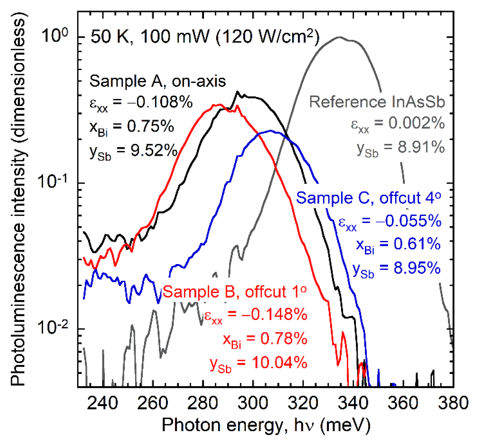
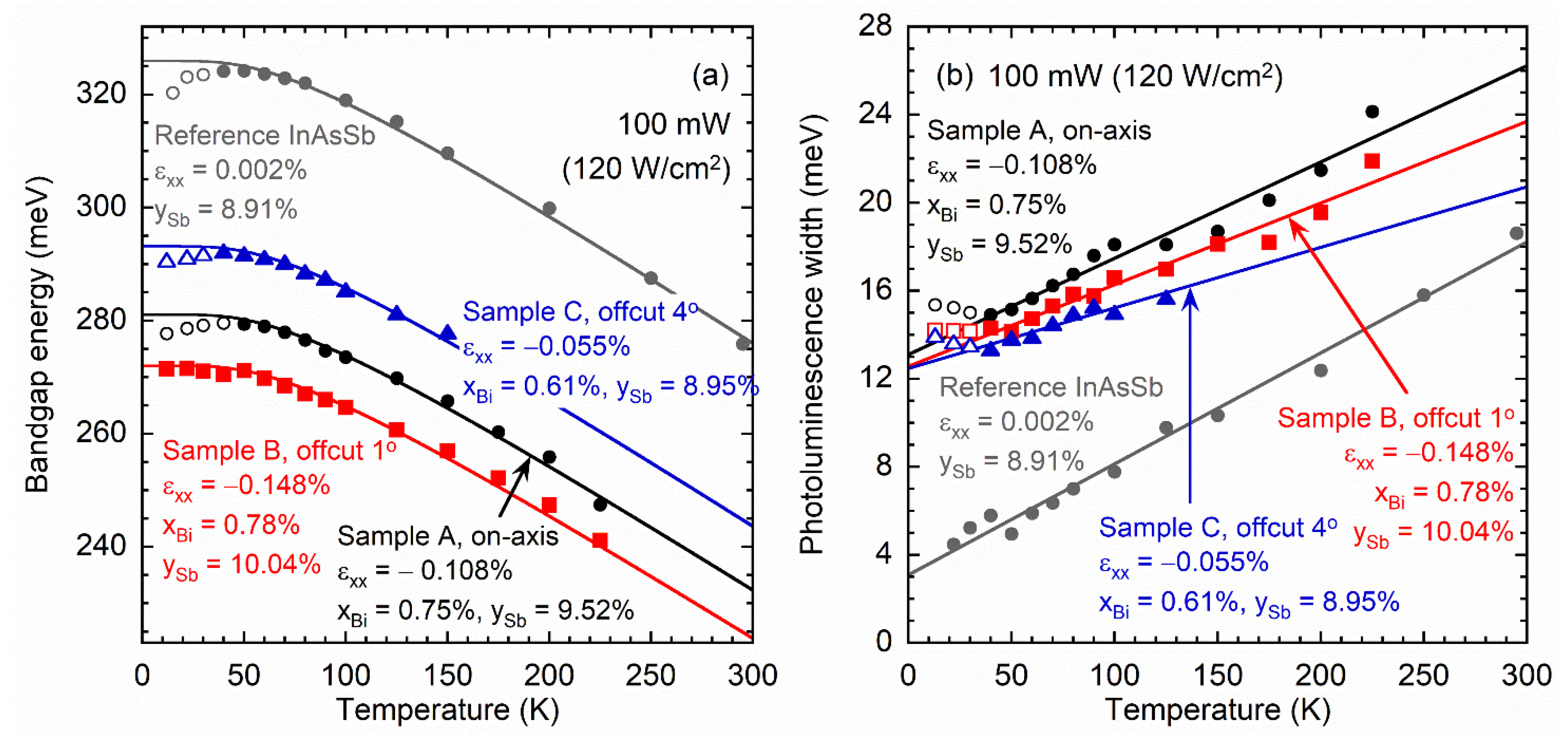
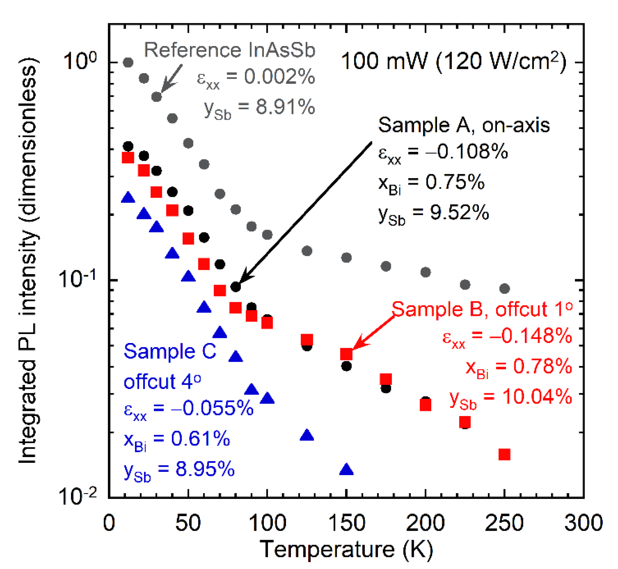
3.4. Photoluminescence Spectroscopy Measurements of InAsSbBi Layers

The on-axis and offcut InAsSbBi samples are examined by steady-state photoluminescence spectroscopy. The measurements are performed at temperatures ranging from 12 to 295 K at a constant laser pump power of 100 mW corresponding to an excitation intensity of 120 W/cm2. Selected photoluminescence spectra measured at 50 K are shown in Figure 11. For comparison, a reference 210 nm thick InAsSb sample grown at 430 °C with the same sample structure as shown in Figure 2 and with Sb/In and As/In flux ratios of 0.126 and 1.193, respectively, is also shown. The photoluminescence intensity is normalized to the InAsSb reference sample. The photoluminescence spectra for the three InAsSbBi samples exhibit similar amplitude and an extended low energy tail corresponding to luminescence from sub-bandgap states. This inhomogeneous broadening at 50 K is primarily a result of frozen-in disorder, alloy broadening, and Bi configuration (e.g., pairing or clustering) on the group V sublattice [4,36,37,38].
The average bandgap energy, identified as the first derivative maximum of the measured photoluminescence spectra [2,3,4,39,40] is plotted as a function of temperature in Figure 12. Carrier localization effects [4,38,41,42,43,44] are observed at measurement temperatures below approximately 50 K and are manifested as a reduction in bandgap energy, shown by the open symbols in Figure 12. The reduction in bandgap energy due to carrier localization is a well-known phenomenon in bismide alloys [4,38,41,42,43,44]. No significant difference in the bandgap reduction or inhomogeneous broadening caused by carrier localization is observed between the on-axis and offcut samples. Einstein single-oscillator model [3,4,36,37] fits to the temperature-dependent bandgap energy data are shown as solid lines in Figure 12a. The characteristic temperature T E is fixed at 200.0 K and the coupling parameter S 0 and low-temperature bandgap energy E g ( T = 0 ) is provided in Table 7 for each of the three samples. Additionally listed in Table 7 are the photoluminescence full-width at half-maximum at low temperature, b w , and its temperature-dependent slope, m w [4]. The low-temperature width b w is a measure of the frozen-in inhomogeneous broadening due to alloying Bi [4] and is approximately 13 meV for the three InAsSbBi samples examined here.
The average Bi, Sb, and As mole fractions are ascertained from XRD measurements of lattice constant and steady-state photoluminescence (PL) measurements of bandgap energy. The InAsSbBi bandgap bowing model [4] and Vegard’s law [31] shown in Equation (3) are solved to determine the average Bi, Sb, and As mole fractions, listed in Table 6. The combined PL and XRD measurements specify an average Bi mole fraction of 0.71% for sample A, 0.82% for sample B, and 0.57% for sample C.
The integrated photoluminescence intensity as a function of temperature is shown in Figure 13, and is normalized to the low-temperature integrated intensity of the 210 nm thick InAsSb reference sample grown at 430 °C. The photoluminescence intensity exhibits a double exponential decrease as temperature increases that is initially steep with characteristic energy of 3 to 4 meV for temperatures below 90 K and that flattens out at temperatures above 90 K with characteristic slopes ranging from 6 meV for InAsSbBi sample C to 24 meV for the reference InAsSb sample.

4. Discussion

The group-V mole fractions from the two measurement methods, TEM + XRD and PL + XRD, are averaged and reported in Table 8. The group-V incorporation coefficients, defined as the ratio of mole fraction to incident V/In flux ratio, are also reported in Table 8. The corresponding mole fraction and incorporation coefficient uncertainties are given by the square root of the sum of the variances from each measurement method. The average Bi mole fractions measured by the TEM + XRD method agree with those measured by the PL + XRD method to within +0.09/-0.06% for the three InAsSbBi samples. The Bi incorporation coefficients range from 12.1% to 14.9% and indicate that only a small portion of the incident Bi flux incorporates in the InAsSbBi layer for growth at 400 °C. In contrast, the Sb incorporation ranges from 79.3% to 85.2%, and the As incorporation is near unity at 97.9% to 99.3%.
Small As overpressures of about 1% are used during the growth of InAsSbBi to assist Bi incorporation [4,16]. Furthermore, the excess As that desorbs from the surface is observed to assist in the desorption of excess Bi [16,24]. However, in all the three samples, some of excess Bi accumulates on the surface and segregates, diffuses, and coalesces to form macroscopic droplets resulting in rough, feature covered surfaces [16]. With an average Bi droplet accumulation coefficient of 13.5%, the results indicate that approximately 72.3% of the incident Bi flux desorbs from the growth surface. These surface droplet features are the primary cause of broadening in the measured X-ray diffraction layer peaks. Transmission electron microscopy images and photoluminescence measurements confirm that the X-ray broadening is not due to large vertical or lateral composition variation, but rather scattering by surface droplets, as the composition non-uniformity measured by these methods is insufficient to result in the observed broadening in the XRD simulations.
The X-ray diffraction, transmission electron microscopy, and photoluminescence spectroscopy measurements indicate that the average Bi incorporation in the 400 °C grown InAsSbBi samples does not vary systematically with the magnitude of the GaSb substrate offcut angle. Bright-field and high-angle annular dark-field TEM images show that all three InAsSbBi layers are free of extended defects such as dislocations or grain boundaries and exhibit sharp, atomically smooth interfaces with the AlSb barrier layers.
The RMS roughness of the 5 µm square AFM images decreases with offcut angle from 0.90 to 0.40 nm. Additionally, on-axis sample A exhibits a rough texture with islands about 10 nm in peak-to-peak height, while offcut samples B and C show smooth surface texture characteristic of step flow growth. A similar reduction in surface roughness with substrate misorientation is observed in the AlGaAs material system [45]. The substrate offcut introduces of a uniform array of monoatomic step edges aligned in the [ 0 1 ¯ 1 ] direction, with the distance between step edges decreasing as offcut angle increases. Kinetic roughening is known to occur during the MBE growth of III-V alloys on (100) on-axis substrates where the distance between step edges is greater than the diffusion length of adsorbed group-III atoms. The step edges serve as sites for adsorbed In atoms to diffuse to and incorporate, thereby suppressing the formation of islands and hillocks present on sample A due to kinetic roughening [46,47] on the sub-micron scale.
Anisotropic droplet features aligned in the [ 0 1 ¯ 1 ] direction are observed on the 1° offcut sample B and to a lesser extent on the 4° offcut sample C. In contrast, the droplet features are roughly isotropic on the on-axis sample A. Two-dimensional Fourier transform analysis of the AFM images in Figure 5 confirms increased spectral power in the [ 011 ] direction corresponding to features aligned in the [ 0 1 ¯ 1 ] direction for the 1° offcut sample B. The spectral power is approximately equal in both the [ 011 ] and [ 0 1 ¯ 1 ] directions for the on-axis sample A confirming the isotropy of these droplet features. The steps formed due to the wafer offcut provide possible nucleation sites for droplet formation. The proximity of the step edges is characterized by large number of nearest neighbors for the arriving atoms to coalesce and form islands at each step [48]. The Schwoebel potential barrier [49] at the step edges can significantly impede the surface diffusion of adatoms between the step surfaces. Hence, preferential diffusion along the step edges is possible resulting in anisotropic features on the surface. The reduced anisotropy of the droplets on 4° offcut sample C with respect to 1° offcut sample B is likely due to the smaller Sb/In flux ratio utilized during growth rather than the degree of offcut. This suggests that the presence of excess unincorporated Sb on the growth surface may aid the preferential diffusion and alignment of the Bi-rich droplet features in the [ 0 1 ¯ 1 ] direction.
The results suggest that the substrate offcut primarily influences growth kinetics on the scale of the In and Bi diffusion lengths and reduces RMS roughness on sub-micron scales. The driving force for droplet formation is the low solid solubility [50] of Bi in the InAs host material and its tendency to accumulate in a surface layer based on the excess unincorporated group-V fluxes [24], which does not depend on substrate offcut angle. Therefore, the substrate offcut does not significantly influence the droplet statistics including density, diameter, height, and volume per unit area.
Lateral composition modulation is manifested as nanocolumns of Bi-rich and Bi-deficient regions extending in the [100] growth direction. Phase separation of Bi-rich columns occurs during the early stages of growth and becomes more pronounced as the growth proceeds. The phase separation depends on the diffusivity of the adsorbed atoms, and hence kinetic factors such as growth temperature influence these nanocolumns. In this work, the growth temperature is held constant at 400 °C and hence the diffusivity of Bi is mainly influenced by the offcut angle magnitude. The 1° offcut sample B exhibits marginally reduced lateral variation in the Bi mole fraction with a standard deviation of uncertainty 0.011% compared to 0.020% and 0.014% for the on-axis sample A and 4° offcut sample C, respectively. The accumulation of excess Bi in droplets aligned in the [ 0 1 ¯ 1 ] direction for sample B may contribute to improved Bi mole fraction uniformity in the InAsSbBi layer in the [ 011 ] direction.
The photoluminescence width at low temperature is a measure of the inhomogeneous broadening introduced by incorporation of Bi. This includes the effects of both the composition modulation observed in TEM images and Bi pairing or clustering on adjacent group-V sublattice sites which modifies the bandgap energy and introduces local strain [38,42]. Previous studies [4] of InAsSbBi grown at temperatures of 400 to 430 °C indicate this inhomogeneous broadening is primarily due to the configuration-dependent incorporation of Bi rather than lateral or vertical composition modulation. The low temperature PL width is approximately constant for the on-axis and offcut InAsSbBi samples examined in this work, suggesting that the presence of a uniform array of step edges in the offcut samples does not significantly impact Bi pairing or clustering on the group-V sublattice.
The integrated photoluminescence intensity measurements in Figure 13 are performed at a moderately high excitation density around 1024 s−1cm−3 (120 W/cm−2) to provide measurable photoluminescence from all samples over a wide range of temperatures. The predominant trends in integrated photoluminescence intensity are the presence of distinct low and high temperature characteristic slopes and a significant decrease in intensity with temperature. In these narrow bandgap materials, the opposing temperature trends of increasing radiative lifetime τ r a d and decreasing non-radiative lifetime results in a total carrier recombination lifetime that is on the order of 10 ns and weakly dependent on temperature. As such, the photoexcited carrier density n is weakly temperature-dependent and in the order of 1016 cm−3. Since the radiative coefficient B , defined as τ r a d = 1 / B n , rapidly decreases with temperature with power law of approximately −2 [51] and the carrier density is weakly dependent on temperature, the photoluminescence intensity markedly decreases with temperature at all temperatures. At around 90 K, where the characteristic slope flattens out, the carrier recombination changes from radiatively dominated at low temperature to nonradiative dominated at high temperature. Furthermore, in the low-temperature region, the carrier density increases slowly with temperature, as is always the case when radiative recombination is the dominant loss mechanism, and in the high-temperature region, the carrier density slowly decreases with temperature, as the nonradiative recombination loss dominates. Therefore, the high temperature region is particularly sensitive to the magnitude of Shockley–Read–Hall nonradiative recombination. The nonradiative Auger recombination is a much smaller loss at these carrier densities and is weakly temperature dependent, and is not considered in the analysis.
A steeper slope (smaller characteristic energy) in the high-temperature region indicates a more rapid decrease in radiative recombination with temperature that is a result of a smaller nonradiative lifetime and a larger radiative lifetime, which, respectively result from a larger density of Shockley–Read–Hall recombination centers and a smaller photoexcited carrier density. The increase in recombination centers is attributed to a larger density of localized states that arise from alloy disorder on the group-V sublattice and Bi clustering on adjacent group-V lattice sites [52,53]. Bi clustering is observed in other III-V-bismide alloys including GaAsBi [52,54] and InPBi [55], among others, and results in local strain and modification of the bulk band structure due to the valence band anti-crossing interaction [56] and introduction of localized states [38].
These results indicate that the bismuth alloys contain a larger density of localized states that act as recombination centers and that within the InAsSbBi samples, the density is largest for the 4° offcut growth. No significant difference is observed between the on-axis and 1° offcut growth. The Sb/In flux ratio may have impacted the 4° offcut growth as it was reduced from 0.120 to 0.105, decreasing the total group V/In flux ratio from 1.081 to 1.066.

5. Conclusions

The molecular beam epitaxy growth of InAsSbBi on (100) on-axis, (100) 1° to [011], and (100) 4° to [011] GaSb substrates is investigated. Substrate offcut is not observed to significantly impact the incorporation of the Bi, Sb, and As or the manner that the Bi atoms incorporate in regard to Bi pairing or clustering on adjacent group-V sublattice sites, as the low-temperature photoluminescence intensity and line width is not observed to significantly change with offcut. The reduction in the high-temperature photoluminescence intensity from the 4° offcut sample indicates the presence of a larger number of nonradiative recombination centers that may be a result of the smaller Sb flux used. Transmission electron microscopy images indicate pseudomorphic, high-quality, defect free InAsSbBi layers with sharp interfaces for each substrate offcut. Substrate offcut reduces the surface roughness of the sample layers with a slight reduction in the lateral variation of the Bi mole fraction. Droplet features are observed on all sample surfaces. Of the incident fluxes, 9% to 19% of the Bi flux and 3.5% to 4.6% of the In flux accumulates on the surface and coalesces into droplet features. The surface droplets are isotropic on the on-axis sample and are elongated along the [ 0 1 ¯ 1 ] step edges on the 1° and 4° offcut samples. The average droplet diameter, height, and surface coverage do not vary significantly with substrate offcut.

Author Contributions

Conceptualization, R.R.K. and S.T.S.; methodology, R.R.K., S.T.S., and M.S.M.; software, R.R.K.; validation, S.T.S. and M.S.M.; formal analysis, R.R.K., S.T.S., and S.R.J.; investigation, R.R.K., S.T.S., and S.R.J.; resources, S.R.J.; data curation, R.R.K., S.T.S., and M.S.M.; writing—original draft preparation, R.R.K.; writing—review and editing, S.T.S. and S.R.J.; visualization, R.R.K. and S.T.S.; supervision, S.R.J.; project administration, S.R.J.; funding acquisition, S.R.J. All authors have read and agreed to the published version of the manuscript.

Funding

This research was funded by Air Force Research Laboratory under agreement number FA9453-19-2-0004. The U.S. Government is authorized to reproduce and distribute reprints for Governmental purposes notwithstanding any copyright notation thereon.

Data Availability Statement

The data that support the findings of this study are available from the corresponding author upon reasonable request.

Acknowledgments

The authors gratefully acknowledge the use of facilities in the Eyring Materials Center at Arizona State University.

Conflicts of Interest

The authors declare no conflict of interest. The funders had no role in the design of the study; in the collection, analyses, or interpretation of data; in the writing of the manuscript, or in the decision to publish the results.

Disclaimer

The views and conclusions contained herein are those of the authors and should not be interpreted as necessarily representing the official policies or endorsements, either expressed or implied, of Air Force Research Laboratory or the U.S. Government.

References

  1. Downs, C.; Vandervelde, T.E. Progress in Infrared Photodetectors Since 2000. Sensors 2013, 13, 5054–5098. [Google Scholar] [CrossRef] [PubMed]
  2. Webster, P.T.; Shalindar, A.J.; Riordan, N.A.; Gogineni, C.; Liang, H.; Sharma, A.R.; Johnson, S.R. Optical properties of InAsBi and optimal designs of lattice-matched and strain-balanced III-V semiconductor superlattices. J. Appl. Phys. 2016, 119, 225701. [Google Scholar] [CrossRef]
  3. Webster, P.T.; Riordan, N.A.; Liu, S.; Steenbergen, E.H.; Synowicki, R.A.; Zhang, Y.-H.; Johnson, S.R. Measurement of InAsSb bandgap energy and InAs/InAsSb band edge positions using spectroscopic ellipsometry and photoluminescence spectroscopy. J. Appl. Phys. 2015, 118, 245706. [Google Scholar] [CrossRef] [Green Version]
  4. Schaefer, S.T.; Kosireddy, R.R.; Webster, P.T.; Johnson, S.R. Molecular beam epitaxy growth and optical properties of InAsSbBi. J. Appl. Phys. 2019, 126, 083101. [Google Scholar] [CrossRef]
  5. Tisch, U.; Finkman, E.; Salzman, J. The anomalous bandgap bowing in GaAsN. Appl. Phys. Lett. 2002, 81, 463–465. [Google Scholar] [CrossRef]
  6. Guina, M.; Wang, S.M.; Aho, A. Molecular Beam Epitaxy of Dilute Nitride Optoelectronic Devices. In Molecular Beam Epitaxy: From Research to Mass Production, 2nd ed.; Henini, M., Ed.; Elsevier: Amsterdam, The Netherlands, 2018; p. 73. [Google Scholar]
  7. Shan, W.; Walukiewicz, W.; Ager, I.J.W.; Haller, E.E.; Geisz, J.F.; Friedman, D.J.; Olson, J.M.; Kurtz, S.R. Band Anticrossing in GaInNAs Alloys. Phys. Rev. Lett. 1999, 82, 1221–1224. [Google Scholar] [CrossRef]
  8. Shan, W.; Walukiewicz, W.; Wu, J.; Yu, K.M.; Ager, J.W., III; Li, S.X.; Haller, E.E.; Geisz, J.F.; Friedman, D.J.; Kurtz, S.R. Band-gap bowing effects in BxGa1−xAs alloys. J. Appl. Phys. 2003, 93, 2696. [Google Scholar] [CrossRef] [Green Version]
  9. Alberi, K.; Wu, J.; Walukiewicz, W.; Yu, K.M.; Dubon, O.D.; Watkins, S.P.; Wang, C.X.; Liu, X.; Cho, Y.-J.; Furdyna, J. Va-lence-band anticrossing in mismatched III–V semiconductor alloys. Phys. Rev. B 2007, 75, 045203. [Google Scholar] [CrossRef]
  10. Fluegel, B.; Mascarenhas, A.; Ptak, A.J.; Tixier, S.; Young, E.C.; Tiedje, T. E+ transition in GaAs1−xNx and GaAs1−xBix due to isoelectronic-impurity-induced perturbation of the conduction band. Phys. Rev. B 2007, 76, 155209. [Google Scholar] [CrossRef]
  11. Tixier, S.; Adamcyk, M.; Tiedje, T.; Francoeur, S.; Mascarenhas, A.; Wei, P.; Schiettekatte, F. Molecular beam epitaxy growth of GaAs1-xBix. Appl. Phys. Lett. 2003, 82, 2245. [Google Scholar] [CrossRef]
  12. Francoeur, S.; Seong, M.-J.; Mascarenhas, A.; Tixier, S.; Adamcyk, M.; Tiedje, T. Band gap of GaAs1−xBix, 0 < x < 3.6%. Appl. Phys. Lett. 2003, 82, 3874. [Google Scholar] [CrossRef]
  13. Batool, Z.; Chatterjee, S.; Chernikov, A.; Duzik, A.; Fritz, R.; Gogineni, C.; Hild, K.; Hosea, T.J.C.; Imhof, S.; Johnson, S.R.; et al. Bismuth-containing III–V semiconductors: Epitaxial growth and physical properties. In Molecular Beam Epitaxy: From Research to Mass Production, 1st ed.; Henini, M., Ed.; Elsevier: Amsterdam, The Netherlands, 2013; pp. 139–158. [Google Scholar]
  14. Shalindar, A.J.; Webster, P.T.; Schaefer, S.T.; Johnson, S.R. InAsBi Materials. In Molecular Beam Epitaxy: From Research to Mass Production, 2nd ed.; Henini, M., Ed.; Elsevier: Amsterdam, The Netherlands, 2018; p. 181. [Google Scholar]
  15. Fluegel, B.; Francoeur, S.; Mascarenhas, A.; Tixier, S.; Young, E.C.; Tiedje, T. Giant Spin-Orbit Bowing in GaAs1-xBix. Phys. Rev. Lett. 2006, 97, 067205. [Google Scholar] [CrossRef] [PubMed]
  16. Kosireddy, R.R.; Schaefer, S.T.; Shalindar, A.J.; Johnson, S.R. Microstructure and surface morphology of InAsSbBi grown by molecular beam epitaxy. J. Appl. Phys. 2019, 126, 095108. [Google Scholar] [CrossRef]
  17. Kosireddy, R.R.; Schaefer, S.T.; Shalindar, A.J.; Webster, P.T.; Johnson, S.R. Examination of the Structural Quality of InAsSbBi Epilayers using Cross Section Transmission Electron Microscopy. Microsc. Microanal. 2018, 24, 36–37. [Google Scholar] [CrossRef] [Green Version]
  18. Luna, E.; Wu, M.; Puustinen, J.; Guina, M.; Trampert, A. Spontaneous formation of nanostructures by surface spinodal de-composition in GaAs1−x Bix epilayers. J. Appl. Phys. 2015, 117, 185302. [Google Scholar] [CrossRef]
  19. Wu, M.; Hanke, M.; Luna, E.; Puustinen, J.; Guina, M.; Trampert, A. Detecting lateral composition modulation in dilute Ga(As,Bi) epilayers. Nanotechnology 2015, 26, 425701. [Google Scholar] [CrossRef] [PubMed]
  20. Luna, E.; Puustinen, J.; Wu, M.; Hilska, J.; Guina, M.; Trampert, A. The Role of Epitaxial Strain on the Spontaneous Formation of Bi-Rich Nanostructures in Ga(As,Bi) Epilayers and Quantum Wells. Nanosci. Nanotechnol. Lett. 2017, 9, 1132–1138. [Google Scholar] [CrossRef]
  21. Luna, E.; Delorme, O.; Cerutti, L.; Tournié, E.; Rodriguez, J.-B.; Trampert, A. Microstructure and interface analysis of emerging Ga(Sb,Bi) epilayers and Ga(Sb,Bi)/GaSb quantum wells for optoelectronic applications. Appl. Phys. Lett. 2018, 112, 151905. [Google Scholar] [CrossRef]
  22. Duzik, A.; Millunchick, J.M. Surface morphology and Bi incorporation in GaSbBi(As)/GaSb films. J. Cryst. Growth 2014, 390, 5. [Google Scholar] [CrossRef]
  23. Lu, J.; Webster, P.T.; Liu, S.; Zhang, Y.H.; Johnson, S.R.; Smith, D.J. Investigation of MBE-grown InAs1-xBix alloys and Bi-mediated type-II superlattices by transmission electron microscopy. J. Cryst. Growth 2015, 425, 250. [Google Scholar] [CrossRef] [Green Version]
  24. Schaefer, S.T.; Milosavljevic, M.S.; Kosireddy, R.R.; Johnson, S.R. Kinetic model for molecular beam epitaxy growth of InAsSbBi alloys. J. Appl. Phys. 2021, 129, 035303. [Google Scholar] [CrossRef]
  25. Wafer Technology Ltd. 34 Maryland Road, Milton Keynes, MK15 8HJ, UK. Available online: http://wafertech.co.uk/ (accessed on 14 April 2021).
  26. X’pert Epitaxy Software; Panalytical B.V.: Almelo, The Netherlands, 2007.
  27. Matthews, J.; Blakeslee, A. Defects in epitaxial multilayers. J. Cryst. Growth 1974, 27, 118–125. [Google Scholar] [CrossRef]
  28. Nečas, D.; Klapetek, P. Gwyddion: An open-source software for SPM data analysis. Cent. Eur. J. Phys. 2012, 10, 181–188. [Google Scholar] [CrossRef]
  29. Bithell, E.G.; Stobbs, W.M. Composition determination in the GaAs/(Al, Ga)As system using contrast in dark-field transmission electron microscope images. Philos. Mag. A 1989, 60, 39–62. [Google Scholar] [CrossRef]
  30. Doyle, P.A.; Turner, P.S. Relativistic Hartree–Fock X-ray and electron scattering factors. Acta Crystallogr. Sect. A 1968, 24, 390. [Google Scholar] [CrossRef]
  31. Vegard, L. Die Konstitution der Mischkristalle und die Raumfüllung der Atome. Z. Phys. 1921, 5, 17–26. [Google Scholar] [CrossRef]
  32. Vurgaftman, I.; Meyer, J.R.; Ram-Mohan, L.R. Band parameters for III–V compound semiconductors and their alloys. J. Appl. Phys. 2001, 89, 5815–5875. [Google Scholar] [CrossRef] [Green Version]
  33. Shalindar, A.J.; Webster, P.T.; Wilkens, B.J.; Alford, T.L.; Johnson, S.R. Measurement of InAsBi mole fraction and InBi lattice constant using Rutherford backscattering spectrometry and X-ray diffraction. J. Appl. Phys. 2016, 120, 145704. [Google Scholar] [CrossRef]
  34. Pennycook, S.J.; Chisholm, M.F.; Lupini, A.R.; Varela, M.; Borisevich, A.; Oxley, M.; Luo, W.D.; Van Benthem, K.; Oh, S.-H.; Sales, D.L.; et al. Aberration-corrected scanning transmission electron microscopy: From atomic imaging and analysis to solving energy problems. Philos. Trans. R. Soc. A Math. Phys. Eng. Sci. 2009, 367, 3709–3733. [Google Scholar] [CrossRef]
  35. Smith, D.J.; Lu, J.; Aoki, T.; McCartney, M.R.; Zhang, Y.-H. Observation of compound semiconductors and heterovalent interfaces using aberration-corrected scanning transmission electron microscopy. J. Mater. Res. 2017, 32, 921–927. [Google Scholar] [CrossRef]
  36. Johnson, S.R.; Tiedje, T. Temperature dependence of the Urbach edge in GaAs. J. Appl. Phys. 1995, 78, 5609–5613. [Google Scholar] [CrossRef] [Green Version]
  37. Viña, L.; Logothetidis, S.; Cardona, M. Temperature dependence of the dielectric function of germanium. Phys. Rev. B 1984, 30, 1979–1991. [Google Scholar] [CrossRef]
  38. Bannow, L.C.; Rubel, O.; Badescu, S.C.; Rosenow, P.; Hader, J.; Moloney, J.V.; Tonner, R.; Koch, S.W. Configuration de-pendence of band gap narrowing and localization in dilute GaAs1-xBix alloys. Phys. Rev. B 2016, 93, 205202. [Google Scholar] [CrossRef] [Green Version]
  39. Webster, P.T.; Riordan, N.A.; Liu, S.; Steenbergen, E.H.; Synowicki, R.A.; Zhang, Y.-H.; Johnson, S.R. Absorption properties of type-II InAs/InAsSb superlattices measured by spectroscopic ellipsometry. Appl. Phys. Lett. 2015, 106, 061907. [Google Scholar] [CrossRef] [Green Version]
  40. Souri, D.; Tahan, Z.E. A new method for the determination of optical band gap and the nature of optical transitions in semiconductors. Appl. Phys. A 2015, 119, 273–279. [Google Scholar] [CrossRef]
  41. Christian, T.M.; Alberi, K.; Beaton, D.A.; Fluegel, B.; Mascarenhas, A. Spectrally resolved localized states in GaAs1−xBix. Jpn. J. Appl. Phys. 2017, 56, 35801. [Google Scholar] [CrossRef]
  42. Chen, X.; Shen, W.; Liang, D.; Quhe, R.; Wang, S.; Guan, P.; Lu, P. Effects of Bi on band gap bowing in InP1-xBix alloys. Opt. Mater. Express 2018, 8, 1184–1192. [Google Scholar] [CrossRef]
  43. Mohmad, A.R.; Bastiman, F.; Hunter, C.J.; Richards, R.; Sweeney, S.; Ng, J.S.; David, J.P.R.; Majlis, B.Y. Localization effects and band gap of GaAsBi alloys. Phys. Status Solidi B 2014, 251, 1276–1281. [Google Scholar] [CrossRef]
  44. Mohmad, A.R.; Bastiman, F.; Hunter, C.J.; Ng, J.S.; Sweeney, S.J.; David, J.P.R. The effect of Bi composition to the optical quality of GaAs1−xBix. Appl. Phys. Lett. 2011, 99, 42107. [Google Scholar] [CrossRef] [Green Version]
  45. Tsui, R.K.; Curless, J.A.; Kramer, G.D.; Peffley, M.S.; Rode, D.L. Effects of substrate misorientation on the properties of (Al, Ga)As grown by molecular beam epitaxy. J. Appl. Phys. 1985, 58, 2570–2572. [Google Scholar] [CrossRef]
  46. Rode, D.L.; Wagner, W.R.; Schumaker, N.E. Singular instabilities on LPE GaAs, CVD Si, and MBE InP growth surfaces. Appl. Phys. Lett. 1977, 30, 75–78. [Google Scholar] [CrossRef]
  47. Orr, B.G.; Johnson, M.D.; Orme, C.; Sudijono, J.; Hunt, A.W. The surface evolution and kinetic roughening during ho-moepitaxy of GaAs (001). Solid-State Electron. 1994, 37, 1057. [Google Scholar] [CrossRef] [Green Version]
  48. Tersoff, J. Step Energies and Roughening of Strained Layers. Phys. Rev. Lett. 1995, 74, 4962. [Google Scholar] [CrossRef]
  49. Schwoebel, R.L.; Shipsey, E.J. Step Motion on Crystal Surfaces. J. Appl. Phys. 1966, 37, 3682–3686. [Google Scholar] [CrossRef]
  50. Ma, K.; Fang, Z.; Cohen, R.; Stringfellow, G. OMVPE growth and characterization of Bi-containing III–V alloys. J. Cryst. Growth 1991, 107, 416–421. [Google Scholar] [CrossRef]
  51. Johnson, S.R.; Ding, D.; Wang, J.-B.; Yu, S.-Q.; Zhang, Y.-H. Excitation dependent photoluminescence measurements of the nonradiative lifetime and quantum efficiency in GaAs. J. Vac. Sci. Technol. B Microelectron. Nanometer Struct. 2007, 25, 1077. [Google Scholar] [CrossRef]
  52. Imhof, S.; Thränhardt, A.; Chernikov, A.; Koch, M.; Köster, N.S.; Kolata, K.; Chatterjee, S.; Koch, S.W.; Lu, X.; Johnson, S.R.; et al. Clustering effects in Ga(AsBi). Appl. Phys. Lett. 2010, 96, 131115. [Google Scholar] [CrossRef]
  53. Gogineni, C.; Riordan, N.A.; Johnson, S.R.; Lu, X.; Tiedje, T. Disorder and the Urbach edge in dilute bismide GaAsBi. Appl. Phys. Lett. 2013, 103, 041110. [Google Scholar] [CrossRef]
  54. Ciatto, G.; Young, E.C.; Glas, F.; Chen, J.; Mori, R.A.; Tiedje, T. Spatial correlation between Bi atoms in dilute GaAs1-xBix: From random distribution to Bi pairing and clustering. Phys. Rev. B 2008, 78, 035325. [Google Scholar] [CrossRef]
  55. Wang, K.; Gu, Y.; Zhou, H.F.; Zhang, L.Y.; Kang, C.Z.; Wu, M.J.; Pan, W.W.; Lu, P.F.; Gong, Q.; Wang, S.M. InPBi Single Crystals Grown by Molecular Beam Epitaxy. Sci. Rep. 2014, 4, 5449. [Google Scholar] [CrossRef] [Green Version]
  56. Hader, J.; Badescu, S.C.; Bannow, L.C.; Moloney, J.V.; Johnson, S.R.; Koch, S.W. Extended band anti-crossing model for dilute bismides. Appl. Phys. Lett. 2018, 112, 062103. [Google Scholar] [CrossRef]
Figure 1. Nominal growth cross-section of the InAsSbBi samples examined. The substrate temperature profile is shown at left. The layers consist of a 500 nm GaSb buffer, a 10 nm InAs/10 nm AlSb partially strain balanced barrier, the InAsSbBi active region, and a terminating 10 nm AlSb/10 nm InAs barrier/cap layer.
Photonics 08 00215 g001
Figure 2. Substrate surfaces on-axis without step edges (left schematic) and offcut with smooth step edges in the [ 01 1 ¯ ] direction (right schematic).
Photonics 08 00215 g002
Figure 3. Coupled ω 2 θ scans from the (400) reflection in the [ 0 1 ¯ 1 ] direction (red) and [ 01 1 ¯ ] direction (blue) and the dynamical simulation (black) for InAsSbBi samples A through C, shown in (ac), respectively. The GaSb substrate peak, compressive InAsSbBi layer peak, and the tensile GaAsSb buffer peak are shown. The average mole fractions reported in Table 8 are indicated on the figure along with the in-plane biaxial strain. The Bi/In, As/In, and Sb/In flux ratios are 0.05, 0.91, and 0.10 to 0.12 for all the samples, respectively.
Photonics 08 00215 g003
Figure 4. Nomarski optical measurements of the surface morphology of bulk InAsSbBi samples A through C, shown in (ac), respectively. Image dimensions are 100 µm by 75 µm. The Bi/In, As/In, and Sb/In flux ratios and substrate orientation are shown for each sample.
Photonics 08 00215 g004
Figure 5. Atomic force microscopy images of the surface morphology of bulk InAsSbBi sample A (a,b), sample B (c,d), and sample C (e,f). Images’ dimensions are 100 µm by 100 µm on the left and 5 µm by 5 µm on the right. The root mean square (RMS) roughness ranges from 49 to 36 nm over the 100 µm square area and 0.90 to 0.40 nm over the 5 µm square area. The Bi/In, As/In, and Sb/In flux ratios and substrate orientation are shown for each sample.
Photonics 08 00215 g005
Figure 6. Bright field cross-section TEM images in the [ 01 1 ¯ ] projection showing the overall microstructure of InAsSbBi samples A through C, in (ac), respectively. Contrast modulation with period of approximately 30 nm is observed perpendicular to the growth plane in (a) and (c). The Bi/In, As/In, and Sb/In flux ratios and substrate orientation are shown.
Photonics 08 00215 g006
Figure 7. Chemically sensitive (200) dark-field TEM images in the [ 01 1 ¯ ] projection from InAsSbBi samples A through C in (ac), respectively. Line scans of the image intensity from the regions marked as rectangles parallel to the layer interface are shown.
Photonics 08 00215 g007
Figure 8. Lateral intensity profiles (a) and Bi mole fraction profiles (b) obtained from chemically sensitive 200 dark-field images of InAsSbBi samples A through C, with the significant growth conditions shown for each.
Photonics 08 00215 g008
Figure 9. High-angle annular dark-field scanning TEM images in the [ 01 1 ¯ ] projection showing the overall microstructure of InAsSbBi samples A, B, and C, in (a–c), respectively. Line scans of the image intensity from the regions marked by the rectangles parallel to the layer interface are shown for sample A, B, and C in (df), respectively. Contrast modulations perpendicular to the growth direction in (a) and (c) show composition inhomogeneity with a modulation period of approximately 30 nm. The Bi/In, As/In, and Sb/In flux ratios and substrate orientation are shown for all samples.
Photonics 08 00215 g009
Figure 10. Atomic resolution high-angle-annular dark-field scanning TEM images in the [01 1 ¯ ] projection showing the top and bottom interfaces of InAsSbBi samples A, B, and CI in (af), respectively. Atomic steps are observed and marked in (d) and (f). The Bi/In, As/In, and Sb/In flux ratios and substrate orientation are shown.
Photonics 08 00215 g010
Figure 11. Photoluminescence intensity measured at 50 K as a function of photon energy for InAsSbBi sample A (black line), sample B (red line), sample C (blue line), and reference InAsSb (grey line). All measurements are performed at a constant laser pump power of 100 mW corresponding to an excitation intensity of 120 W/cm2.
Photonics 08 00215 g011
Figure 12. Bandgap energy (a) and photoluminescence width (b) vs. temperature for InAsSbBi sample A (black circles), sample B (red squares), sample C (blue triangles), and reference InAsSb (grey circles). Einstein’s single-oscillator model fits in (a) and linear fits in (b) are shown as solid lines. Filled symbols are fitted data points while open symbols are not fitted. All measurements are performed at a constant laser pump power of 100 mW corresponding to an excitation intensity of 120 W/cm2.
Photonics 08 00215 g012
Figure 13. Integrated photoluminescence intensity as a function of measurement temperature for InAsSbBi sample A (black circles), sample B (red squares), sample C (blue triangles), and reference InAsSb (grey circles). All measurements are performed at a constant laser pump power of 100 mW corresponding to an excitation intensity of 120 W/cm2.
Photonics 08 00215 g013
Table 1. InAsSbBi sample name, substrate orientation, growth temperature, V/In flux ratios, excess V/In flux ratios, and the presence of surface droplet features.
SampleSubstrate
Orientation
Growth
Temperature
V/In Flux RatiosExcess V/In Flux RatiosSurface
Droplets
Bi/InSb/InAs/InBi/InSb/InAs/In
A(100)400 °C0.0500.1200.9110.0430.0250.014Yes
B(100) 1° to [011]400 °C0.0500.1200.9110.0420.0200.019Yes
C(100) 4° to [011]400 °C0.0500.1050.9110.0440.0150.007Yes
Table 2. Simulated InAsSbBi layer thickness, out-of-plane distortion, lattice constant, and in-plane strain; simulated angular separation of the InAsSbBi and GaSb Bragg angles θ G a S b θ I n A s S b B i and simulated angular separation of the InAsSbBi and GaSb peaks θ G a S b θ S i m u l a t e d ; and measured angular separation of the InAsSbBi and GaSb layer peaks θ G a S b θ P e a k for each of the two measurement directions.
SampleA, (100) on-axisB, (100) 1° to [011]C, (100) 4° to [011]
Simulated thickness (nm)194 ± 1189 ± 1190 ± 1
Out-of-plane distortion ε (%)0.2264 ± 0.00190.3092 ± 0.00190.1148 ± 0.0019
In-plane biaxial strain ε x x (%)−0.1083 ± 0.0009−0.1479 ± 0.0009−0.0550 ± 0.0009
Lattice constant a I n A s S b B i (Å)6.1025 ± 0.00016.1049 ± 0.00016.0993 ± 0.0001
θ G a S b θ I n A s S b B i   (arcsec)273.6 ± 2.3373.6 ± 2.3138.7 ± 2.3
θ G a S b θ S i m u l a t e d (arcsec)270.9375.0129.8
θ G a S b θ P e a k   (arcsec)272.5, 273.2373.9, 375.3129.3, 129.0
Table 3. Root mean square (RMS) surface roughness of samples A through C from atomic force microscopy measurements over surface areas of 100 µm by 100 µm, 5 µm by 5 µm, and 1 µm by 1 µm. The InAsSbBi growth information is provided for each sample.
SampleSubstrate
Orientation
Flux RatiosRMS Roughness (nm)
Bi/InSb/InAs/In100 µm by 100 µm5 µm by 5 µm1 µm by 1 µm
A(100) on-axis0.0500.1200.911490.900.46
B(100) 1° to [011]0.0500.1200.911360.770.52
C(100) 4° to [011]0.0500.1050.911370.440.41
Table 4. Surface droplet density, diameter, height, fraction of surface area covered, volume per unit area, and fraction of incident Bi flux accumulated in droplets determined by Nomarski optical microscopy and atomic force microscopy (AFM) for samples A, B, and C.
SampleA, (100) on-axisB, (100) 1° to [011]C, (100) 4° to [011]
MethodNomarskiAFMNomarskiAFMNomarskiAFM
Density (cm−2)1.8 × 1061.04 × 1062.4 × 1061.19 × 1063.2 × 1061.88 × 106
Diameter (µm)2.62.022.12.171.91.90
Average height (nm)-79.5-68.7-69.6
Surface coverage (%)9.68.18.312.69.112.6
Volume/unit area (nm)-8.6-10.2-10.0
Bi droplet accumulation (%)-18.9-9.2-12.4
In droplet accumulation (%)-3.5-4.6-4.4
Table 5. InAsSbBi unstrained lattice constant a I n A s S b B i , out-of-plane strained lattice constant a I n A s S b B i , scattering angle parameter s , and atomic scattering factors for Al, In, As, Sb, and Bi.
Sample a I n A s S b B i   ( Å ) a I n A s S b B i   ( Å ) s   ( Å 1 ) f A l   ( Å ) f I n   ( Å ) f A s   ( Å ) f S b   ( Å ) f B i   ( Å )
A6.10256.10970.163672.90136.47574.73387.00978.7681
B6.10496.11470.163542.90356.47904.73647.01348.7722
C6.09936.10290.163862.89836.47144.73047.00478.7626
Table 6. InAsSbBi substrate orientation and average group-V mole fractions (%) determined from X-ray diffraction (XRD) and dark-field transmission electron microscopy (TEM + XRD) or photoluminescence spectroscopy (PL + XRD). Total mole fraction uncertainties are provided.
SampleTEM + XRD Mole Fractions (%)PL + XRD Mole Fractions (%)
BiSbAsBiSbAs
A, on-axis0.78 ± 0.0209.47 ± 0.1689.74 ± 0.180.71 ± 0.229.57 ± 0.2889.72 ± 0.50
B, offcut 1°0.73 ± 0.01110.08 ± 0.1489.16 ± 0.150.82 ± 0.2210.00 ± 0.2889.18 ± 0.51
C, offcut 4°0.65 ± 0.0148.91 ± 0.1590.44 ± 0.160.57 ± 0.218.98 ± 0.2890.45 ± 0.49
Table 7. Low-temperature bandgap energy, Einstein single-oscillator model coupling parameter, photoluminescence width parameters, and integrated intensity at 50 K, 100 mW excitation from steady-state photoluminescence spectroscopy measurements.
SampleA, on-axisB, Offcut 1°C, Offcut 4°
Low-temperature bandgap, E g ( T = 0 ) (meV)281.1272.0293.1
Coupling parameter, S 0 (dimensionless)2.6782.6502.721
Photoluminescence width slope, m w (dimensionless)0.5070.4310.319
Photoluminescence width intercept, b w (meV)13.1012.5612.47
Table 8. InAsSbBi substrate orientation, group-V mole fractions (%), and incorporation coefficients (%) averaged across both the TEM + XRD and PL + XRD measurement methods. Total mole fraction and incorporation coefficient uncertainties are provided.
SampleMole Fractions (%)Incorporation Coefficients (%)
BiSbAsBiSbAs
A, on-axis0.75 ± 0.129.52 ± 0.2289.73 ± 0.3414.9 ± 2.479.3 ± 1.898.5 ± 0.4
B, offcut 1°0.78 ± 0.1210.04 ± 0.2189.17 ± 0.3315.5 ± 2.383.7 ± 1.897.9 ± 0.4
C, offcut 4°0.61 ± 0.118.95 ± 0.2290.44 ± 0.3312.1 ± 2.285.2 ± 1.899.3 ± 0.4
Publisher’s Note: MDPI stays neutral with regard to jurisdictional claims in published maps and institutional affiliations.

