1. Introduction
A guided-mode resonance (GMR) device consists of a waveguide layer and grating structure, and incident light can be coupled to the waveguide layer by the grating high diffraction orders. Because of the grating, the propagation wave inside the waveguide layer slowly leaks out of the waveguide guide, and when the incident light wavelength is at the resonance wavelength, the leakage wave interferes with the non-diffraction wave to produce nearly 0% transmittance and 100% reflectivity as a filter response [
1]. This resonance angle is highly sensitive to the refractive index (RI) of material on the grating surface; therefore, the GMR device can be used as a label-free biosensor [
2]. Among the GMR sensor interrogation methods, the phase-based interferometric approach has been proved to have a better detection resolution [
3,
4]. In our previous works, heterodyne interferometry based on an electro-optic modulator was presented [
5] and subsequently, phase-shift interferometry (PSI) based on two liquid-crystal (LC) retardation plates was also proposed [
6]. Our results showed that the phase-detection sensitivity of the RI change on the grating surface of the GMR device can be better than 5000°/RIU. Since the PSI is an image-type detection, it can achieve parallel (multi-channel) sensing and has great potential for high-throughput screening. In this paper, we propose using a digital micromirror device (DMD) to replace the LC device in our previous work to implement the PSI system. The LC device in the PSI needs a calibration process to obtain an accurate analog driving voltage. The DMD-based spatial light modulator (SLM) can display shifting grating patterns to achieve four digital phase-shifting, 0, π/2, π, and 3π/2, without the calibration process. A PSI system implemented by an electrically addressed liquid-crystal-based SLM has been proposed [
7]. Here, the DMD-SLM is proposed to substitute the LC-SLM because the DMD-SLM has a better reflectivity and higher operation speed [
8,
9]. We propose to use the DMD-SLM to facilitate digital phase-shifting in the PSI system using proper micro-mirror patterns without the need for the accurate analog driving voltage in the LC device. We also propose a method to use this DMD-SLM-based PSI system to perform the phase measurement of the GMR device. Besides, because of mature batch-type production technologies, DMD chips have become cost-effective and more attractive for many applications. The diffraction properties of the DMD-SLM are different from the LC-SLM. We will first investigate diffraction patterns of the DMD with different grating patterns and then describe how to utilize the DMD-SLM in the PSI system. Subsequently, fabrication and simulation of the GMR device will be briefly reviewed. Finally, we will demonstrate the measurement results of the phase difference between the
s- and
p-polarization of the GMR sensor using this DMD-based PSI system.
2. DMD Grating and Its Diffraction Pattern
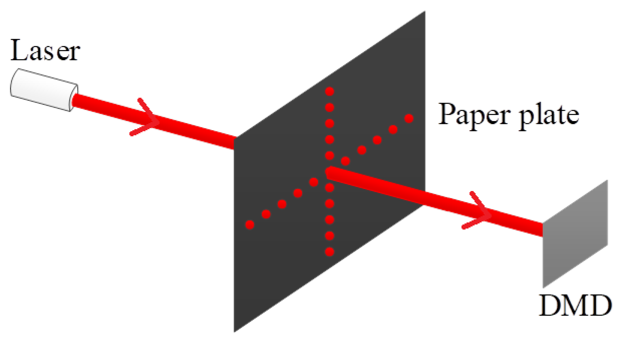
A schematic of the setup for observation of the diffraction patterns of a DMD grating is illustrated in
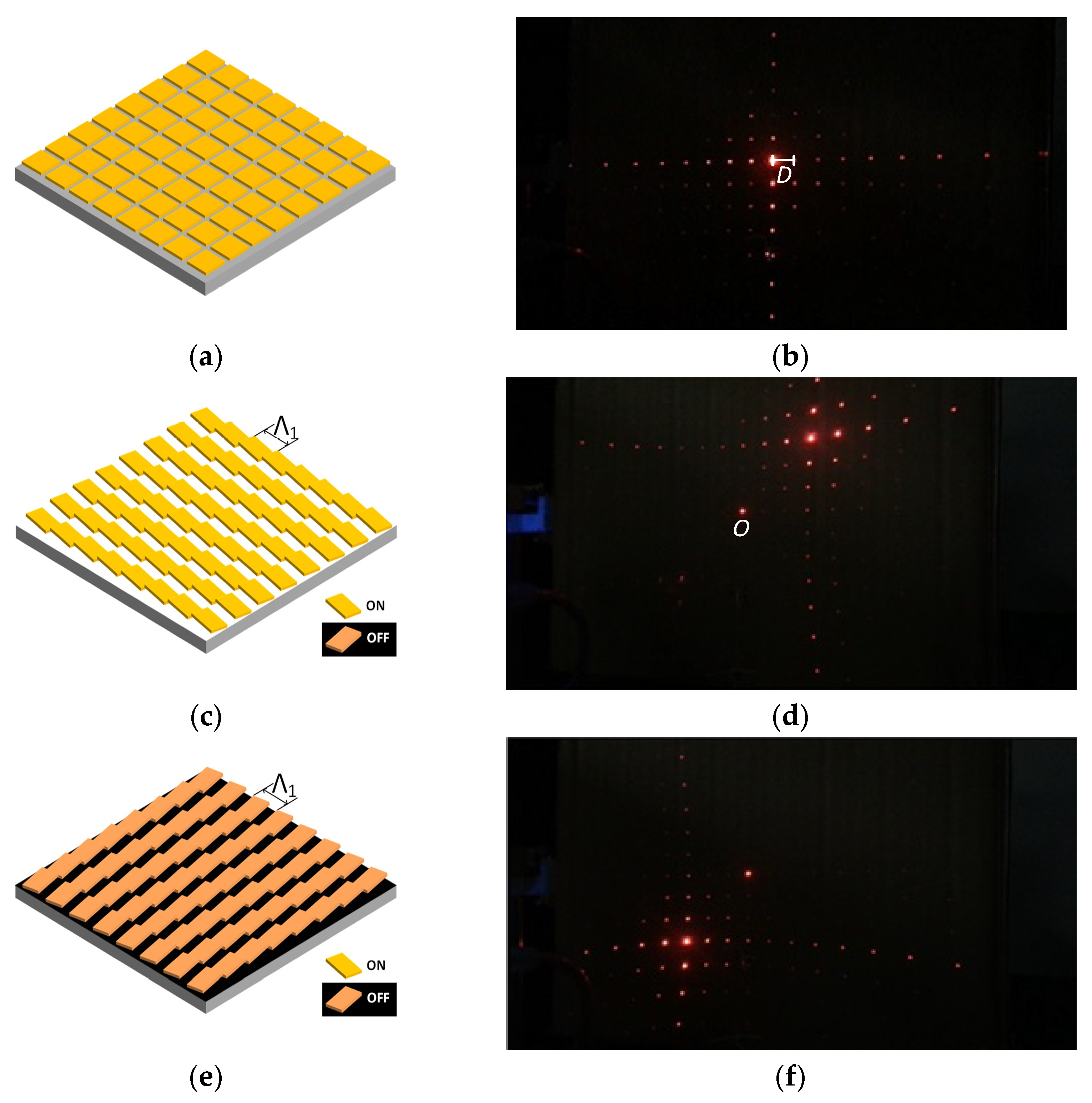
Figure 1. A He-Ne laser with a wavelength of 632.8 nm was normally incident to the DMD surface through a hole in a black-color paper plate that was 1 m away from the DMD surface, and light spots of the reflective diffraction beams could be observed on the paper plate. Because the DMD was a two-dimensional (2D) grating pattern, diffraction spots along the vertical and horizontal directions were expected to be observed. The schematic of all the DMD pixels in the static state (without applying voltage) is as shown in
Figure 2a, in which all micromirrors were parallel to the substrate. The pitch (period) of the 2D gratings is equal to the width of a pixel cell as indicated in
Figure 2a [
10]. Its diffraction spot image is shown in
Figure 2b. Multiple order diffraction light spots were observed, and the zeroth-order light reflected through the hole in the paper plate. The DMD 2D array pixels can be mathematically treated as a convolution of the rectangle (“
rect”) and the comb (“
comb”) functions. Let the Fourier transforms of the “
rect” and the “
comb” functions be “
Sinc” and “
Comb” functions, respectively. Therefore, the diffraction patterns of the DMD can be calculated as the multiplication of the “
Sinc” and “
Comb” functions [
11]. In
Figure 2b, the center (peak intensity) of the 2D “
Sinc” envelope function is the zero-other reflected spot position (hole), and the “
Comb” spots near the hole have a higher intensity. The location of the “
Sinc” envelope peak is dependent on the incident angle and tilted angle of the micromirror [
12]. According to the grating equation, spacing
D between two nearest diffraction order spots is inversely proportional to the grating period.
When proper voltages are applied, the micromirror can be tilted to +12° or −12° along its diagonal, corresponding to the ON- or OFF-state, respectively. The schematic of all the micromirrors in the ON-state is shown in
Figure 2c. The grating structure becomes the brazed-type, and its period is indicated as Λ
1; its corresponding diffraction spot image is shown in
Figure 2d. The tilted micromirrors cause the center peak of the “
Sinc” envelope to shift from the hole to a new location along the 45° line. In this figure, the hole in the paper plate is labeled
O as the reference point. When all the micromirrors are in the OFF-state, the schematic and its diffraction spot image are as shown in
Figure 2e,f, respectively. The center peak of the “
Sinc” envelope is shifted to the opposite side.
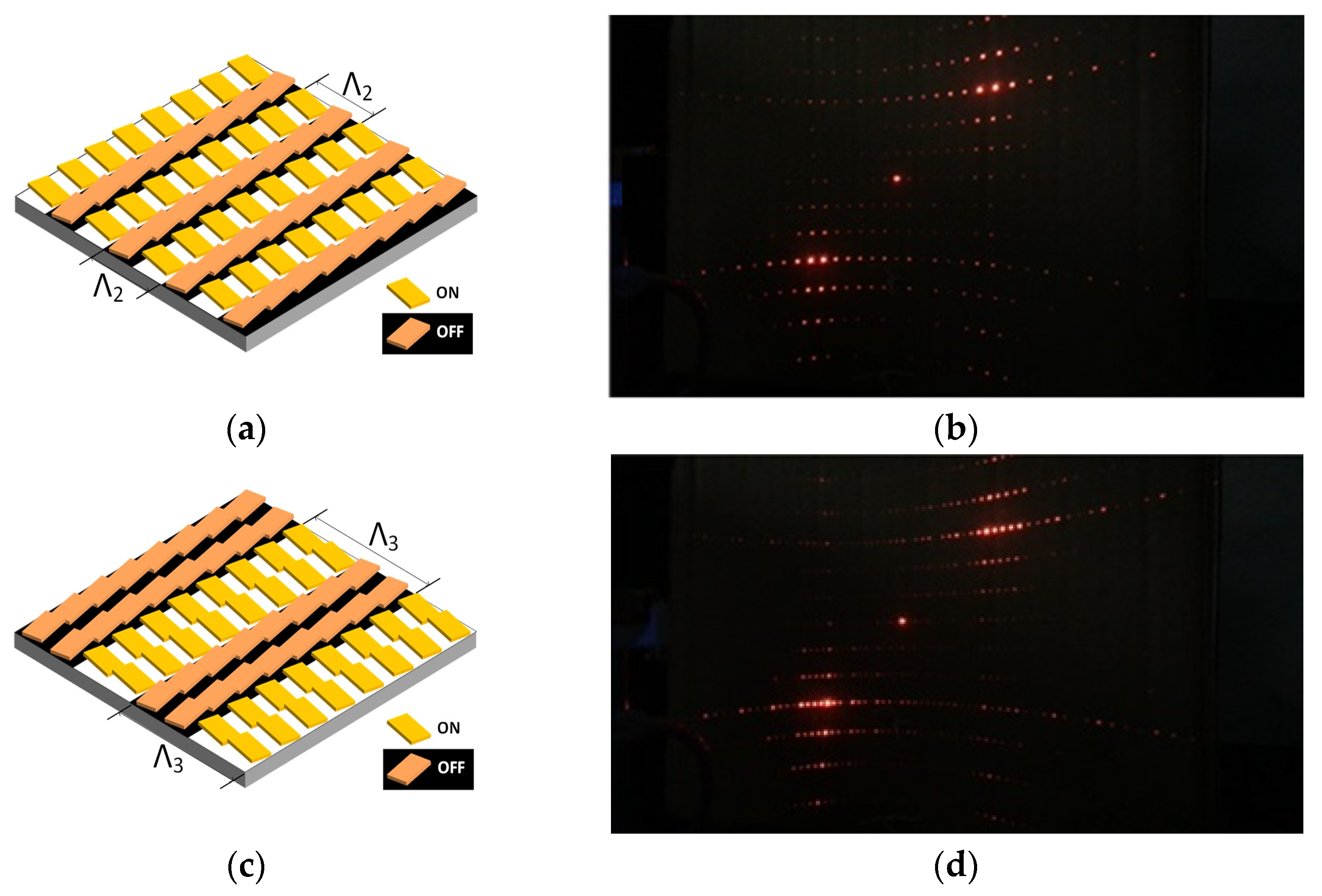
Next, two modulated DMD patterns were investigated.
Figure 3a shows the schematic of a DMD pattern with a period of one line ON-state (white stripe) and one line OFF-state (black stripe). In this configuration, the grating period indicated as Λ
2 was two DMD pixel widths. Because of the two opposite-tilted angles (+12° and −12°) of the micromirrors, two symmetric diffraction spot images were observed on two sides of the center along the −45° line, as shown in
Figure 3b. Because the line grating period Λ
2 was double that of Λ
1 in
Figure 2c, the distance between the two nearest order diffraction spots along the horizontal direction became half of that in
Figure 2c. Because there was no pattern modulation along the other vertical direction, the distance between the two nearest diffractive spots along the vertical direction was the same as that in
Figure 2c. To implement the digital four-phase shifting, a DMD pattern with a period of Λ
3 having four-pixel width, including two ON-state (white stripe) and two OFF-state (black stripe) line pixels, was required. Its schematic and corresponding diffraction spot image are shown in
Figure 3c,d, respectively. Because the grating pitch Λ
3 was twice Λ
2, the distance between two diffraction spots along the horizontal direction became only half of that in
Figure 3b. The phase difference between the two nearest order diffraction lights could be changed by shifting this DMD line pattern to implement the phase shifting in a PSI system. The number of reflecting mirrors and their periods did not affect the performance of the PSI system. The mirror period will change the diffraction angle only.
3. DMD-Based PSI System
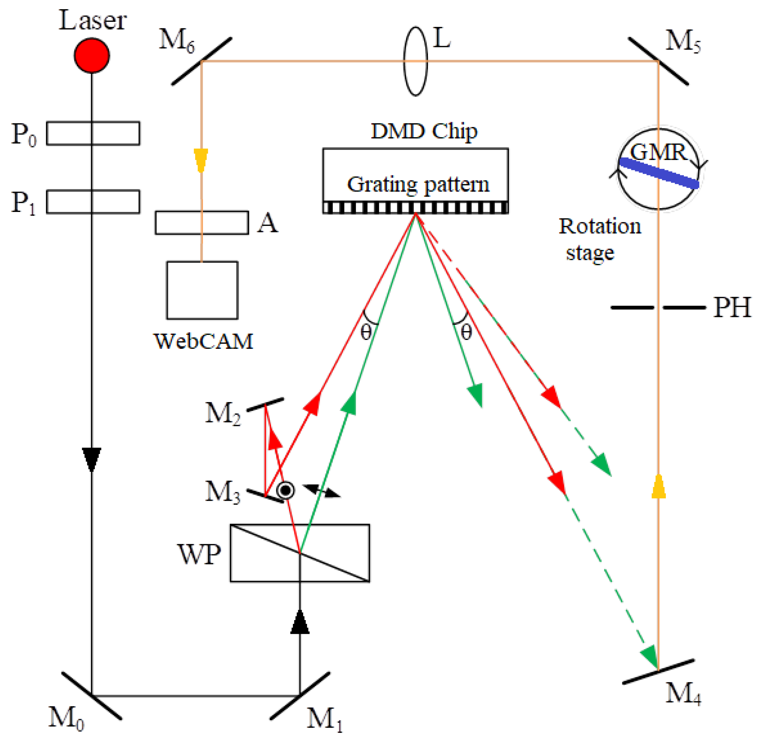
Figure 4 shows the optical setup of the proposed DMD-based PSI system. Here, we used a commercially available DLP LightCrafter display 2000 evaluation module (DLPDLCR 2000EVM, Texas Instruments), comprising a DLP 2000 DMD chip with a resolution of 640 × 480. This is a development kit for micro-projectors and can be controlled via a Beaglebone Black platform. In our system, a He–Ne laser was used as the light source, and two polarizers, P
0 and P
1, were used to vary the incident light intensity. P
1 was rotated 45° to yield output light having both
p- and
s-polarized components. The output light passed through a Wollaston prism (WP) and split into an
s-polarized beam (red line) and a
p-polarized beam (green line) at a separation angle of 15°. The
p-polarized beam was directly incident on the DMD chip, while the
s-polarized beam passed two mirrors (M
2 and M
3) before being incident on the DMD chip. These two mirrors were used to adjust the zeroth-order reflected beam (solid red line) of the
s-polarized light to coincide with the first-order reflected beam (dashed green line) of the
p-polarized incident light. The angle difference
θ between these two incident beams was equal to the difference between the zeroth- and the first-order reflected beams of the
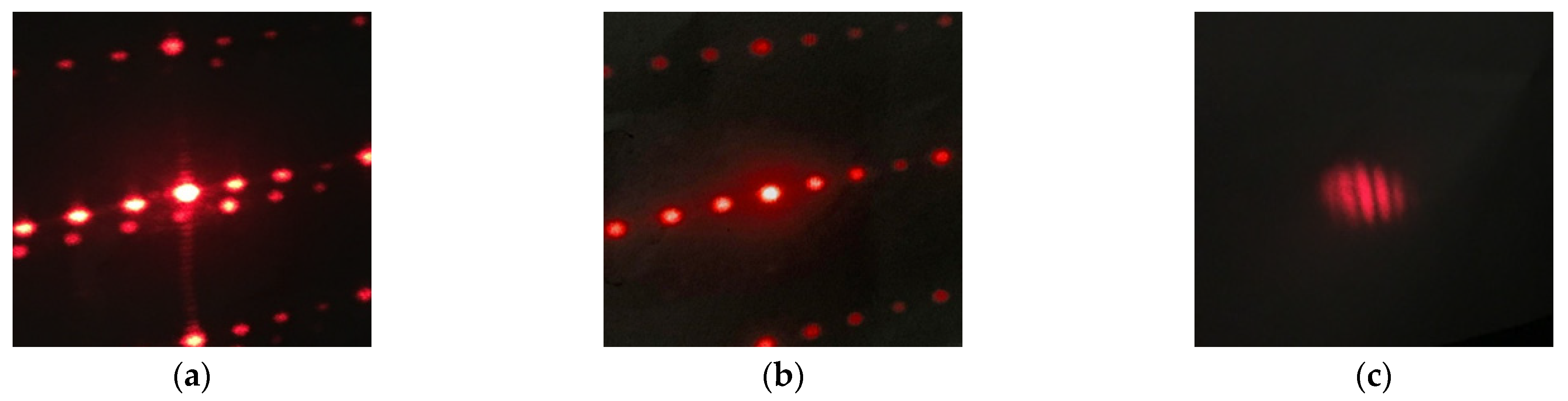
p-polarized light. The phase difference between these two coincided beams could be controlled by the four-line pattern displayed on the DMD chip. This coincided beam was then passed through an aperture (AP) and analyzer (A) and became a measurement beam in the PSI system. After this beam passed through the GMR device, the resulting interferograms were generated and captured by a web camera (WebCAM) (Phillips 900nc). A lens (L) was used to adjust the image size of the interferograms. Diffraction spot patterns of these two reflected beams before and after coinciding are shown in
Figure 5a,b, respectively. The intensity difference between the
s- and
p-polarized beams could be adjusted by rotating the analyzer to have the best contrast of the interferogram. The final enlarged interferogram is shown in
Figure 5c.
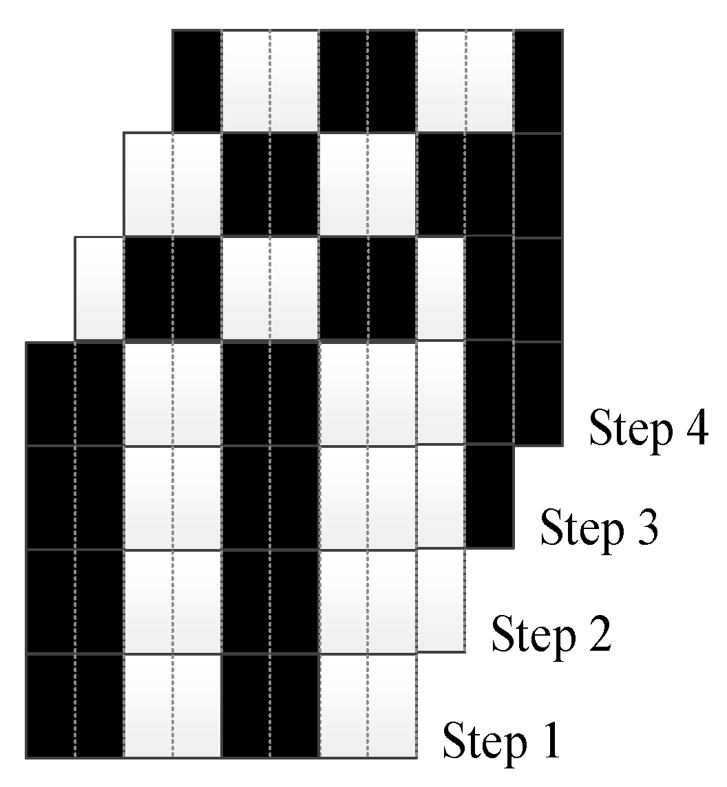
A set of four-step patterns displayed on the DMD-SLM is shown in
Figure 6. The black- and white-stripe colors correspond to two lines of OFF- and ON-states, respectively, on the DMD chip as illustrated in
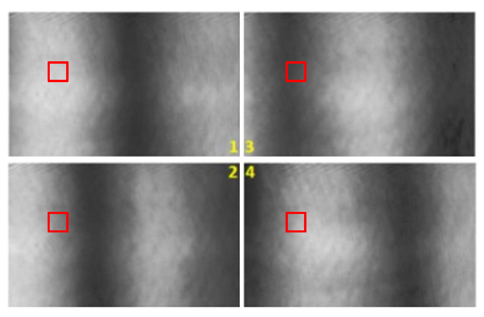
Figure 3c. Each subsequent pattern had one pixel shifting to achieve a phase shift of π/2. Therefore, four digital phase shifts, 0, π/2, π, and 3π/2, could be achieved by sequentially displaying these four patterns on the DMD-SLM. Before performing the GMR sensor measurements, system repeatability was investigated. The GMR device was replaced by a null glass substrate and four interferograms corresponding to the four patterns of
Figure 6 were obtained, as shown in
Figure 7. Because the action of the micromirrors was flipped, not stationary, this could have a time-averaging effect on the laser intensity and reduce the speckle in the interferogram. In each interferogram image, a red square area (10 × 10 pixels) was selected, as indicated in the figure, and their average gray values were used to obtain the average intensity values used in the PSI system. The phase difference between the
s- and
p-polarized lights could be calculated with the 4-step phase-shifting algorithm [
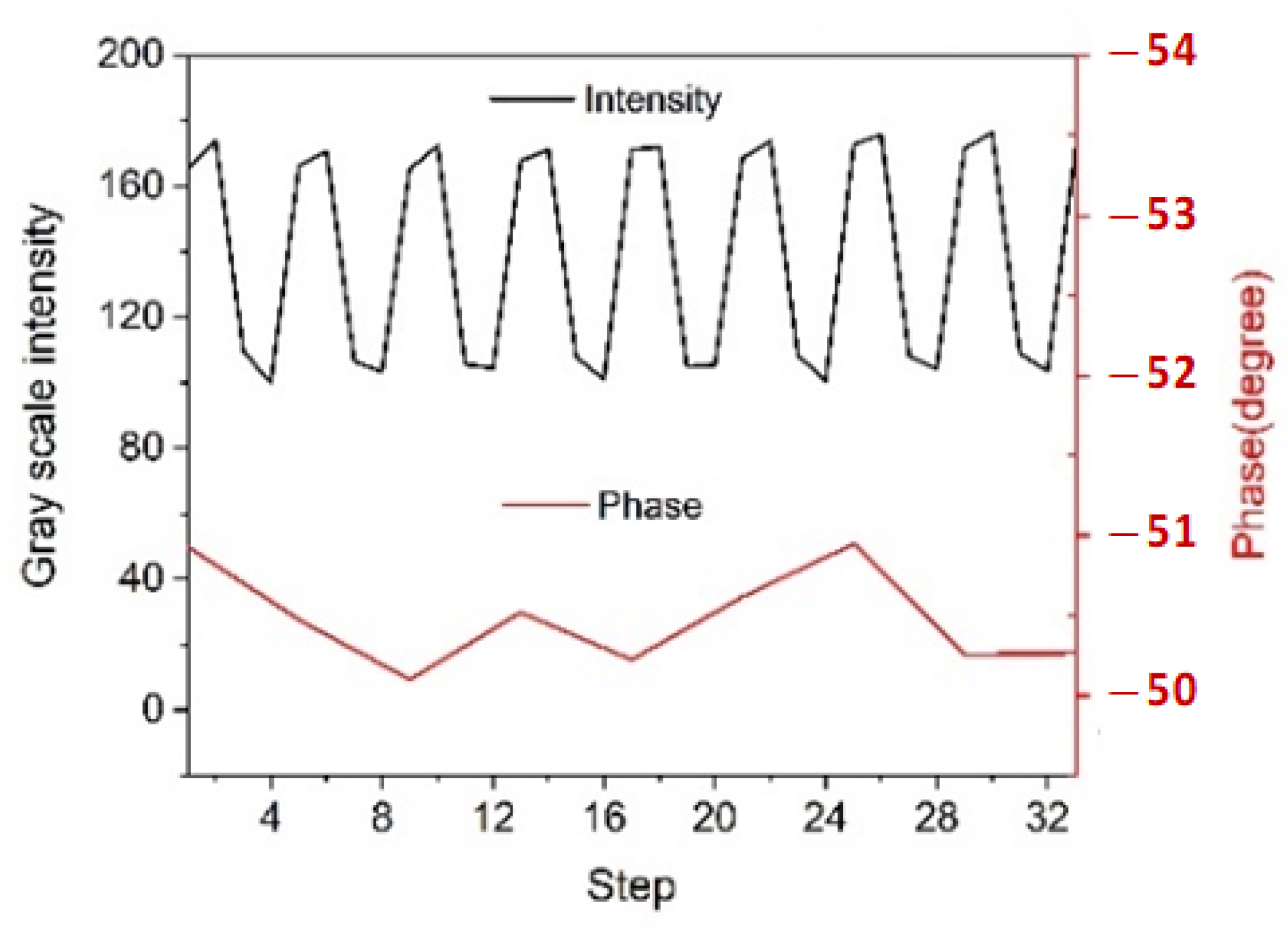
13]. The same condition was repeatedly measured 8 times, and hence, eight phase values were calculated; the results are shown in
Figure 8. The upper curve (black) represents the 32 average intensity gray values of the eight sets, whereas the red curve (red) represents the calculated phase values. The variation of the phase values was within 1° and hence, the system detection limit could be estimated to be 1°. This detection limit may be further improved by enhancing the stiffness of the PSI system.
4. GMR Device Measurement Results
Finally, the setup was used to measure the phase difference between the
s- and
p-polarized light beams passing through the GMR device. Under the resonance condition, the angular transmission phase of the GMR device had a large phase change known as Goos-Hänchen (GH) shift [
14,
15]. The resonance angles of the GMR device for the
s- and
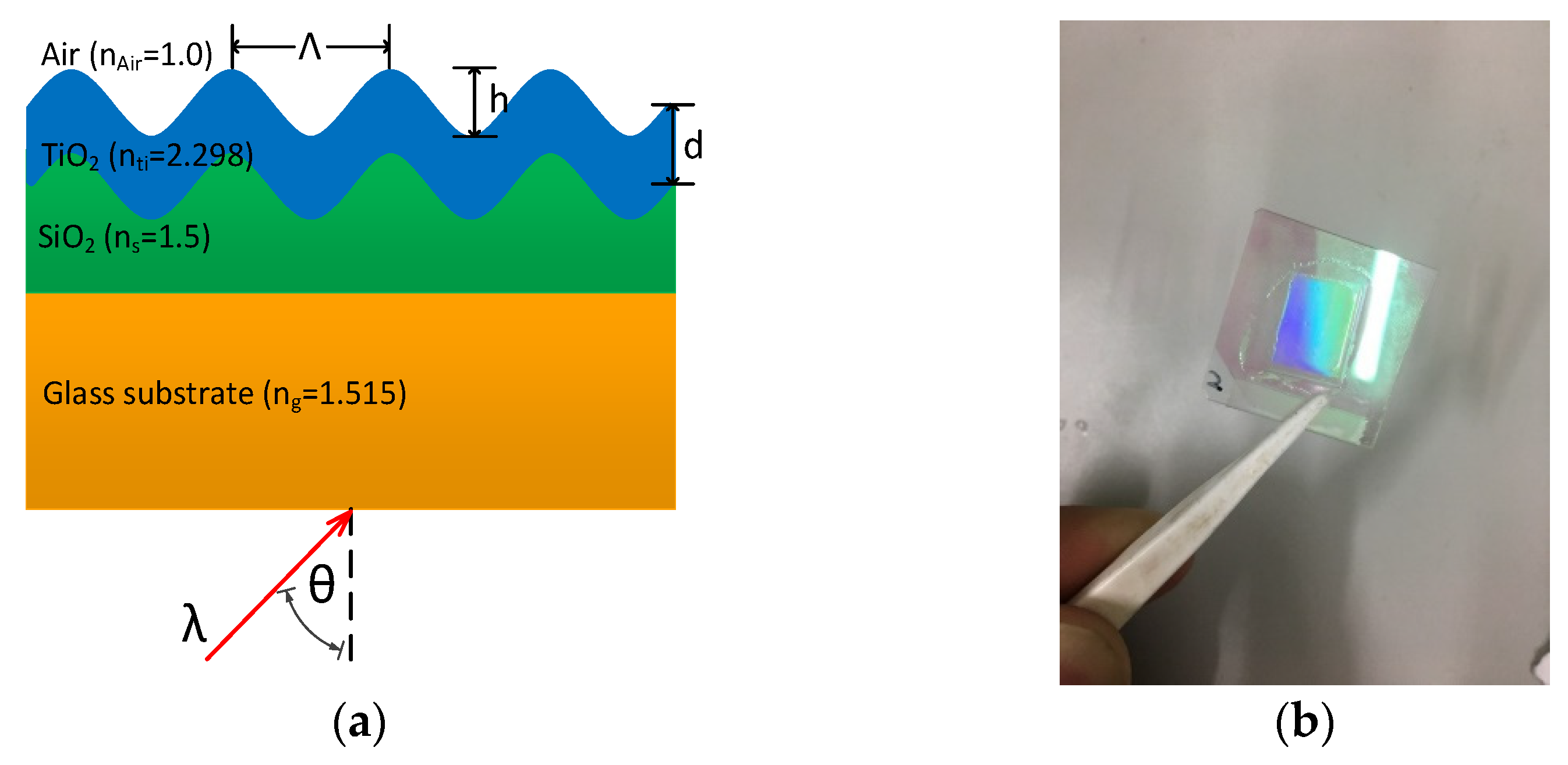
p-polarized light beams were different, and the proposed DMD-based PSI system was able to measure the phase difference between the resonance angle and non-resonance angle. The schematic of the tested GMR device is shown in
Figure 9a; the device is similar to the one in our previous report [
6]. The device was fabricated on a glass substrate and comprised a TiO
2 thin-film layer with a thickness
d of 325 nm, a SiO
2 grating layer with a period Λ of 555 nm, and modulation depth
h of 65 nm. The grating structure was fabricated by using the nanoimprinting sol-gel method. A photograph of the completed GMR sensor is shown in
Figure 9b.
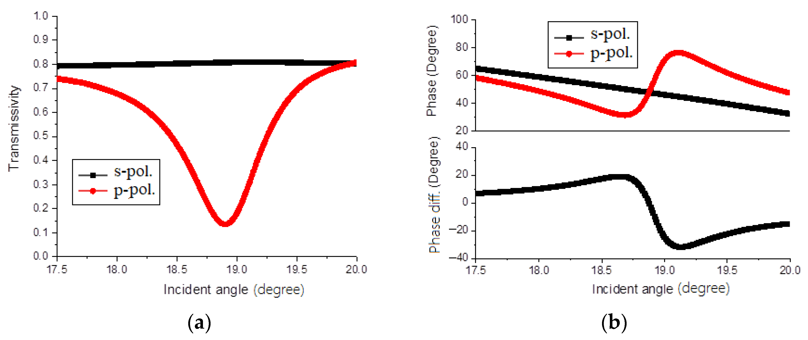
The GMR device was simulated using commercially available finite-difference time-domain (FDTD) software. The GMR device was investigated with the condition that the
p-polarized component of the incident light satisfy the phase-matching condition. The incident light entered at the substrate of the GMR device and the sensor surface was air (
n = 1.0). In simulation, complex refractive
n = 2.298 and extinction coefficient
k = 0.005 of the TiO
2 thin-film layer were used. The extinction coefficient was used to model the loss due to all non-ideal effects. The simulation results for the transmissivity versus the scanning incident angle are shown in
Figure 10a. The resonance
p-polarization and the non-resonance
s-polarization are indicated as the red and black lines, respectively, and the resonance angle of
p-polarization is 18.8°. The transmission phases of the GMR device are shown in
Figure 10b. The resonance transmission phase (
p-polarization, red) had an abrupt change near the resonance angle, while the non-resonance phase (
s-polarization, black) had a smooth change due to the incident angle change. The phase difference between the
p- and the
s-polarization component is also shown in
Figure 10b. This phase difference can be measured by the proposed DMD-based PSI system.
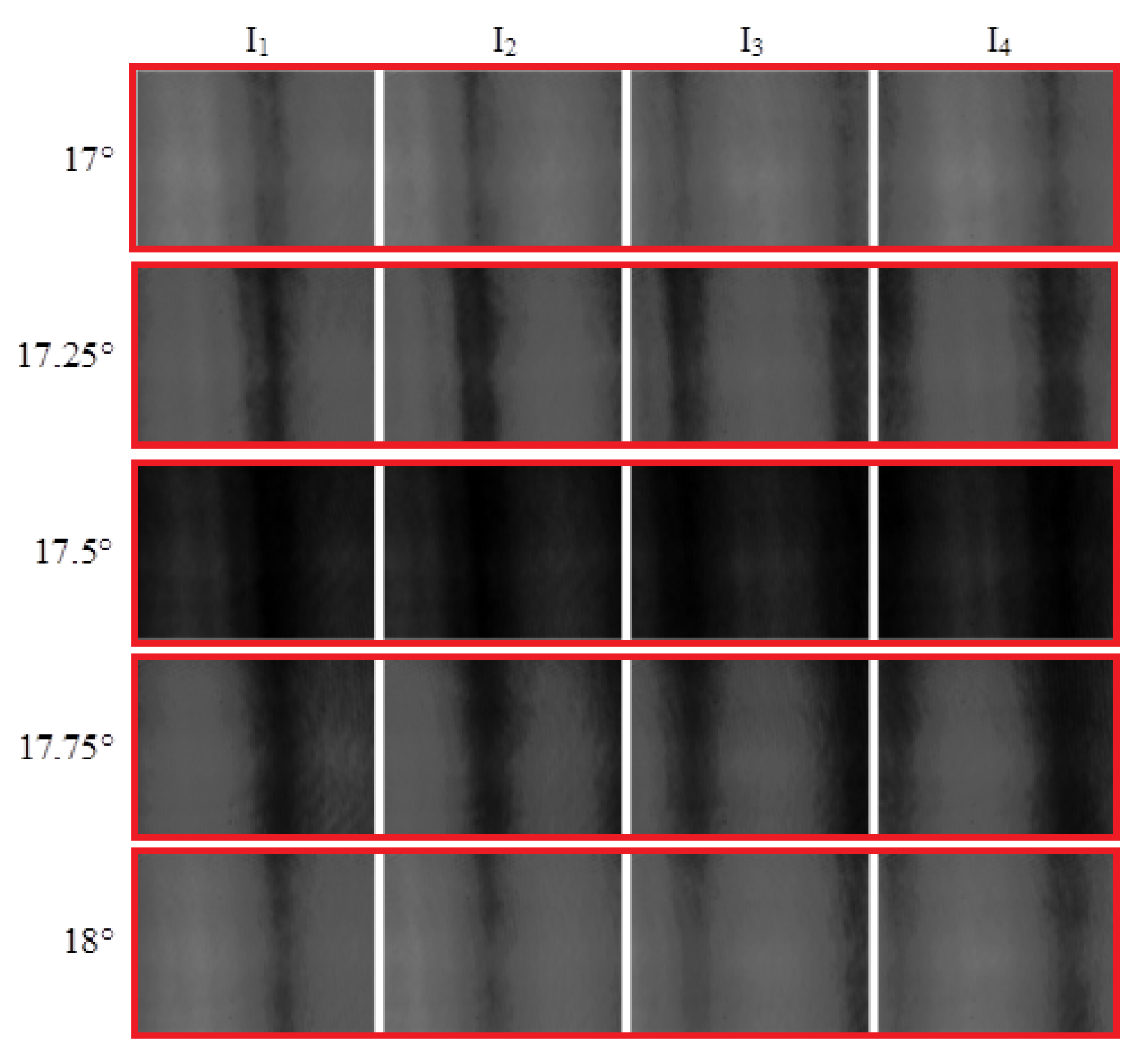
For the measurements, the GMR device was mounted on a rotation stage as indicated in
Figure 4, and the incident angle was varied from 16° to 18.5° with an interval of 0.05° by rotating the stage. Five selected sets of four-step interferograms (I
1~I
4) (in a red-color rectangle line) corresponding to four incident angles, 17°, 17.25°, 17.5°, 17.75°, and 18°, are shown in
Figure 11, and each set of the four-step interferograms was used to calculate phase values by applying the 4-step phase-shifting algorithm to the selected square area, as shown in
Figure 7. The five sets of interferograms were selected to demonstrate the variation of the grayscale values due to the resonance angle. The average intensities of the interferograms decreased from 17° to 17.25° as the incident angle was approaching the resonance angle, reached the minimum at the resonance angle of 17.5°, and then increased from 17.75° to 18° as the incident angle was leaving the resonance angle.
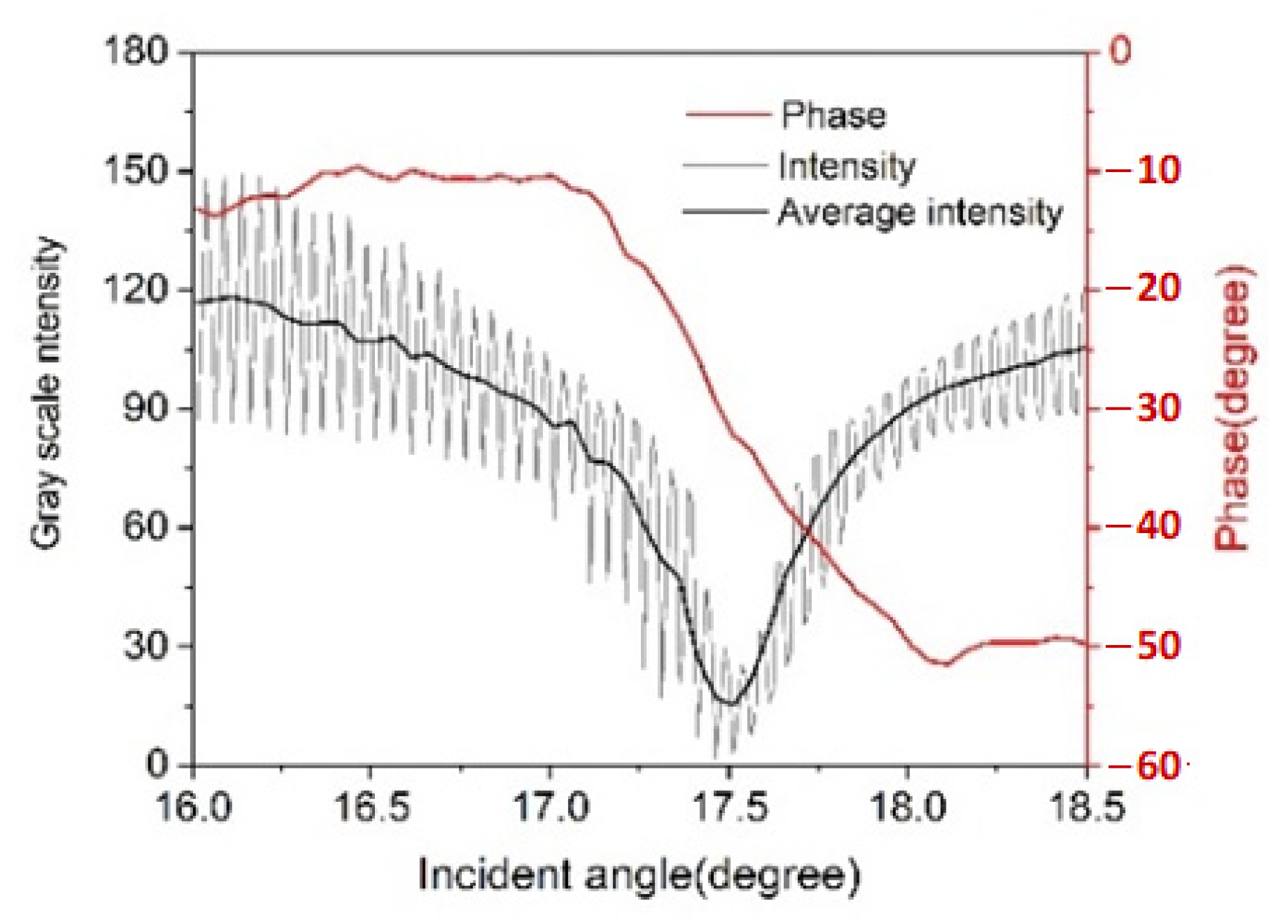
The calculated 50 phase values (red) and 200 (50 × 4) intensities (gray) of the selected areas in all interferograms versus the incident angle are shown in
Figure 12. The obtained phase curve corresponded to the phase difference between
s- and
p-polarization components and agreed with the simulation in
Figure 10b. The black line is the average transmitted intensity and corresponds to the transmissivity in
Figure 10a. The resonance angle can be found as 17.5°, and the phase curve exhibited an abrupt change near the resonance angle. The simulation results have a larger resonance angle and phase dynamic range than the measured values; these discrepancies may be due to the parameters of the fabricated GMR device, which were not the same as those used in the simulation model. In
Table 1, this system is compared with other phase measurement studies of the GMR device.


