Communication

Novel Low-Loss Fiber-Chip Edge Coupler for Coupling Standard Single Mode Fibers to Silicon Photonic Wire Waveguides

Institute of Microelectronics, Chinese Academy of Sciences, Beijing 100029, China
*
Author to whom correspondence should be addressed.
Photonics 2021, 8(3), 79; https://doi.org/10.3390/photonics8030079
Submission received: 10 February 2021 / Revised: 10 March 2021 / Accepted: 11 March 2021 / Published: 16 March 2021
(This article belongs to the Special Issue Optical Technologies for Data Center Networks)

Abstract

:
Fiber-to-chip optical interconnects is a big challenge in silicon photonics application scenarios such as data centers and optical transmission systems. An edge coupler, compared to optical grating, is appealing to in the application of silicon photonics due to the high coupling efficiency between standard optical fibers (SMF-28) and the sub-micron silicon wire waveguides. In this work, we proposed a novel fiber–chip edge coupler approach with a large mode size for silicon photonic wire waveguides. The edge coupler consists of a multiple structure which was fulfilled by multiple silicon nitride layers embedded in SiO2 upper cladding, curved waveguides and two adiabatic spot size converter (SSC) sections. The multiple structure can allow light directly coupling from large mode size fiber-to-chip coupler, and then the curved waveguides and SSCs transmit the evanescent field to a 220 nm-thick silicon wire waveguide based on the silicon-on-insulator (SOI) platform. The edge coupler, designed for a standard SMF-28 fiber with 8.2 μm mode field diameter (MFD) at a wavelength of 1550 nm, exhibits a mode overlap efficiency exceeding 95% at the chip facet and the overall coupling exceeding 90%. The proposed edge coupler is fully compatible with standard microfabrication processes.

1. Introduction

Recently, explosive growth in data analytics applications such as cloud computing, video streaming and online gaming are leading to a convergence between datacenters and high-performance computing (HPC) systems [1,2,3]. To satisfy such demands, large-scale studies have been developed towards intra-datacenter optical interconnects based on the silicon photonics platform via single mode fibers (SMF) in the last one kilometer [4,5]. The silicon photonics attracts intense interests due to its ultra-compact and low-cost characteristics. However, mode size mismatch between SMF-28 and sub-μm silicon wire waveguide lets the light suffer from a rather low mode overlap efficiency over a broad spectrum [6,7].
Two kinds of approaches can be used to solve this problem, namely the edge coupler and surface grating coupler [8,9,10]. Surface grating coupler, that is out of plane coupling, can couple light from a fiber into a silicon wire waveguide at a nearly vertical degree to maintain a high coupler efficiency, and vice versa. The grating coupler is capable of wafer-level testing and enhancing on-chip compactness. However, for a uniform grating coupler based on a standard 220 nm-thick silicon silicon-on-insulator (SOI) platform, there are also some disadvantages such as low coupling efficiency, wavelength and polarization sensitivity, which make them inappropriate for WDM applications [11,12,13]. As for the butt coupling or package with conventional cleaved optical fiber, the edge coupler is more convenient to use, which can achieve higher coupling efficiency, a much more flexible operating wavelength and less dependence on polarization than grating coupler [7,14].
Spot size converter (SSC) can usually be used in an edge coupler to expand the mode at the narrow tip which is nearly as large as the fiber mode. Then, this delocalized mode is transformed to a highly confined mode in silicon wire waveguide through slowly increasing the waveguide width. However, this is hard to achieve a large mode size in an SOI waveguide. A trident SSC is proposed to be hybrid integrated with a light source on a silicon platform [8,12]. This SSC exhibits low polarization dependence and a low coupling loss at 1550 nm wavelength. However, it includes an ultra-narrow tip which increases the fabrication complexity and cost. In order to improve the coupling efficiency with a large mode size fiber, Papes et al. [15] proposed a new fiber–chip edge coupler coupling from a standard SMF-28 fiber with a 10.4 μm mode field diameter (MFD) at 1550 nm to a silicon photonic wire waveguide. This edge coupler is designed by implementing in the SiO2 upper cladding three high-index Si3N4 layers. Through adding a sub-wavelength grating behind the Si3N4 layers horizontally, the overall coupling efficiency is 84%. Nevertheless, the device is too long and the fabrication tolerance of Si3N4 layer thickness is low, which make it troublesomely in practice. In order to reduce the edge coupler length, Sisto et al. [4] presented a sort of edge coupler based on a cross-like arrangement of SiOxNy waveguides inserted in a SiO2 cladding region. The device will exhibit 0.7 dB overall loss with a total length of 450 μm, but this is at the expense of high fabrication complexity such as the uniform SiOxNy material growth which is inconveniently available [10,16,17]. An interesting approach is demonstrated by Dangel et al. using the polymer waveguide with a fundamental mode matching the single mode fiber mode. They obtain less than 3.5 dB coupling loss across the O-band from the SMF to the silicon waveguide, giving the chance to be used in broadband and polarization independent optical packaging [18].
In this work, we present a novel CMOS-compatible edge coupler optimized for light coupling from a standard SMF fiber with 8.2 μm MFD at 1550 nm to a silicon photonic wire waveguide based on a standard 220 nm-thick silicon SOI platform. By optimizing the structures of the edge coupler, it exhibits 95 and 99% mode overlap efficiencies at the chip facet for transverse electric (TE) mode and transverse magnetic (TM) mode at 1550 nm wavelength, respectively. The overall coupling efficiency of a less than 895 μm-edge coupler is exceeding 90% for the TE mode through managing the SSCs. The designed edge coupler exhibits a high mode overlap efficiency with a large mode size, high overall coupling efficiency, high compactness, and CMOS-compatible performances.

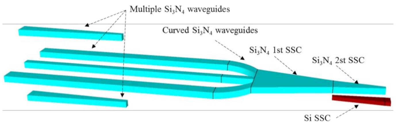
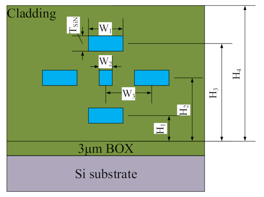
2. Materials and Methods

The overall coupling efficiency can be expressed as two parts: the mode overlap efficiency between fundamental fiber mode and the delocalized mode at the chip facet, and the mode transformation efficiency. When one mode is dominant, the modal overlap efficiency can be given as follows [19]:
η 1 = E 1 E 2 d A 2 E 1 2 d A E 2 2 d A
where E1 and E2 are complex electric field amplitudes of the delocalized mode at the chip facet and fiber mode. The mode transformation efficiency describes how much the light transforms from the chip facet to the silicon photonic wire waveguide. Apart from coupling efficiency, another parameter, coupling loss, is usually used to describe how much energy is lost during light transmission, which is given as follows:
CL = 10 × log 10 η
where CL and η are the coupling loss and coupling efficiency, respectively.
The 3-D full schematic of edge coupler structure, shown in Figure 1, can transform the delocalized mode at the chip facet supported by multiple Si3N4 layers to a highly confined mode of the silicon wire waveguide. The edge coupler is made up of five Si3N4 waveguides in three layers, curved Si3N4 waveguides and two-section Si3N4 SSCs with an engineered propagating mode effective index along the propagation direction. We define these three Si3N4 layers as the upper layer, middle layer and lower layer, according to the vertical position. The Si3N4 SSCs in the upper layer and lower layer are identical with the width reducing from 340 to 180 nm for the decreasing mode effective indexes. In the middle layer, the waveguide in the center is narrower than those on the sides. After the lower layer and upper layer termination points, the modes are separated in three waveguides of middle layer and then transformed to one mode through the curved waveguides. Until now, this edge coupler has transformed a delocalized mode as large as a fiber mode to one single mode in a Si3N4 waveguide. Then, we used two-section Si3N4 SSCs to evanescently couple the light from the Si3N4 waveguide to a silicon wire waveguide. The mode in the silicon wire waveguide can be used in silicon integrated devices, such as the modulator and the photodetector.
The cross-section schematic of the designed edge coupler near the chip facet is shown in Figure 2. The proposed edge coupler is formed by a cross-shaped arrangement of five Si3N4 waveguides surrounded by SiO2 cladding layers. The substrate is SOI with a 3 μm-thick buried oxide(BOX). Through optimizing the spacing and widths of Si3N4 waveguides, we can obtain only one collective TE or TM mode rather than separate modes in each waveguide.

3. Simulation Results

We studied the mode overlap efficiencies for the TE and TM mode, and the overall coupling efficiency for the TE mode only, using MODE solutions software from Lumerical. The simulation of mode overlap between the fiber and edge coupler facet was carried out with the finite difference eigenmode (FDE) solver. The mode transformation along the coupler is simulated by fully vectorial 3D eigenmode expansion (EME) solver.

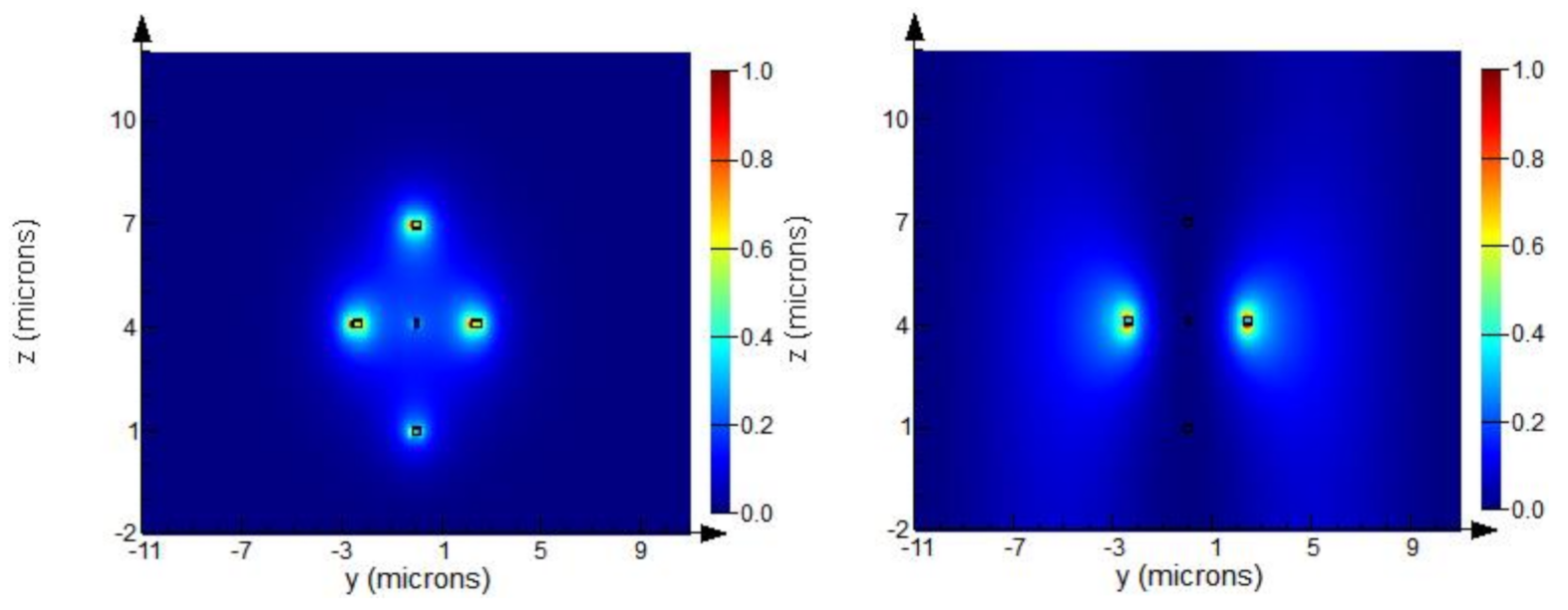
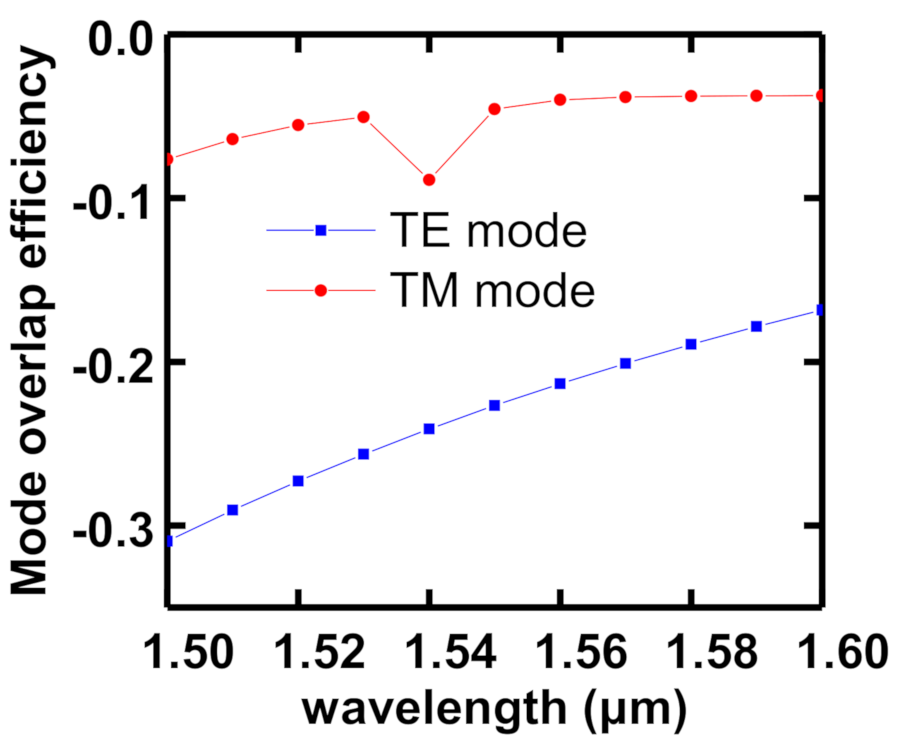
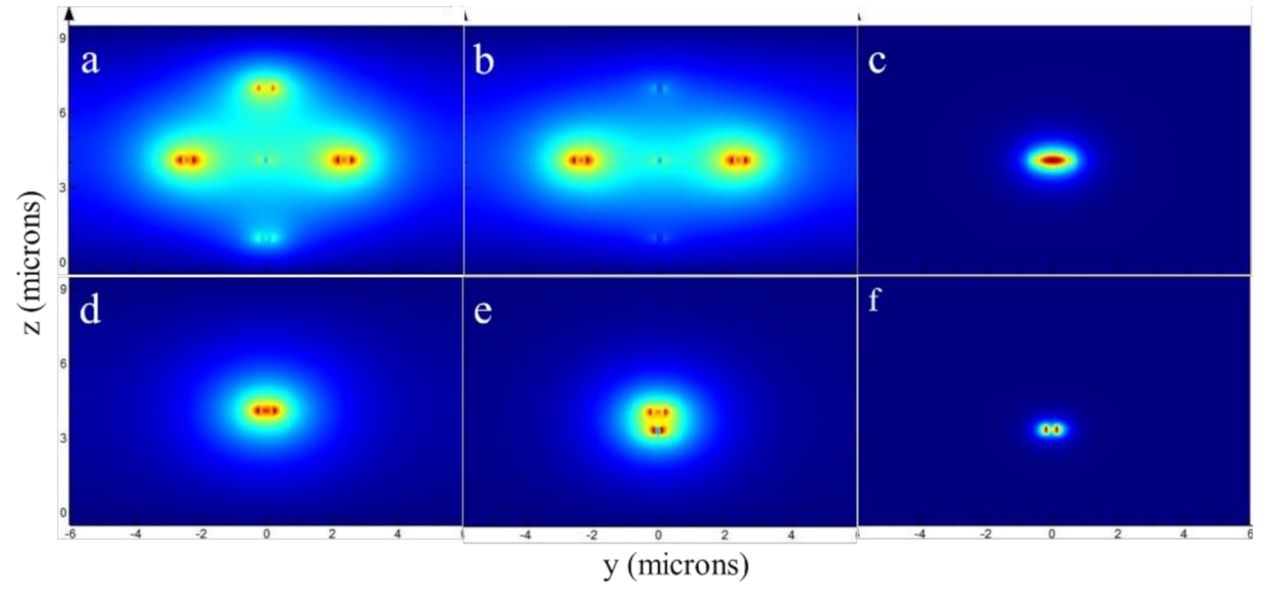
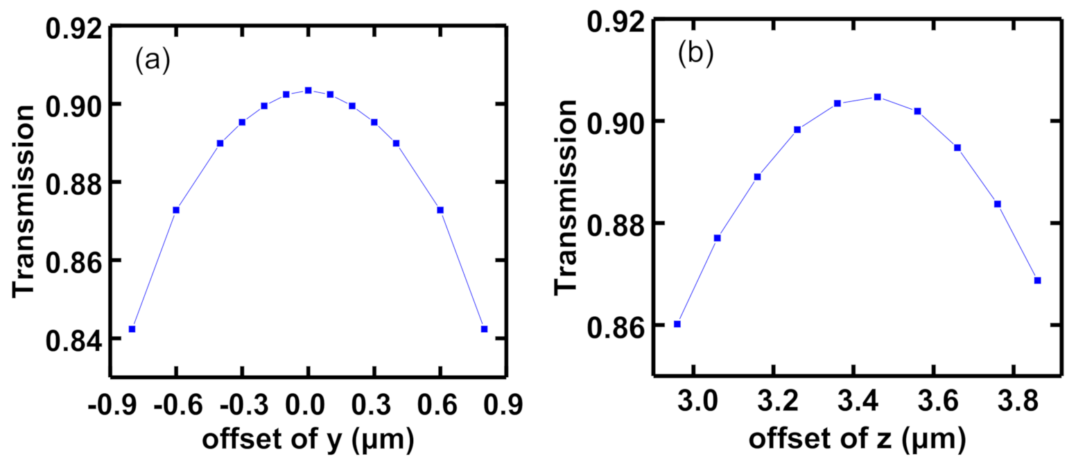
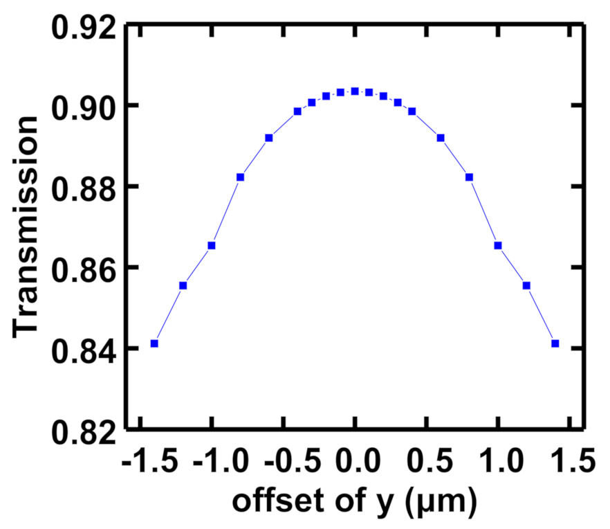
3.1. Mode Overlap Optimization

The cross-shaped arrangement of the edge coupler near the chip facet is shown in Figure 1. The coupler, based on an SOI substrate with 3 μm BOX layer, is constituted of three Si3N4 layers surrounding by SiO2 cladding region. The refractive indexes of Si3N4, Si and SiO2 in material database are 2.016, 3.476 and 1.444 at 1550 nm, respectively.
The high refractive index contrast between silicon and silicon dioxide makes it impossible to expand the mode as large as in optical fiber mode. Thus, a low refractive index material, Si3N4, was considered. We decide to use five Si3N4 waveguides cross-shaped distributed in three layers. By controlling the cladding layer thickness, each Si3N4 waveguide thickness and width, the Si3N4 waveguides can pull the mode spatial distribution towards the upper cladding layer, extremely reduced the leakage to the substrate.
The edge coupler is designed for high coupling with standard SMF-28 fiber with 8.2 μm MFD. This high MFD fiber shows excellent alignment tolerance compared to the lensed fiber, and it is cheap and additionally easy to prepare. The edge coupler comprises a 3 μm-thick BOX layer, a 9.5 μm-thick SiO2 upper cladding layer, a 220 nm-thick silicon wire waveguide and five 200 nm-thick Si3N4 waveguides distributed in three layers. The SiO2 thickness between upper layer and middle layer, middle layer and lower layer is 2.88 and 3.12 μm, respectively. More detailed information about optimized waveguides is listed in Table 1. The simulated fundamental TE and TM polarized mode are shown in Figure 3. It is a collective mode of five waveguides rather than several separate modes in each waveguide. It is obvious that the modes are pulled towards the upper cladding layer. The fundamental TE mode effective indexes in fiber and the edge coupler facet are 1.436 and 1.447, respectively. The mode overlap efficiency between the edge coupler facet and fiber is calculated to be 95% for the TE mode and 99% for TM mode.
Figure 4 presents the simulation results for the wavelength dependence of the mode overlap efficiency of TE and TM modes. The TE mode overlap coupling loss between the edge coupler facet and the optical fiber is as low as 0.17 dB and remains below 0.31 dB over 100 nm centered at 1550 nm, while the TM mode displays a 0.04–0.08 dB coupling loss. The important parameter polarization dependent loss (PDL) is defined as the difference of TE and TM mode coupling efficiency [12]. It can be negligible over the whole wavelength sweep range.

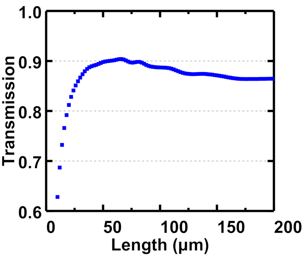
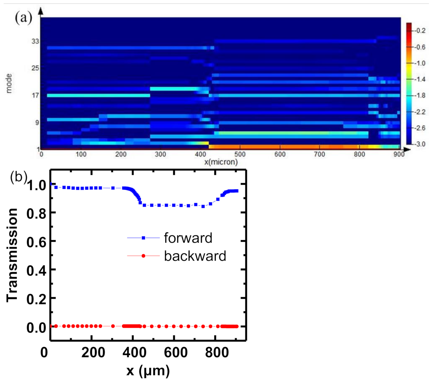
3.2. Mode Transformer Design

The mode transformer is designed using a 3D EME solver, from Lumerical, which is appealing to calculate large structures because it takes less time. The EME method is convenient and fast to sweep the length of SSC by calculating the modes and overlaps between two adjacent cells in advance.
The 3D-EME results are given in Figure 5. Panels (a–f) show the transverse mode distributions at different points along the edge coupler, namely at the edge coupler facet, at the upper (or lower) Si3N4 waveguide termination point, at curved waveguide termination point, at 36 μm before the Si3N4 first SSC termination point, at the Si3N4 first SSC termination point, and in the highly confined mode of the silicon wire waveguide. The simulated mode overall coupling efficiency is above 90% for the totally 895 μm-edge coupler, corresponding to an overall coupling loss of 0.44 dB.
Figure 6 presents the 3D-EME results about the edge coupler transmission to the fundamental mode as a function of second-section SSC length. Before the calculation, we performed the convergence testing. It was shown that the Si3N4 second SSC length of 66 μm can achieve better than 90% overall coupling efficiency. Beyond 66 μm, the total transmission starts to decrease due to light leakage losses. In EME, the large enough transverse simulation size and refined mesh are set to obtain an accurate and high simulation result.
The proposed edge coupler shows great relaxation in lithography alignment tolerances. Figure 7 presents the simulated alignment tolerances between the Si3N4 first SSC and silicon SSC in the direction of the waveguide width (y axis) and material growth (z axis). The edge coupler exhibits at least 84% transmission efficiency aligning silicon SSC in the y axis within 1.8 μm accuracy, while at least 86% transmission efficiency aligning silicon SSC in the z axis within 0.9 μm accuracy.
The alignment tolerance of the upper Si3N4 waveguide in the y axis is also performed and the simulation result is shown in Figure 8. The edge coupler exhibits at least 84% transmission efficiency aligning with the upper Si3N4 waveguide in the y axis within 2.8 μm accuracy. Compared with Figure 7a, the alignment of the upper Si3N4 waveguide is a more relaxed aspect than silicon SSC to define the coupling efficiency. In addition, the same alignment tolerance is for the lower Si3N4 waveguide, as in the symmetric multiple Si3N4 waveguides.
We examined the magnitude of the forward propagating mode coefficients along the length of edge coupler and Figure 9a shows the dependence in the logarithmic coordinate. In Figure 9a, x axis indicates the position in the designed edge coupler from the chip facet to the end of silicon wire waveguide, and the y axis indicates the number of modes totally calculated in each cross section. The color bar is oversaturated on purpose to highlight the magnitudes of the higher order mode coefficients. The results show that the delocalized mode at the chip facet can adiabatically transform to a silicon wire waveguide in fundamental mode whose magnitude is close to 1 at all positions. In Figure 9a, when light travels into the Si3N4 first SSC, the high order mode appears. Meanwhile, in Figure 9b, it records the magnitude of the forward and backward propagating fundamental mode coefficients along the length of edge coupler. In contrast to Figure 9a, it is at the same position that the magnitude of forward propagating fundamental mode exhibits a slight decrease due to high order modes generation. At the end of the Si3N4 first SSC, the high order modes almost transform into fundamental mode, thus the magnitude of forward propagating fundamental mode increases. Additionally, further design improvements can be studied by optimizing the SSC structure in this region to eliminate high order modes.

4. Conclusions

We proposed a novel edge coupler design based on a cross-shaped arrangement of Si3N4 waveguides surrounded by SiO2 cladding layer on a standard 220 nm-thick silicon SOI platform. This edge coupler can couple the light from a standard SMF-28 fiber with 8.2 μm MFD at 1550 nm to silicon wire waveguide with the overall coupling efficiency exceeding 90% (0.44 dB). The advantages of the proposed structure are extremely high mode overlap efficiency to standard 8.2 μm MFD SMFs with 0.04–0.08 dB coupling loss over 100 nm wavelength range centered at 1550 nm; the overall coupling efficiency exceeding 90% in less than 895 μm; the edge coupler shows relaxed alignment tolerances for CMOS fabrication; the edge coupler is fully compatible with standard microfabrication processes. Our results are promising in fiber–chip interconnects applied in data centers and optical transmission systems.

Author Contributions

Conceptualization, S.S. and F.L.; simulation and model development, S.S.; formal analysis, Y.S.; data curation, Y.C.; validation and discussion of the results, S.S. and L.C.; writing—original draft preparation, S.S.; writing—review and editing, S.S. and F.L.; supervision, L.C. All authors have read and agreed to the published version of the manuscript.

Funding

This research received no external funding.

Institutional Review Board Statement

Not applicable.

Informed Consent Statement

Not applicable.

Data Availability Statement

Not applicable.

Conflicts of Interest

The authors declare no conflict of interest.

References

  1. Glick, M.; Abrams, N.C.; Cheng, Q.; Teh, M.Y.; Hung, Y.H.; Jimenez, O.; Liu, S.; Okawachi, Y.; Meng, X.; Johansson, L.; et al. PINE: Photonic Integrated Networked Energy efficient datacenters (ENLITENED Program). J. Opt. Commun. Netw. 2020, 12, 443–456. [Google Scholar] [CrossRef]
  2. Urata, R.; Liu, H.; Verslegers, L.; Johnson, C. Silicon photonics technologies: Gaps analysis for datacenter interconnects. In Topics in Applied Physics; Springer: Berlin/Heidelberg, Germany, 2016; Volume 122, pp. 473–488. ISBN 9783642105036. [Google Scholar]
  3. El-Fiky, E.; Samani, A.; Patel, D.; Jacques, M.; Sowailem, M.; Plant, D.V. 400 Gb/s O-band silicon photonic transmitter for intra-datacenter optical interconnects. Opt. Express 2019, 27, 10258. [Google Scholar] [CrossRef] [PubMed]
  4. Sisto, M.M.; Fisette, B.; Paultre, J.-E.; Paquet, A.; Desroches, Y. Novel spot size converter for coupling standard single mode fibers to SOI waveguides. In Proceedings of the Conference on Silicon Photonics XI, San Francisco, CA, USA, 14 March 2016; Volume 9752. [Google Scholar]
  5. Songtao, L.I.U.; Xinru, W.U.; Jung, D.; Norman, J.C.; Kennedy, M.; Tsang, H.K.; Gossard, A.C.; Bowers, J.E. High-channel-count 20 GHz passively mode locked quantum dot laser directly grown on Si with 4.1 Tbit/s transmission capacity. OPTICA 2019, 6. [Google Scholar] [CrossRef] [Green Version]
  6. Picard, M.-J.; Latrasse, C.; Larouche, C.; Painchaud, Y.; Poulin, M.; Pelletier, F.; Guy, M. CMOS-compatible spot-size converter for optical fiber to sub-μm silicon waveguide coupling with low-loss low-wavelength dependence and high tolerance to misalignment. In Proceedings of the Conference on Silicon Photonics XI, San Francisco, CA, USA, 14 March 2016; Volume 9752. [Google Scholar]
  7. Mu, X.; Wu, S.; Cheng, L.; Fu, H.Y. Edge couplers in silicon photonic integrated circuits: A review. Appl. Sci. 2020, 10, 1538. [Google Scholar] [CrossRef] [Green Version]
  8. Hatori, N.; Shimizu, T.; Okano, M.; Ishizaka, M.; Yamamoto, T.; Urino, Y.; Mori, M.; Nakamura, T.; Arakawa, Y. A hybrid integrated light source on a silicon platform using a trident spot-size converter. J. Light. Technol. 2014, 32, 1329–1336. [Google Scholar] [CrossRef]
  9. Almeida, V.R.; Panepucci, R.R.; Lipson, M. Nanotaper for compact mode conversion. Opt. Lett. 2003, 28, 1302–1304. [Google Scholar] [CrossRef]
  10. Voigt, K.; Brulis, V.; Petermann, K.; Zimmermann, L. Study of backend waveguide arrays for adiabatic coupling to Si waveguides. In Proceedings of the 2017 IEEE 14th International Conference on Group IV Photonics (GFP), Grand Hyatt Berlin, Germany, 23–25 August 2017; pp. 143–144. [Google Scholar] [CrossRef]
  11. Cheben, P.; Bock, P.J.; Schmid, J.H.; Lapointe, J.; Janz, S.; Xu, D.-X.; Densmore, A.; Delâge, A.; Lamontagne, B.; Hall, T.J. Refractive index engineering with subwavelength gratings for efficient microphotonic couplers and planar waveguide multiplexers. Opt. Lett. 2010, 35, 2526–2528. [Google Scholar] [CrossRef] [PubMed] [Green Version]
  12. Marchetti, R.; Lacava, C.; Carroll, L.; Gradkowski, K.; Minzioni, P. Coupling strategies for silicon photonics integrated chips. Photonics Res. 2019, 7, 201–239. [Google Scholar] [CrossRef]
  13. Zhao, X.; Li, D.; Zeng, C.; Gao, G.; Huang, Z.; Huang, Q.; Wang, Y.; Xia, J. Compact grating coupler for 700-nm silicon nitride strip waveguides. J. Light. Technol. 2016, 34, 1322–1327. [Google Scholar] [CrossRef]
  14. Ong, J.R.; Ang, T.Y.L.; Alagappan, G.; Son, C.H.; Lim, S.T.; Png, C.E. Silicon nitride double-Tip fiber-To-waveguide edge couplers at visible wavelengths. In Proceedings of the Conference on Lasers and Electro-Optics Pacific Rim (CLEO-PR), Singapore, 31 July–4 August 2017. [Google Scholar]
  15. Papes, M.; Cheben, P.; Benedikovic, D.; Schmid, J.H.; Pond, J.; Halir, R.; Ortega-Moñux, A.; Wangüemert-Pérez, G.; Ye, W.N.; Xu, D.-X.; et al. Fiber-chip edge coupler with large mode size for silicon photonic wire waveguides. Opt. Express 2016, 24, 5026–5038. [Google Scholar] [CrossRef]
  16. Huang, T.; Jin, C.; Yu, J.; Yang, Y.; Zhuge, L.; Wu, X.; Sha, Z. One-Step Synthesis of Silicon Oxynitride Films Using a Steady-State and High-Flux Helicon-Wave Excited Nitrogen Plasma. Plasma Chem. Plasma Process. 2017, 37, 1237–1247. [Google Scholar] [CrossRef]
  17. Aubry, E.; Weber, S.; Billard, A.; Martin, N. Silicon oxynitride thin films synthesised by the reactive gas pulsing process using rectangular pulses. Appl. Surf. Sci. 2011, 257, 10065–10071. [Google Scholar] [CrossRef]
  18. Dangel, R.; La Porta, A.; Jubin, D.; Horst, F.; Meier, N.; Seifried, M.; Offrein, B.J. Polymer waveguides enabling scalable low-loss adiabatic optical coupling for silicon photonics. IEEE J. Sel. Top. Quantum Electron. 2018, 24, 1–11. [Google Scholar] [CrossRef]
  19. Snyder, A.W.; Love, J.D. Optical Waveguide Theory; Springer Science & Business Media: Berlin/Heidelberg, Germany, 1986. [Google Scholar]
Figure 1. Schematic of the designed edge coupler.
Photonics 08 00079 g001
Figure 2. Cross-section schematic of the designed edge coupler near the chip facet.
Photonics 08 00079 g002
Figure 3. The fundamental TE and TM mode at the chip facet for the designed edge coupler.
Photonics 08 00079 g003
Figure 4. Wavelength dependence of mode overlap efficiency between the edge coupler facet and fiber.
Photonics 08 00079 g004
Figure 5. Simulated modal field evolution along the coupler: (a) near the edge coupler facet; (b) upper (or lower) Si3N4 waveguide termination point; (c) curved waveguide termination point; (d) 36 μm before Si3N4 first SSC termination point; (e) Si3N4 first SSC termination point; (f) highly confined mode in the silicon wire waveguide. The simulated mode is quasi-TE mode in 1550 nm.
Photonics 08 00079 g005
Figure 6. The edge coupler transmission to the fundamental mode as a function of Si3N4 second SSC length.
Photonics 08 00079 g006
Figure 7. Alignment tolerances of silicon SSC in the y axis (the direction of the waveguide width) (a) and the z axis (the direction of material growth) (b).
Photonics 08 00079 g007
Figure 8. The alignment tolerance of the upper Si3N4 waveguide in the y axis (the direction of waveguide width).
Photonics 08 00079 g008
Figure 9. (a) The magnitude of the forward propagating mode coefficients along the length of the edge coupler; (b) the magnitude chart of the forward and backward propagating fundamental mode coefficients along the length of edge coupler. In the simulation, 40 modes are calculated.
Photonics 08 00079 g009
Table 1. Optimized parameters of the designed edge coupler.
DimensionSize (μm)
TSiN0.2
W10.34
W20.14
W32.4
H11
H24.12
H37
H49.5
Publisher’s Note: MDPI stays neutral with regard to jurisdictional claims in published maps and institutional affiliations.

