Article

Photothermal, Photoelectric, and Photothermoelectric Effects in Bi-Sb Thin Films in the Terahertz Frequency Range at Room Temperature

by
Mikhail K. Khodzitsky
1,2,*,
Petr S. Demchenko
1,2,
Dmitry V. Zykov
1,2,
Anton D. Zaitsev
1,2,
Elena S. Makarova
2,
Anastasiia S. Tukmakova
2,
Ivan L. Tkhorzhevskiy
2,
Aleksei V. Asach
2,
Anna V. Novotelnova
2 and
Natallya S. Kablukova
2,3
1
Terahertz Biomedicine Laboratory, ITMO University, 197101 Saint-Petersburg, Russia
2
Faculty of Energy and Ecotechnology, ITMO University, 197101 Saint-Petersburg, Russia
3
The Department of Physics, Saint Petersburg State University of Industrial Technologies and Design, 191186 Saint-Petersburg, Russia
*
Author to whom correspondence should be addressed.
Photonics 2021, 8(3), 76; https://doi.org/10.3390/photonics8030076
Submission received: 18 February 2021 / Revised: 10 March 2021 / Accepted: 11 March 2021 / Published: 12 March 2021
(This article belongs to the Special Issue Frontiers in Terahertz Technology and Applications)

Abstract

:
The terahertz frequency range is promising for solving various practically important problems. However, for the terahertz technology development, there is still a problem with the lack of affordable and effective terahertz devices. One of the main tasks is to search for new materials with high sensitivity to terahertz radiation at room temperature. Bi1−xSbx thin films with various Sb concentrations seem to be suitable for such conditions. In this paper, the terahertz radiation influence onto the properties of thermoelectric Bi1−xSbx 200 nm films was investigated for the first time. The films were obtained by means of thermal evaporation in vacuum. They were affected by terahertz radiation at the frequency of 0.14 terahertz (THz) in the presence of thermal gradient, electric field or without these influences. The temporal dependencies of photoconductivity, temperature difference and voltage drop were measured. The obtained data demonstrate the possibility for practical use of Bi1−xSbx thin films for THz radiation detection. The results of our work promote the usage of these thermoelectric materials, as well as THz radiation detectors based on them, in various areas of modern THz photonics.

1. Introduction

The terahertz (THz) or far infrared spectral range is of interest for a number of industrial and research applications, including spectroscopy [1], visualization [2,3], biomedicine [4,5,6], security systems [7], non-destructive material control [8], and even for next-generation wireless communications [9]. Common to all these applications is the problem of finding a high-sensitivity, high-speed, compact THz detector operating at room temperature. Although many materials can actively absorb THz radiation, traditional photoelectric detection methods, when charge carrier is photogenerated and detected electrically, are not applicable at THz frequencies because THz photons have much less energy than optical photons and do not produce excess charge carriers. Therefore, most of the existing THz detectors are based on an electrical measurement of thermal excitation resulting from the absorption of a THz wave, or as a result of a change in resistance, pyroelectric polarization, or acoustic pressure [10]. Devices with superconducting contacts can exhibit high sensitivity to THz-induced heat, but they require cryogenic cooling, which severely limits the field of applications. Despite many recent advances in THz sensor technology, the fastest detectors have low sensitivity, and the most sensitive detectors are usually slow [11]. At the current technological stage, the most commercialized THz detectors are based on traditional semiconductors, such as Si, Ge, and III-nitrides. However, due to physical limitations, they encounter serious problems with scaling down and with integration with Si-platforms, especially in the growing demand for broadband terahertz device operating at room temperature. Thermoelectric materials based on solid solutions of bismuth and antimony have significant potential to solve this problem. Due to the small width of the bandgap, they belong to the class of semimetals with good thermoelectric characteristics [12]. The absorption of THz radiation by semimetals leads to the appearance of additional pairs of charge carriers due to the generation of energy sufficient to transfer an electron to the conduction band, which is similar to the appearance of hot electrons (holes) during the thermoelectric effect [13]. The signal arising due to the photo-thermoelectric effect [14,15] may be enhanced. For this purpose, it is necessary to use a material with a maximum thermoelectric figure of merit for a given ambient temperature. At the same time, the figure of merit of thermoelectrics can be changed under the influence of THz radiation. Seebeck coefficient in A I I I B V bulk crystals is changed under the influence of radiation from the incandescent lamp of different power, which may lead to either strengthen or weaken the thermoelectric effect. In this paper, we aim to study the effect of THz radiation onto the properties of thin-film Bi1−xSbx thermoelectric materials (thermoelectric effect), as well as to search for conditions under which the greatest response in a thermoelectric material is possible as a result of the absorption of THz radiation.

2. Materials and Methods

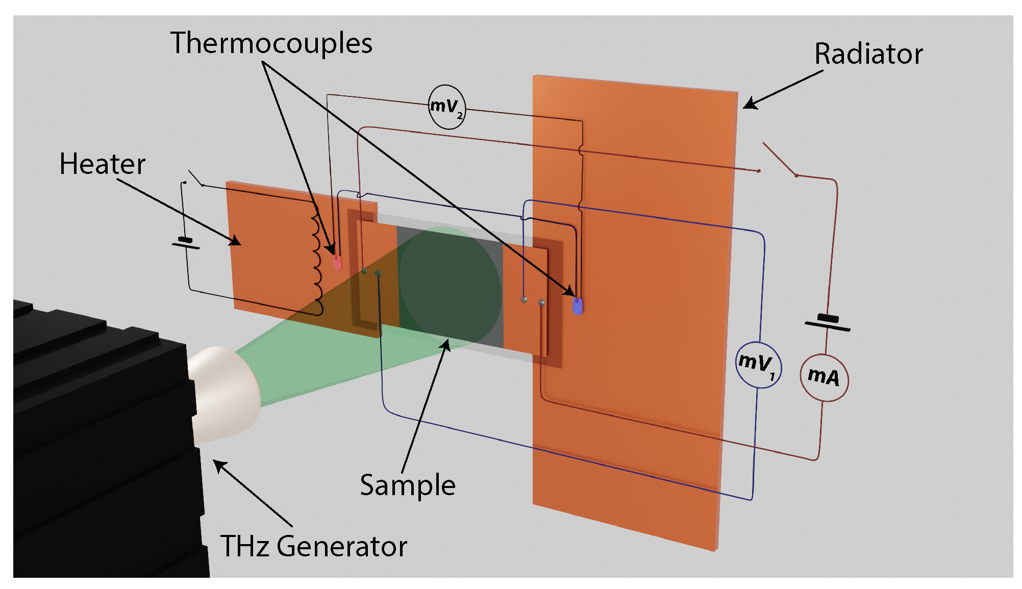
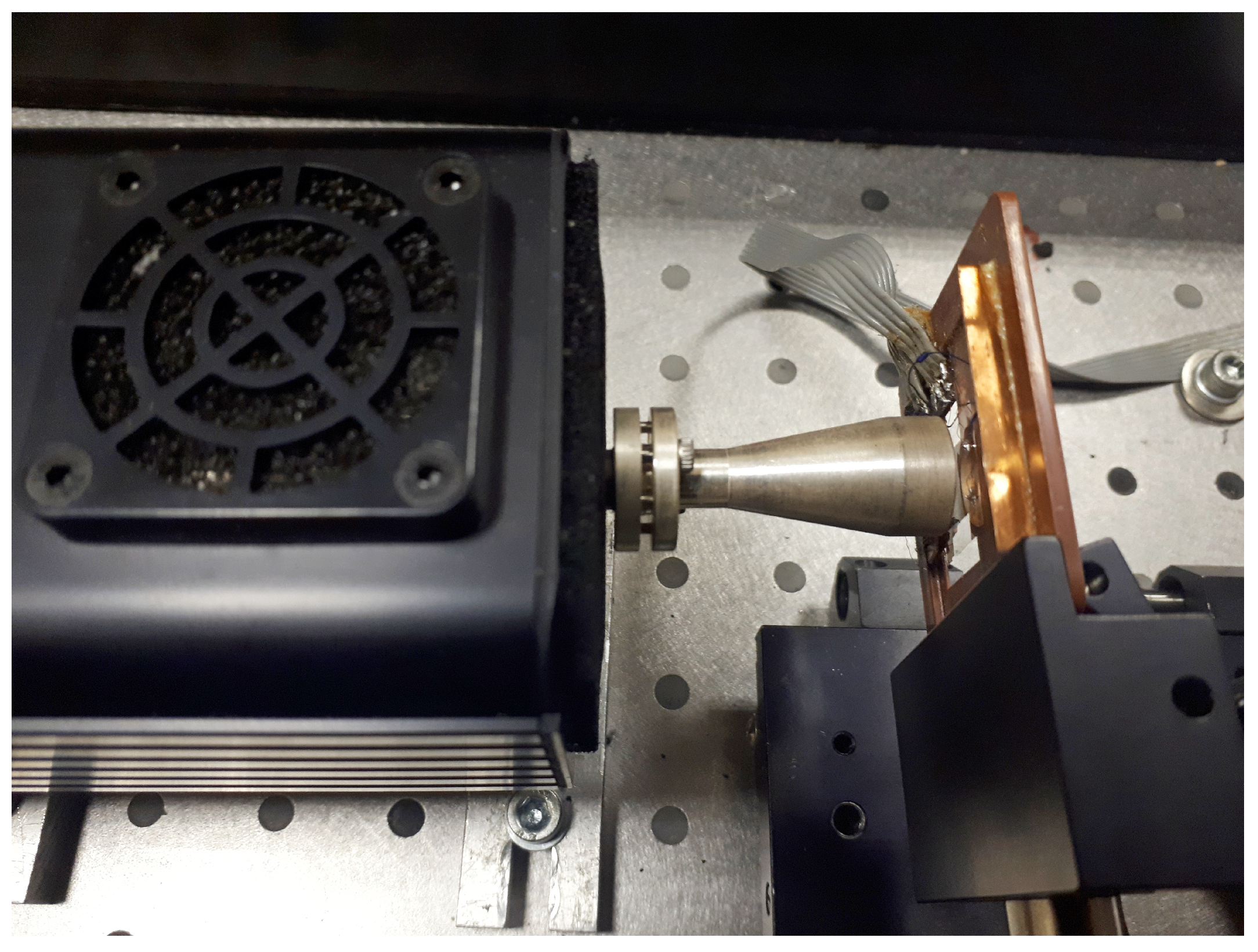
2.1. Experimental Setup

In the experiment, the Terasense 140 GHz source of terahertz radiation (IMPATT diode with a power of 36.8 mW (measured using Gentec-EO THZ9B-BL-DA piroelectric detector), conical horn F-band antenna, gaussian beam shape, divergence angle of 7°, aperture diameter of 10.4 mm, gain of 25 dB) was used [16]. The radiation homogeneity was studied with INO Microxcam-384i camera, which has a pixel size of 35 μm (384 × 288 pixels) and NEP of 26.3 pW × Hz−1/2. Thus, the intensity distribution was obtained, which is approximately uniform. The THz radiation with an intensity of 0.43 mW/mm2 illuminated the entire area of the sample (bismuth-antimony thin film; see Figure 1 and Figure 2) which was attached to copper plates. A Fluke 8840A multi-meter with the resolution of 1 μV was connected to the sample. A 1.5 V galvanic cell was also connected to the sample through a 5 kΩ resistor. The left copper plate was acting as a heater; a heating element was attached to it, as well as a thermocouple, which was used to control the temperature gradient. A Keithley 2001 multi-meter with the resolution of 1 μV was used to measure the thermocouple voltage. The right plate was used to cool the sample to room temperature. The THz radiation power measured behind the structure under study does not exceed 2%. The THz radiation source and the sample were covered by a box with a slot for ventilation of the THz emitter to stabilize the temperature and protect the setup from air flows and background infrared radiation. Thus, three types of influence were applied to thin bismuth-antimony film: THz radiation, direct current, and temperature gradient.

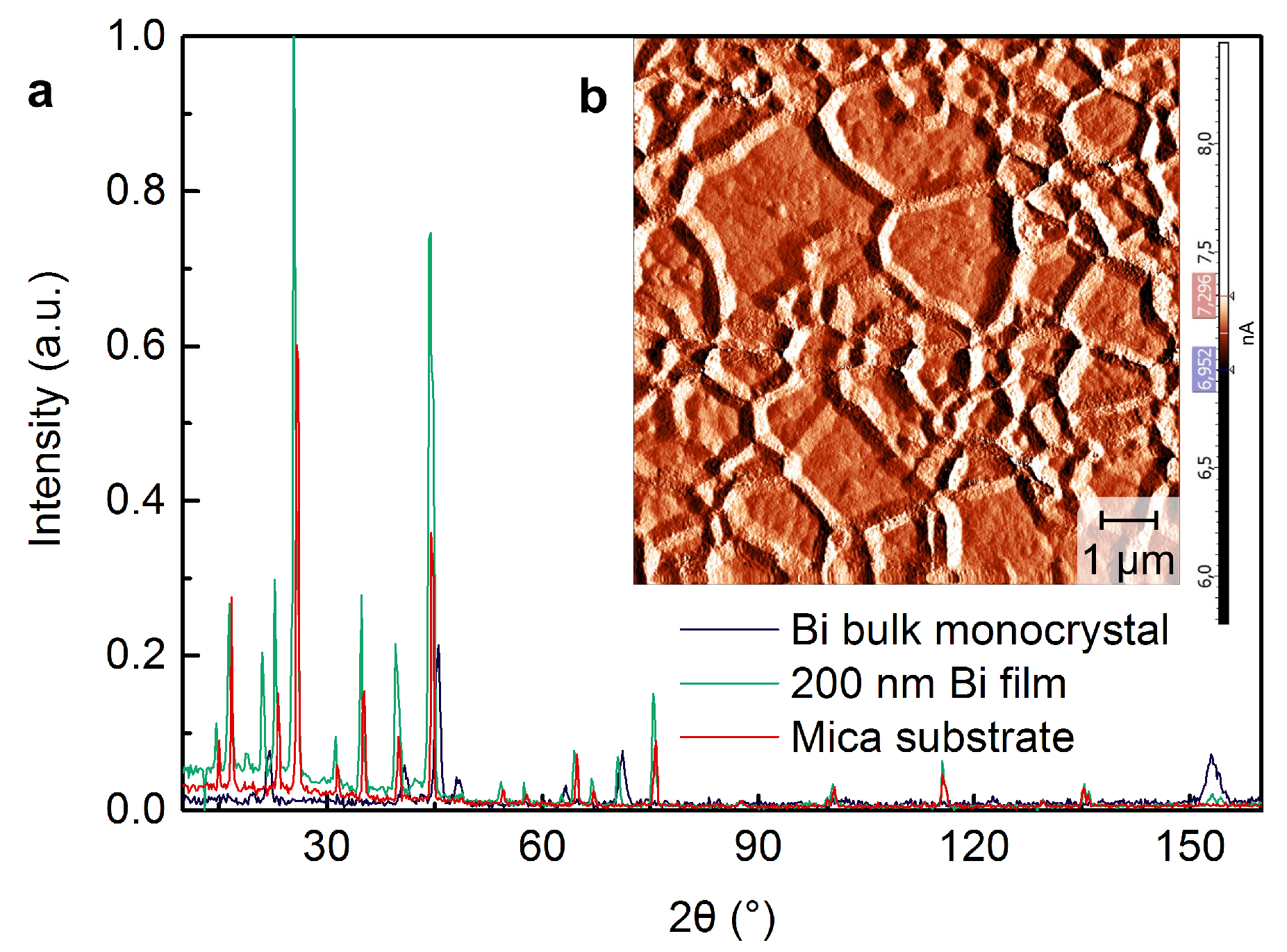
2.2. Bi1−xSbx Synthesis and Characterization

As the samples under study, thin-film Bi1−xSbx solid solutions (intrinsic semimetals) on 21 μm mica substrate were used. To obtain these films, the method of thermal evaporation in vacuum was used. This method consists in the evaporation of the substance located on the evaporator, and the subsequent condensation of the substance on the substrate. To obtain a film of homogeneous composition throughout the volume, the method of discrete evaporation was used. The substance of the desired composition was poured in portions into the evaporator, which made it possible to obtain a film of uniform composition. The film was formed in vacuum at a pressure of 10 5 Torr, the substrate temperature was maintained at 120 °C during the deposition of the substance. Annealing was then carried out at a temperature of 200 °C for 30 min. As a result, 200 nm Bi1−xSbx films were obtained with antimony concentration x of 3%, 8%, and 12%. Their thickness was controlled with Linnik’s interferometry (the measurement error does not exceed 5 nm). If the film thickness differed from the target value (200 nm) by more than 5 nm, it was replaced with another one with the correct thickness. The chemical composition (antimony concentration x) was controlled using X-ray fluorescence analysis (with an accuracy of 0.05%). The materials used to create a solid Bi-Sb solution had a chemical purity of 99.99%.
The X-ray diffraction (XRD) patterns and atomic force microscopy (AFM) image are presented in Figure 3. They allow to estimate the quality and the crystallographic orientation of the synthesized Bi1−xSbx film. The composition of the film is uniform, which is due to the use of one of the most reliable synthesis technologies (thermal evaporation). From the point of view of transport phenomena, the film is a block bicrystal in the plane. In the perpendicular direction, the film can be considered a single crystal. The roughness of the film is no more than 30 nm (single chilocks), which insignificantly influences the effects under study, since the main interaction with radiation occurs in a volume of the film.

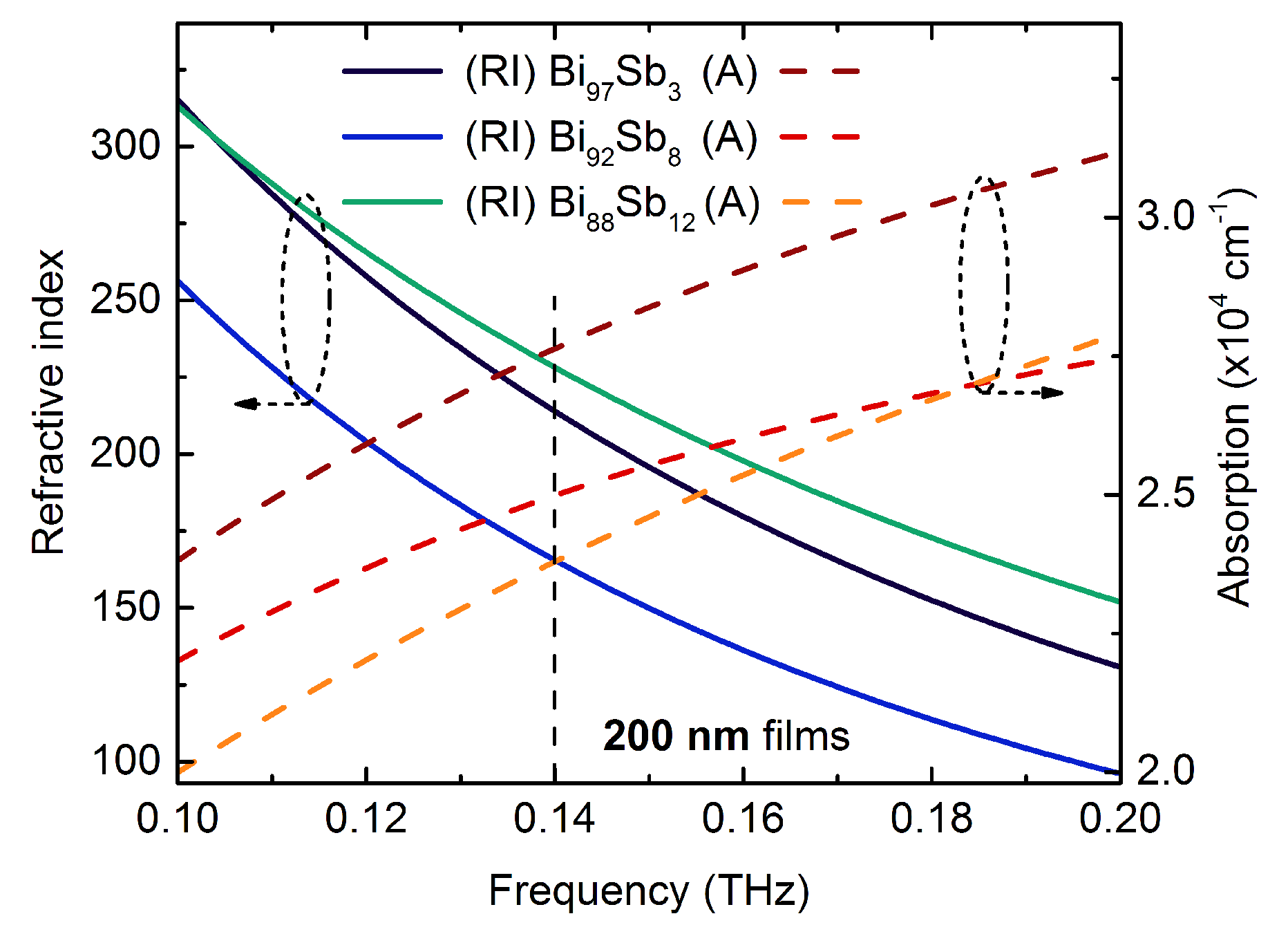
2.3. Optical Properties of Bi1−xSbx Films
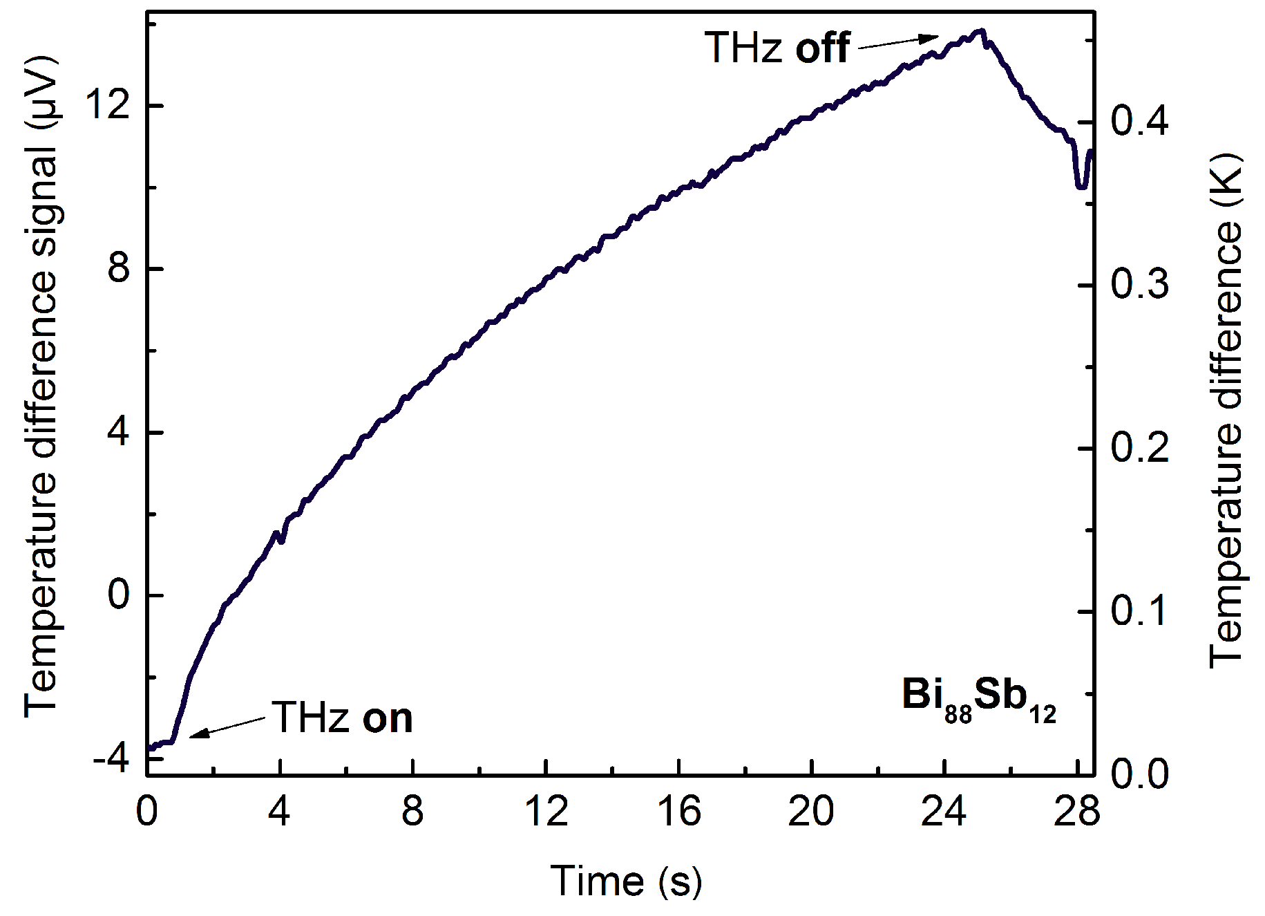
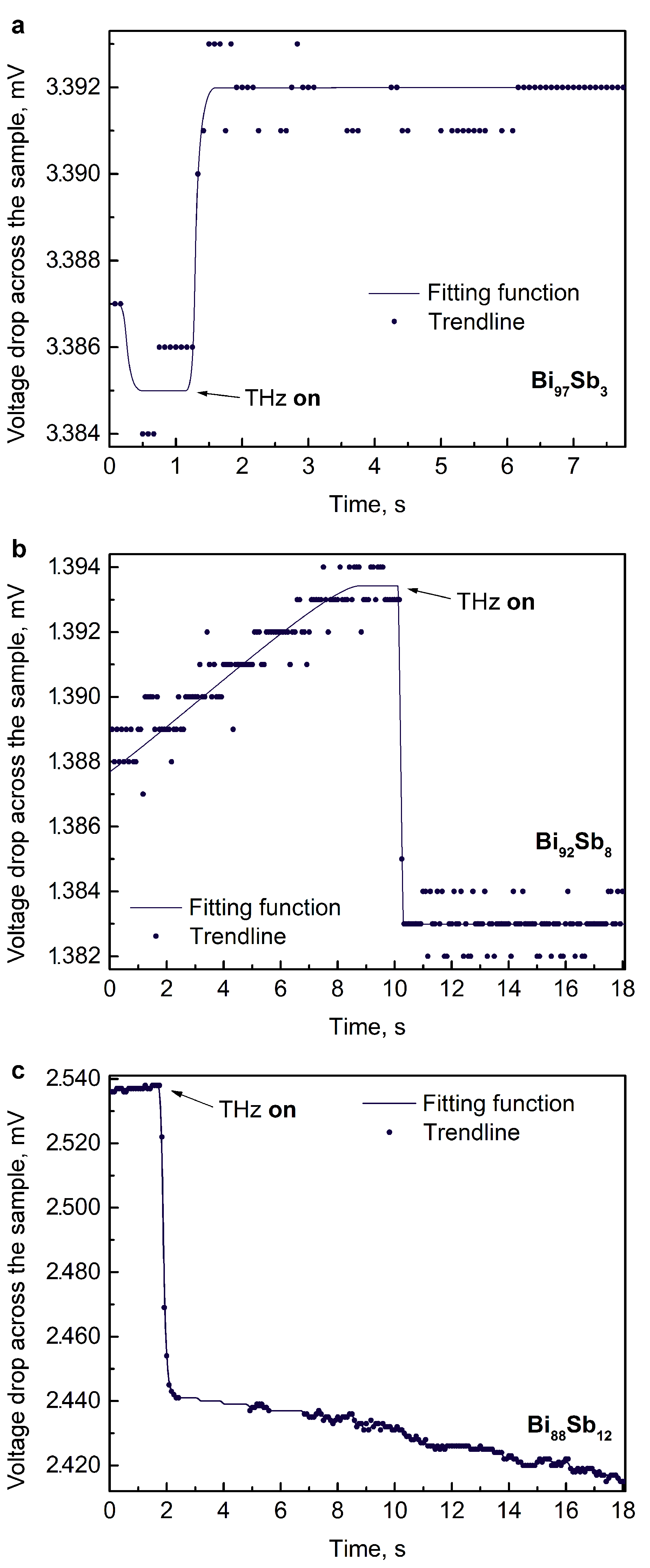
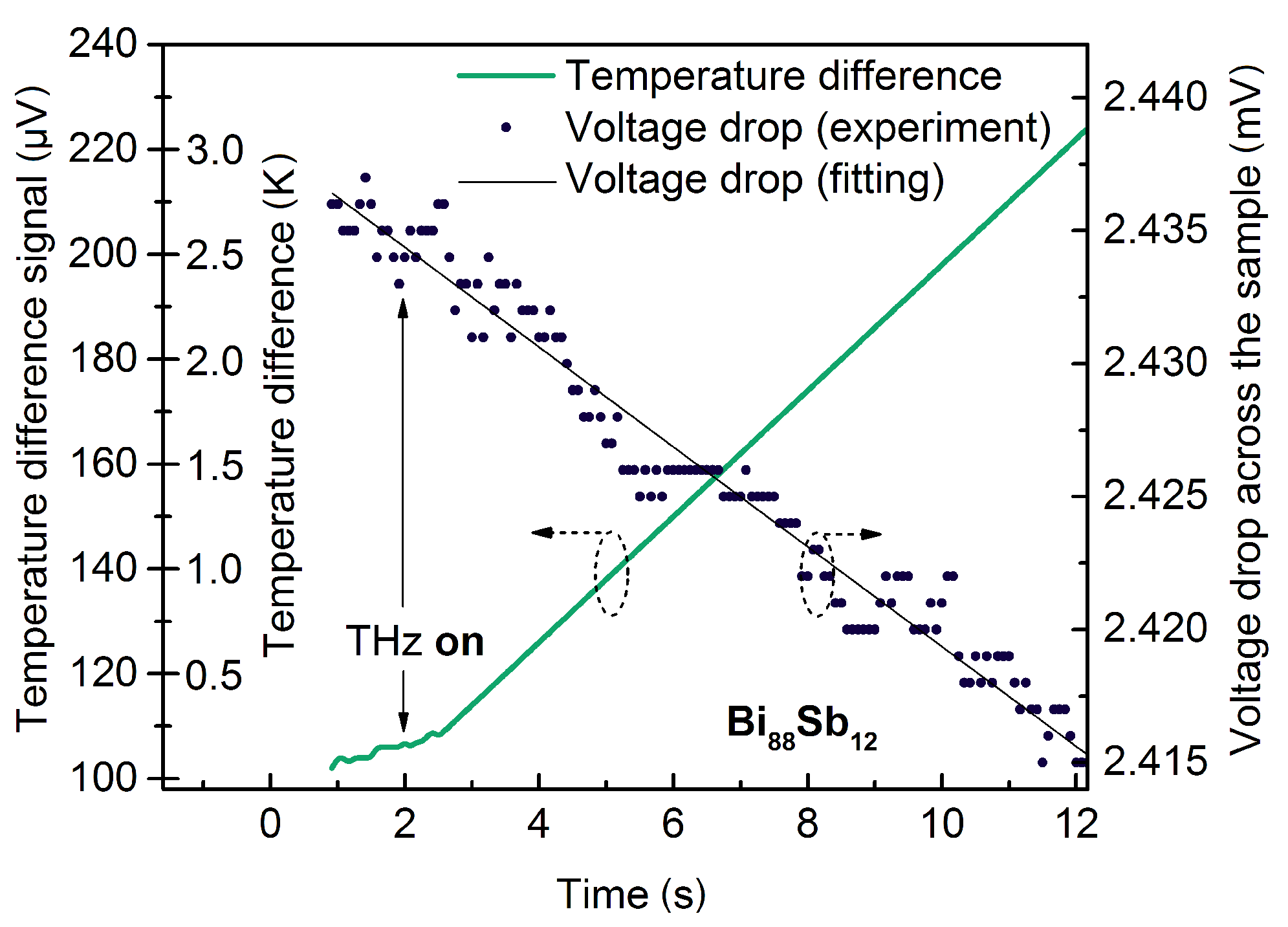
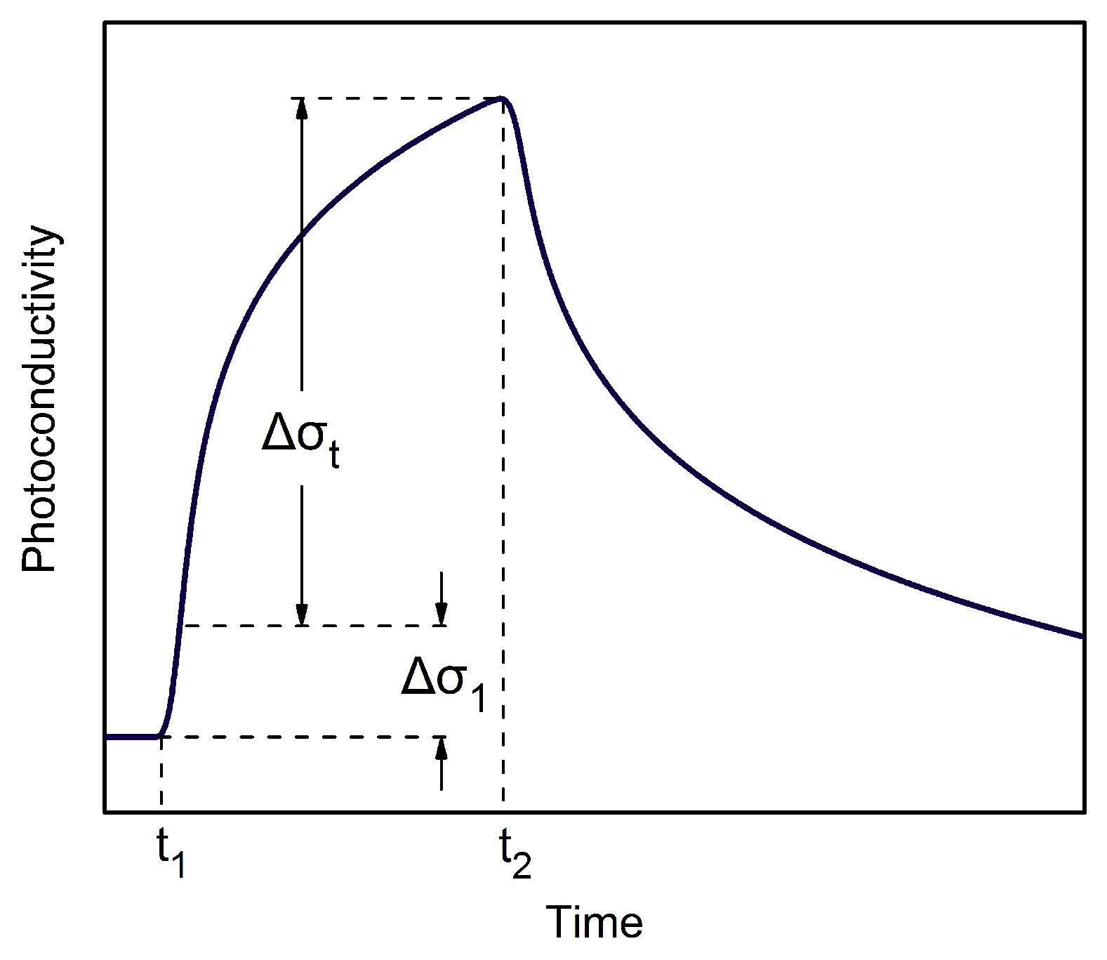
The properties of Bi1−xSbx films were studied in the frequency range of 0.1–0.2 THz by means of terahertz time-domain spectroscopy based on InAs THz generator irradiated by an infrared femtosecond laser (1040 nm, 200 fs, 70 MHz, 15 nJ) in the previous work for 70 nm and 150 nm films [17]. These studies were performed at a temperature of 290 K. The THz waveforms passed through the air, the bare mica substrate and the film-on-substrate structures were recorded and then were used to calculate the corresponding spectra of complex electric field amplitudes (amplitudes and phases) using the fast Fourier transformation.
The further calculations require the extraction of the mica substrate complex effective refractive index spectrum:
n ^ m i c a ( f ) = c [ ϕ m i c a ( f ) ϕ a i r ( f ) ] / ( 2 π f d m i c a ) + 1 i c l n ( | E ^ m i c a ( f ) | 2 / | E ^ a i r ( f ) | 2 ) / ( 4 π f d m i c a ) ,
where f is the THz radiation frequency, c is the speed of light, ϕ m i c a and ϕ a i r are the phases of the bare substrate and air signals, E ^ m i c a and E ^ a i r are the corresponding complex electric field amplitudes, d m i c a is the substrate thickness, and i is the imaginary unit. Then, the complex sheet conductivity of Bi1−xSbx films was calculated in a thin-film approximation (on the basis of Tinkham’s equation) [18]:
σ ^ ( f ) = [ ( n ^ m i c a ( f ) + 1 ) E ^ m i c a ( f ) / E ^ w h o l e ( f ) n ^ m i c a ( f ) 1 ] / Z 0 ,
where Z 0 = 120 π Ohm is the free space impedance, and E ^ w h o l e is the complex electric field amplitude of THz wave passed through the film-on-substrate structure.
The complex sheet conductivity is then used to extract the complex permittivity of Bi1−xSbx films [19]:
ε ^ ( f ) = 1 + i σ ^ ( f ) / ( 2 π f d f i l m ε 0 ) ,
where d f i l m is the film thickness (measured by Linnik’s interferometry), and ε 0 is the permittivity of the free space.
The conductivity/permittivity spectra measured for 70 nm and 150 nm films [17] were well approximated using the classical Drude model. Then, the model parameters were linearly extrapolated to the thickness of 200 nm to obtain the complex permittivity of the films studied in this work. Such an operation should have a low error due to proximity of the investigated thicknesses (70–150–200 nm).
The root of a complex permittivity gives the complex refractive index of a film, which consists of real and imaginary parts responsible for refraction and absorption correspondingly. Through the results of calculations that are presented in Figure 4, it can be seen that refraction index and absorption coefficient strongly depend on a frequency of THz radiation and on Sb concentration. In further calculations, we use the values of these parameters at the only one frequency of 0.14 THz, since the interaction of films with continuous-wave radiation at 0.14 THz is investigated in this work.
The dependence of complex permittivity of a thin film on Sb content is nonlinear: plasma frequency and damping rate may not change in the same way, as well as the effective mass of charge carriers and their mobility. This behavior is due to the strong dependence of the band structure of the material on Sb content [20]. With rising percentage of Sb, the absorption coefficient tends to decrease, while the refractive index first decreases and then increases (has a minimum at 8% Sb).

3. Results

In the first experiment, no current was flowing through the sample, the gradient furnace was switched off, so that the sample was out of electric field and the temperature throughout the sample was the same. During the experiment, temperature gradient was revealed while materials were affected by THz radiation. Temporal dependence of temperature gradient on duration of radiation influence is presented in Figure 5. In case of long exposure with constant power radiation, the temperature gradient kept changing, but with a low rate. Despite absence of thermal gradient and electric field, the signal still could be received. The values of temperature difference signal lie in the range between 4 and 13 μV under these conditions.
In the second experiment, 1.5 mA direct current was flowing through the sample, gradient furnace was switched off; thus, the sample was in the electric field, but the temperature throughout the sample was the same. In Figure 6, there are temporal dependencies for the next compositions: Bi97Sb3, Bi92Sb8, Bi88Sb12. Initially, voltage drop across the sample was measured without radiation. Then, radiation was switched on at the time point designated in Figure 6. After a very short time interval (comparable with voltmeter measurement rates), voltage drop change can be seen. For Bi97Sb3 film (Figure 6a), this effect is not very significant. For approximately 2 s, there was a voltage drop decrease, i.e., conductivity increase, and, afterwards, voltage drop increases, i.e., conductivity decreases. For Bi92Sb8 (Figure 6b) and Bi88Sb12 (Figure 6c) films, the effect had the same direction but different values. During the first seconds of the experiment, voltage drop changes linearly due to thermoelectric effect induced by flowing current. With THz radiation turning on, voltage drop decreases, which means that conductivity increases in these films. In Bi92Sb8 and Bi88Sb12, films the effect is similar to photoconductivity in semiconductors.
The investigated effects appear most noticeably in Bi88Sb12 sample, and they are important from the point of view of obtaining the highest detection efficiency of THz radiation.
Each measurement was repeated three times to confirm the accuracy of the results obtained. The differences in the behavior of the curves in Figure 6 for solid solutions with different concentrations of antimony are associated with differences in the band structure of the material [20]. For Bi97Sb3 film on mica substrate, an overlap of the valence and conduction bands is observed in the material at a room temperature, while a gap is observed in the case of a higher antimony concentration (Bi92Sb8 and Bi88Sb12). Additional charge carriers may reduce the conductivity of the material in the case of Bi97Sb3. It should be mentioned that vertical axis steps in Figure 6 are caused by digitization associated with the resolution of the multi-meter.
In the third experiment, no current was flowing through the sample; thus, the sample was out of electric field; gradient furnace was turned on, so the temperature heterogeneity was created. With THz radiation turning on, gradient began changing. This effect is demonstrated in (Figure 7). Consequently, this thermal effect is related with interaction between radiation and the film or the substrate lattice. The temperature gradient allows to increase the sensor sensitivity in the case of Bi88Sb12.

4. Discussion

The electron-hole pairs are formed during to interaction with radiation. Therefore, bismuth-antimony can be considered as a material with traps, and radiation increases their number. To explain the data from the second experiment, a theory for semiconductors [21] may be used.
A typical curve of increase and decrease in photoconductivity for crystal with traps is demonstrated schematically in Figure 8. Charge carrier concentration increases during the time period defined by the recombination time. Due to excess electron and hole concentration, the conductivity increases by
Δ σ 1 = q μ e δ n e + q μ p δ n p ,
where δ n e and δ n p are an electron and a hole concentration increment correspondingly, μ e and μ p are an electron and a hole mobility, and q is the electron charge.
Excess concentration of electrons increases the rate of capture by the traps, and the traps are gradually filled. The filling rate of the traps can be changed by changing the excitation light intensity.
The electrons caught by the traps are not involved in charge transport. However, to neutralize trapped electrons charge, excess hole concentration is required. This increases conductivity by (see Figure 8)
Δ σ t = q μ p n t ,
where n t is a concentration of additional charge carriers.
The concentration of trapped electrons and excess conductivity decrease with excitation beam shutdown as it shown in Figure 8. To define the lifetime of unbalanced charge carriers, photoconductivity increase and decrease curves are often used. In the presence of traps, the time constants characterize their filling or release.
Using this theory, the added conductivity can be defined as conductivity decrease by e times in Figure 6. The results of calculations are presented in Table 1 (added conductivity, Δ σ t ).
The frequency dependencies of refractive index and absorption coefficient were demonstrated in Figure 4, and the values are represented in Table 1 for 0.14 THz. Absorption coefficient dependency on absolute conductivity (stationary( σ 0 ) + photoconductivity ( Δ σ 1 + Δ σ t )) and frequency can be evaluated as
α = 2 ω k c = σ c n ε 0 1 + τ ω 2 ,
where ω = 2 π ν is an angular frequency of THz radiation, k is an extinction (absorption) coefficient, c is the speed of light in vacuum, σ is a conductivity, n is a refractive index, ε 0 is the vacuum permittivity, and τ is the relaxation time (see Table 1) which was previously estimated for the same samples in Reference [17].
During the experiments, current and voltage drop values in the film were measured. Hence, conductivity value can be defined for samples under radiation influence and without applying radiation.
Calculation of conductance G was performed using Ohm’s law:
G = I U ,
where I is current, and U is voltage taken from experiment. The time-dependent conductance was then analyzed on the basis of the model described in Figure 8. We used Equations (2) and 3 to calculate the value of additional charge carriers. Value of the charge carriers has been defined as
n p = α · c n ε 0 1 + τ ω 2 q · μ p .
Bismuth-antimony solid solutions may have the topological insulating properties under certain conditions, when they are characterized with a narrow bandgap [23]. However, the band structure of thin-film solid Bi1−xSbx solution and corresponding properties (like resistivity) strongly depend on Sb content [20], temperature and film thickness [23], and even substrate material [20]. In our manuscript, the presence of this effect has not been examined, since it does not affect the interaction of the medium with THz radiation and the efficiency of its detection. This is due to the fact that the skin depth at a given frequency of 0.14 THz significantly exceeds the thickness of the surface layer, which, as a rule, has a thickness of several nm and in which the effect of topological insulation can potentially be observed.

5. Conclusions

The temporal dependencies of a voltage drop and a temperature gradient across the sample were studied under influence of THz radiation and direct current. The results of experiments demonstrate two effects of radiation influence. There are different temporal dependencies of intensity for each effect. For instance, thermal impact can be used for precise power calibration. The second effect, that consists in impact on electron spectrum, i.e., conductivity, can be used to detect the presence of radiation.
For practical purposes, THz detectors that operate at room temperature are most convenient. Such devices include Golay cells [24], thin-film pyroelectric sensors [25], Schottky diodes [26], and field-effect transistors [27]. The log-periodic circular-toothed antenna-coupled bilayer graphene field-effect transistor (GFET) THz detector has sensitivity up to ∼150 mV·W−1 at 0.3 THz and modulation frequency of 500 Hz [27]. The log-periodic broadband planar antenna-coupled Si junctionless FET (JLFET) detector has sensitivity up to ∼500 mV·W−1 at 0.18 THz and modulation frequency of 187 Hz [28]. The on-chip cross-dipole antenna-coupled thermal CMOS THz detector has sensitivity up to ∼6000 mV·W−1 at 0.8 THz [29]. The integrated split bow-tie antenna-coupled top-gated CVD graphene field-effect transistor (GFET) THz detector has sensitivity up to ∼14,000 mV·W−1 at 0.6 THz and modulation frequency of 333 Hz [30].
The sensitivity of this Bi1−xSbx detector without using a chopper and antenna is up to ∼3000 mV·W−1 at 0.1 THz. The practically achievable time resolution/response speed of such THz detectors is RC-limited by the design of the electric circuitry and by the bandwidth of cables and amplifiers. THz detector based on Bi1−xSbx thin films is a very promising compact, low-cost, frequency broadband alternative with tunable voltage responsivity to above-mentioned devices utilized for THz detection. Such Bi1−xSbx detectors can be integrated to multipixel detector arrays, which allows for a compact cost-efficient layout of THz imaging systems.
The measurements were performed at a single frequency of 0.14 THz; therefore, there remains a large amount of work related to the study of the detection efficiency of broadband terahertz radiation or radiation at other single frequencies. The question remains open related to the power threshold, after which nonlinear effects begin to appear. The possibility of determining the frequency of THz radiation using the materials presented in this work is also a serious subject for future investigations, as well as measuring the maximum possible modulation frequency of THz radiation. It is important to note that a significant increase in the efficiency of the detection system can be achieved through the use of synchronous amplification of the THz signal during its modulation.

Author Contributions

Conceptualization, M.K.K., N.S.K.; methodology, M.K.K., N.S.K., P.S.D., E.S.M.;formal analysis, N.S.K., I.L.T.; investigation, N.S.K., E.S.M., P.S.D., D.V.Z.; data curation, P.S.D., D.V.Z., E.S.M., I.L.T., A.S.T., A.V.A., A.V.N.; writing–original draft preparation, N.S.K., I.L.T., M.K.K., A.D.Z.; writing–review and editing, M.K.K., N.S.K.; visualization, N.S.K., P.S.D., A.D.Z.; supervision, M.K.K.; funding acquisition, M.K.K. All authors have read and agreed to the published version of the manuscript.

Funding

This research was funded by Russian Science Foundation, grant number 19-72-10141.

Conflicts of Interest

The authors declare no conflict of interest. The funders had no role in the design of the study; in the collection, analyses, or interpretation of data; in the writing of the manuscript, or in the decision to publish the results.

References

  1. Dexheimer, S.L. Terahertz Spectroscopy: Principles and Applications; CRC Press: Boca Raton, FL, USA, 2017. [Google Scholar]
  2. Malhotra, I.; Jha, K.R.; Singh, G. Terahertz antenna technology for imaging applications: A technical review. Int. J. Microw. Wirel. Technol. 2018, 10, 271. [Google Scholar] [CrossRef]
  3. Chan, W.L.; Deibel, J.; Mittleman, D.M. Imaging with terahertz radiation. Rep. Prog. Phys. 2007, 70, 1325. [Google Scholar] [CrossRef]
  4. Choi, H.; Son, J.H.; Son, J.H. Terahertz imaging and tomography techniques. In Terahertz Biomedical Science and Technology; CRC Press: Boca Raton, FL, USA, 2014; pp. 47–66. [Google Scholar]
  5. Yang, X.; Zhao, X.; Yang, K.; Liu, Y.; Liu, Y.; Fu, W.; Luo, Y. Biomedical applications of terahertz spectroscopy and imaging. Trends Biotechnol. 2016, 34, 810–824. [Google Scholar] [CrossRef]
  6. Zaytsev, K.I.; Kudrin, K.G.; Koroleva, S.A.; Fokina, I.N.; Volodarskaya, S.I.; Novitskaya, E.V.; Perov, A.N.; Karasik, V.E.; Yurchenko, S.O. Medical diagnostics using terahertz pulsed spectroscopy. In Journal of Physics: Conference Series; IOP Publishing: Bristol, England, 2014; Volume 486, p. 012014. [Google Scholar]
  7. Kato, M.; Tripathi, S.R.; Murate, K.; Imayama, K.; Kawase, K. Non-destructive drug inspection in covering materials using a terahertz spectral imaging system with injection-seeded terahertz parametric generation and detection. Opt. Express 2016, 24, 6425–6432. [Google Scholar] [CrossRef]
  8. Ospald, F.; Zouaghi, W.; Beigang, R.; Matheis, C.; Jonuscheit, J.; Recur, B.; Guillet, J.P.; Mounaix, P.; Vleugels, W.; Bosom, P.V.; et al. Aeronautics composite material inspection with a terahertz time-domain spectroscopy system. Opt. Eng. 2013, 53, 031208. [Google Scholar] [CrossRef]
  9. Nagatsuma, T.; Ducournau, G.; Renaud, C.C. Advances in terahertz communications accelerated by photonics. Nat. Photonics 2016, 10, 371–379. [Google Scholar] [CrossRef]
  10. Sizov, F. Terahertz radiation detectors: The state-of-the-art. Semicond. Sci. Technol. 2018, 33, 123001. [Google Scholar] [CrossRef]
  11. Lewis, R.A. A review of terahertz detectors. J. Phys. Appl. Phys. 2019, 52, 433001. [Google Scholar] [CrossRef]
  12. Markov, M.; Rezaei, S.E.; Sadeghi, S.N.; Esfarjani, K.; Zebarjadi, M. Thermoelectric properties of semimetals. Phys. Rev. Mater. 2019, 3, 095401. [Google Scholar] [CrossRef] [Green Version]
  13. Rowe, D.M. CRC Handbook of Thermoelectrics; CRC Press: Boca Raton, FL, USA, 2018. [Google Scholar]
  14. Lu, X.; Sun, L.; Jiang, P.; Bao, X. Progress of photodetectors based on the photothermoelectric effect. Adv. Mater. 2019, 31, 1902044. [Google Scholar] [CrossRef]
  15. Cai, X.; Sushkov, A.B.; Suess, R.J.; Jadidi, M.M.; Jenkins, G.S.; Nyakiti, L.O.; Myers-Ward, R.L.; Li, S.; Yan, J.; Gaskill, D.K.; et al. Sensitive room-temperature terahertz detection via the photothermoelectric effect in graphene. Nat. Nanotechnol. 2014, 9, 814. [Google Scholar] [CrossRef] [Green Version]
  16. Terahertz Sources. Available online: http://terasense.com/products/terahertz-sources (accessed on 10 March 2021).
  17. Zaitsev, A.D.; Demchenko, P.S.; Zykov, D.V.; Korotina, E.A.; Makarova, E.S.; Tkhorzhevskiy, I.L.; Tukmakova, A.S.; Kablukova, N.S.; Asach, A.V.; Novotelnova, A.V.; et al. Optical and Galvanomagnetic Properties of Bi1-xSbx Thin Films in the Terahertz Frequency Range. Appl. Sci. 2020, 10, 2724. [Google Scholar] [CrossRef] [Green Version]
  18. Tinkham, M. Energy gap interpretation of experiments on infrared transmission through superconducting films. Phys. Rev. 1956, 104, 845. [Google Scholar] [CrossRef]
  19. Novotny, L.; Hecht, B. Principles of Nano-Optics; Cambridge University Press: Cambridge, UK, 2012. [Google Scholar]
  20. Suslov, A.; Grabov, V.; Komarov, V.; Demidov, E.; Senkevich, S.; Suslov, M. The Band-Structure Parameters of Bi 1–x Sb x (0 ≤ x ≤ 0.15) Thin Films on Substrates with Different Thermal-Expansion Coefficients. Semiconductors 2019, 53, 611–614. [Google Scholar] [CrossRef]
  21. Sahu, M.K. Semiconductor nanoparticles theory and applications. Int. J. Appl. Eng. Res. 2019, 14, 491–494. [Google Scholar]
  22. Suslov, A.; Komarov, V.; Suslov, M. Galvanomagnetic properties of Bi85Sb15 thin films on glass and glass-ceramic substrates. In Materials Science and Condensed Matter Physics; Institute of Applied Physics: Kishinev, Moldova, 2016; p. 245. [Google Scholar]
  23. Demidov, E.; Grabov, V.; Komarov, V.; Kablukova, N.; Krushel’nitskii, A. Topological insulator state in thin bismuth films subjected to plane tensile strain. Phys. Solid State 2018, 60, 457–460. [Google Scholar] [CrossRef]
  24. TYDEX. Available online: http://tydex.ru (accessed on 10 March 2021).
  25. Müller, R.; Gutschwager, B.; Hollandt, J.; Kehrt, M.; Monte, C.; Müller, R.; Steiger, A. Characterization of a large-area pyroelectric detector from 300 GHz to 30 THz. J. Infrared Millim. Terahertz Waves 2015, 36, 654–661. [Google Scholar] [CrossRef] [Green Version]
  26. Virginia Diodes. Available online: http://vadiodes.com (accessed on 10 March 2021).
  27. Vicarelli, L.; Vitiello, M.; Coquillat, D.; Lombardo, A.; Ferrari, A.C.; Knap, W.; Polini, M.; Pellegrini, V.; Tredicucci, A. Graphene field-effect transistors as room-temperature terahertz detectors. Nat. Mater. 2012, 11, 865–871. [Google Scholar] [CrossRef] [PubMed]
  28. Zagrajek, P.; Danilov, S.N.; Marczewski, J.; Zaborowski, M.; Kolacinski, C.; Obrebski, D.; Kopyt, P.; Salski, B.; But, D.; Knap, W.; et al. Time resolution and dynamic range of field-effect transistor–based terahertz detectors. J. Infrared Millim. Terahertz Waves 2019, 40, 703–719. [Google Scholar] [CrossRef] [Green Version]
  29. Chen, F.; Yang, J.; Li, Z. Modeling of an uncooled CMOS THz thermal detector with frequency-selective cross-dipole antenna and NMOS temperature sensor. Microw. Opt. Technol. Lett. 2017, 59, 3160–3166. [Google Scholar] [CrossRef]
  30. Zak, A.; Andersson, M.A.; Bauer, M.; Matukas, J.; Lisauskas, A.; Roskos, H.G.; Stake, J. Antenna-integrated 0.6 THz FET direct detectors based on CVD graphene. Nano Lett. 2014, 14, 5834–5838. [Google Scholar] [CrossRef] [PubMed]
Figure 1. Schematic view of the experimental configuration.
Photonics 08 00076 g001
Figure 2. Photo of the experimental setup. The Terasense 140 GHz source of terahertz radiation illuminates the entire area of the sample to which the control devices and parameter reading devices are connected with a plume.
Photonics 08 00076 g002
Figure 3. (a) X-ray diffraction (XRD) patterns for Bi(111) bulk monocrystal, 200 nm Bi film, and mica substrate. The bifurcated peak at 153° indicates the (111) film plane crystallographic orientation. (b) Atomic force microscopy (AFM) image of a 200 nm Bi film surface.
Photonics 08 00076 g003
Figure 4. Refractive index (solid lines) and absorption coefficient (dashed lines) dispersions of 200 nm Bi1−xSbx films in 0.1–0.2 THz frequency range for various Sb concentrations [17]. The vertical line at 0.14 THz represents the frequency point for parameters values used in further calculations.
Photonics 08 00076 g004
Figure 5. First experiment (photothermal effect). The temporal dependence of a temperature gradient in 200 nm Bi88Sb12 film on the terahertz (THz) field exposure time.
Photonics 08 00076 g005
Figure 6. Second experiment (photoelectric effect). The temporal dependencies of voltage in 200 nm Bi97Sb3 (a), Bi92Sb8 (b), Bi88Sb12 (c) films under the influence of direct current and THz radiation.
Photonics 08 00076 g006
Figure 7. Third experiment (photothermoelectric effect).The temporal dependence of voltage drop in 200 nm Bi88Sb12 films under the influence of THz radiation.
Photonics 08 00076 g007
Figure 8. The typical temporal dependence of increase and decrease in photoconductivity for a crystal with traps under influence of radiation.
Photonics 08 00076 g008
Table 1. Extracted material data.
Quantity3%8%12%
Conductivity [17] σ 0 , (Ohm·m)−12.21 × 10 6 5.38 × 10 6 2.96 × 10 6
Added conductivity Δ σ t 0.0012 σ 0 0.0043 σ 0 0.0217 σ 0
Stationary photo-conductivity Δ σ 1 0.0027 σ 0 0.0029 σ 0 0.0236 σ 0
Refractive index [17] n214166228
Absorption coefficient [17] α , cm−1 2.76 × 10 4 2.50 × 10 4 2.38 × 10 4
Stationary carrier concentration [22] n e s , m−3 1.8 × 10 24 1.7 × 10 24 2.0 × 10 24
Electron mobility [22] μ e , m2/(V·s)4.12.43.2
Hole mobility [22] μ p , m2/(V·s)0.80.270.18
Relaxation time [17] τ , ps0.3710.3420.335
Carrier concentration under THz radiation n p , m−31.38 × 10 25 2.86 × 10 25 5.20 × 10 25
n p / n e s 7.6716.8125.99
Publisher’s Note: MDPI stays neutral with regard to jurisdictional claims in published maps and institutional affiliations.

