Communication

Photonic Nanojet Generation Using Integrated Silicon Photonic Chip with Hemispherical Structures

by
Aneesh Vincent Veluthandath
and
Ganapathy Senthil Murugan
*
Optoelectronics Research Centre, University of Southampton, Southampton SO17 1BJ, UK
*
Author to whom correspondence should be addressed.
Photonics 2021, 8(12), 586; https://doi.org/10.3390/photonics8120586
Submission received: 30 November 2021 / Revised: 11 December 2021 / Accepted: 15 December 2021 / Published: 17 December 2021
(This article belongs to the Section Optoelectronics and Optical Materials)

Abstract

:
Photonic nanojet (PNJ) is a tightly focused diffractionless travelling beam generated by dielectric microparticles. The location of the PNJ depends on the refractive index of the material and it usually recedes to the interior of the microparticle when the refractive index is higher than 2, making high index materials unsuitable to produce useful PNJs while high index favours narrower PNJs. Here we demonstrate a design of CMOS compatible high index on-chip photonic nanojet based on silicon. The proposed design consists of a silicon hemisphere on a silicon substrate. The PNJs generated can be tuned by changing the radius and sphericity of the hemisphere. Oblate spheroids generate PNJs further away from the refracting surface and the PNJ length exceeds 17 λ when the sphericity of the spheroid is 2.25 The proposed device can have potential applications in focal plane arrays, enhanced Raman spectroscopy, and optofluidic chips.

Graphical Abstract

1. Introduction

Photonic nanojet (PNJ) is a tightly focused travelling beam of light that is generated at the shadow side of a dielectric microparticle illuminated with a plane wave [1,2]. It is a non-evanescent, non-resonant, travelling wave phenomenon. PNJ was first observed by Chen et al. in a computational study of light scattering by infinite cylinders [1]. The PNJ offers subwavelength light confinement for distances of the order of a few wavelengths. The strong electromagnetic field enhancement and the narrow beam width for PNJs, for relatively long distances, offer many practical applications. PNJs are used to enhance Raman scattering [3,4] and for the enhancement of light scattering by nanoparticles [1,5]. PNJ-driven nonlinear optical phenomena such as two photon fluorescence [6] and all optical switching [7] were also demonstrated. One of the important applications of PNJ is in microscopy, where it is used to enhance the resolution. Using a PNJ with waist less than the diffraction limit, it is possible to enhance the resolution of the microscope. A resolution of λ / 4 , higher than the Rayleigh limit, was demonstrated by Yang et al. [8]. The resolution was further improved to λ / 12 by Bintao et al. [9]. Another interesting application, coupled resonator optical waveguiding, was also demonstrated using microspheres that support PNJs [10]. The subwavelength beam width has been successfully employed to improve the resolution of lithography [11,12]. The earliest work on PNJ-assisted lithography used an array of dielectric microspheres to create micropillar and hole patterns on photoresists [13]. Jacassi et al. mounted the microsphere on an AFM cantilever to write arbitrary patterns on a photoresist [12]. Another important application is nanoparticle detection and tracking. Yang et al. has shown that an array of PNJs integrated into a microfluidic chip can track the movements of nanoparticles [14]. Another interesting application of PNJ is its use as optical tweezer [15]. Optical trapping and detection of nanoparticles and cells using PNJ array has also been demonstrated by Li et al. [16].
The PNJs are characterized by their length ( L P N J ) , the full width at half maximum (FWHM) of the beam waist, and electric field enhancement. These properties are dependent on both size and refractive index of the microparticle ( n )   and the surrounding medium n m [1,17]. Both the length and beam waist of the PNJ increase with increase in the size of the microparticle [17]. The beam FWHM of PNJ decreases with increase in refractive index [17] which in turn increases the field enhancement by the PNJ. Many of the applications of PNJ rely on the high field enhancement and narrow beam waist; therefore, it is desirable to use a high refractive index material for generating PNJ [17]. However, with increase in refractive index, the length of the PNJ shortens and it move towards the surface of microparticle and finally gets embedded inside the particle when the refractive index is higher than 2 [1,17]. Therefore, most of the current applications of PNJs rely on materials with refractive index less than 2 [18].
Many CMOS compatible materials such as silicon (Si) have a refractive index above 2. Therefore, PNJ generated using these materials can provide higher field enhancement and smaller width. However, the PNJ produced by Si spheres and cylinders occur at the interior of the particle/structure and therefore is not useful in practical applications. Multiple attempts were made to sidestep the refractive index limit of 2 [17]. Earlier attempts rely on cleaving or shrinking the spherical or cylindrical structures to push the PNJs to the exterior. Gu et al. designed a geometry consisting of an edge cut length reduced microcylinder of refractive index 2.5. Their length reduced microcylinder was able to generate narrow PNJ outside the particle. Pacheco-Peña studied the PNJ formation in a high refractive index microsphere cleaved to expose the PNJ [19]. A high refractive index cylinder cleaved to expose the PNJ was investigated by Zhen et al. [20]. Geints et al. showed that PNJ can be generated using a high refractive index particle by illuminating the particle in reflection mode [21].
Integrating PNJ into Si is challenging because (a) on-chip integration of the symmetric particles such as spheres and cylinders is difficult and often requires micromanipulation of the particle to place accurately, and (b) due to the high refractive index of the Si, the PNJ of Si spheres and cylinders are generated inside those particles. Recent numerical studies have shown that flat-ended cylinders [22] and two-layer cleaved microcylinders [20] can support PNJ outside the material even if the refractive index is similar to that of Si. However, these structures are difficult to fabricate and integrate onto a CMOS-compatible platform especially when working in visible and near IR wavelengths. They are also difficult to align and handle. Here we demonstrate an on-chip PNJ using silicon, which is the most appropriate device platform for most of the applications mentioned above. Due to the simplicity of design, it can be fabricated using standardized silicon micro-/nano-fabrication techniques [23,24] and the structure can be easily aligned in any optical setup and PNJs can be excited using plane waves.

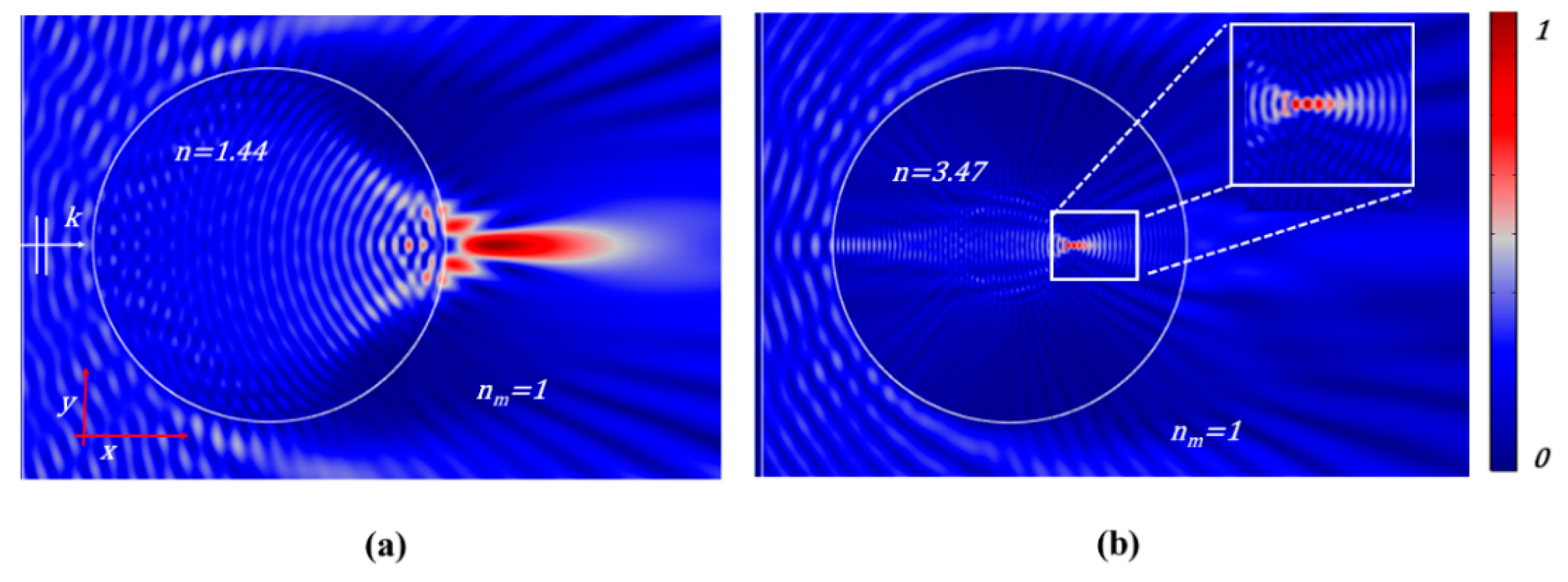
2. Modelling of Photonic Nanojet

The finite element method (FEM) was used to simulate the PNJ. A commercially available FEM package (Comsol Multiphysics) was used in this study. In these simulations, the simulated structures were illuminated by a plane wave of wavelength 1550 nm from the left side of the simulation domain. The 1550 nm wavelength was chosen because silicon is transparent at this wavelength and lasers and other optical components are widely available. The excitation wavelength was kept constant throughout this study. Perfectly matched layer (PML) was applied at external boundaries of the simulation domain. A mesh size of λ / 20 was used in the air domains and λ / ( 3.4 × 20 ) in silica/silicon domains. Figure 1a,b show the distribution of normalized electric filed intensity of PNJs in a silica ( n = 1.44 ) and silicon ( n = 3.47 ) microspheres of radius 5 λ in vacuum ( n m = 1 ), respectively. For the silica microsphere (Figure 1a), a strong PNJ was formed at the exterior of the microsphere which can be used in many applications including imaging [8] and lithography [12]. In the case of silicon microsphere (Figure 1b), PNJ had a much smaller width and higher local electric field intensity. However, it is generated at the interior of the silicon microsphere, making it not useful for any practical applications.

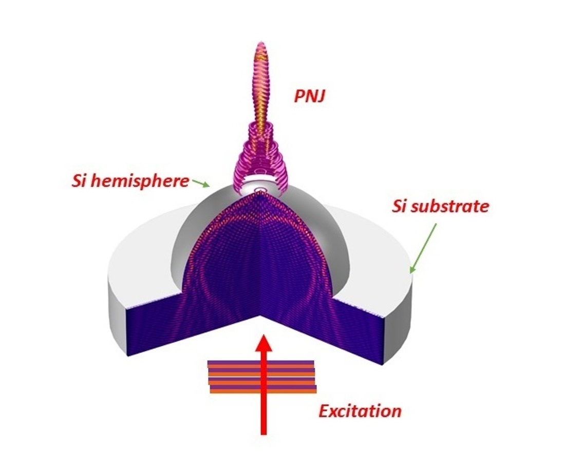
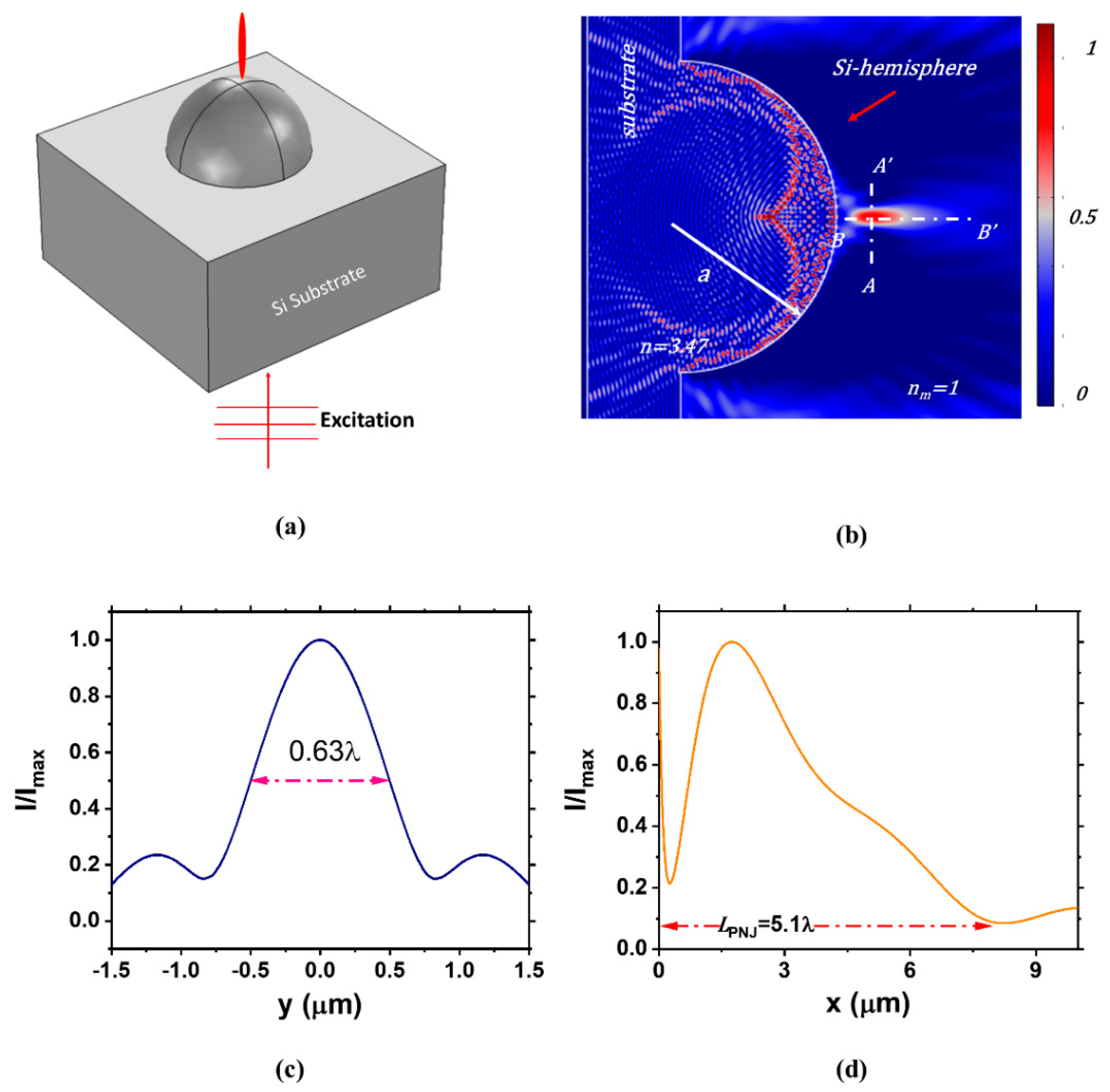
3. On-Chip Photonic Nanojet

Earlier work on PNJ on high refractive index close to that of silicon, used cleaved microsphere or microcylinders to expose the PNJs that usually occur at the interior [17,18]. Such strategies make it very difficult to fabricate those structures, and make alignment of PNJ in an optical setup cumbersome, and are therefore of little practical use. The on-chip CMOS compatible structure that we are proposing consists of a silicon hemispherical dome on a silicon substrate (Figure 2a). Such structure can be mass-produced using standard lithography and dry etching [23,24] and much easier to align in an optical setup. Figure 2b shows the simulated electric field intensity distribution of this structure when illuminated with a plane wave of λ = 1550 nm through the substrate. The radius of the hemispherical dome (a) is taken as 5 λ and the refractive index of dome and substrate ( n ) as 3.47 at λ = 1550   nm . The refractive index of the surrounding medium ( n m )   is 1. In contrast to Figure 1b, the PNJs are formed at the exterior. Figure 2c shows the normalized intensity of the PNJ at the beam waist estimated along AA’ direction. It shows a full width at half maximum (FWHM) of 0.63 λ . The length of the PNJ ( L P N J ) measured along the BB’ direction is shown in Figure 2d. The L P N J was estimated as the distance from the pole of the hemisphere to the position at which the intensity of PNJ drops down to that of background electric field intensity. The PNJ is plotted from the pole of the hemispherical dome and normalized to the wavelength. The PNJ has a length of about 5.1 λ . We varied the thickness of the substrate to understand the effect of finite thickness on the properties of the PNJ. For a substrate thickness 3.5 λ , we did not observe any significant change in the properties of PNJ. Therefore, further studies were carried out with a substrate thickness of 3.5 λ . Since both the substrate and spherical dome are made of Si, such structure/device can be fabricated using standard CMOS microfabrication [23,24] and could be integrated with other photonic devices/components and microfluidics for sensing and imaging in a fluidic environment.
The origin of PNJ is the interference of incident wave with scattered field of the hemispherical dome and not the focusing effect of a plano-convex lens made of Si. This can be tested by comparing the position of PNJ with the focal point of a plano-convex lens estimated using the lens maker’s formula. For a plano-convex lens, the focal point f = R n 1 . According to this, the focal point of the plano-convex lens is inside the lens if the refractive index of the lens is higher than 2. This indicates that PNJ formation is different from the focusing effect of a lens.

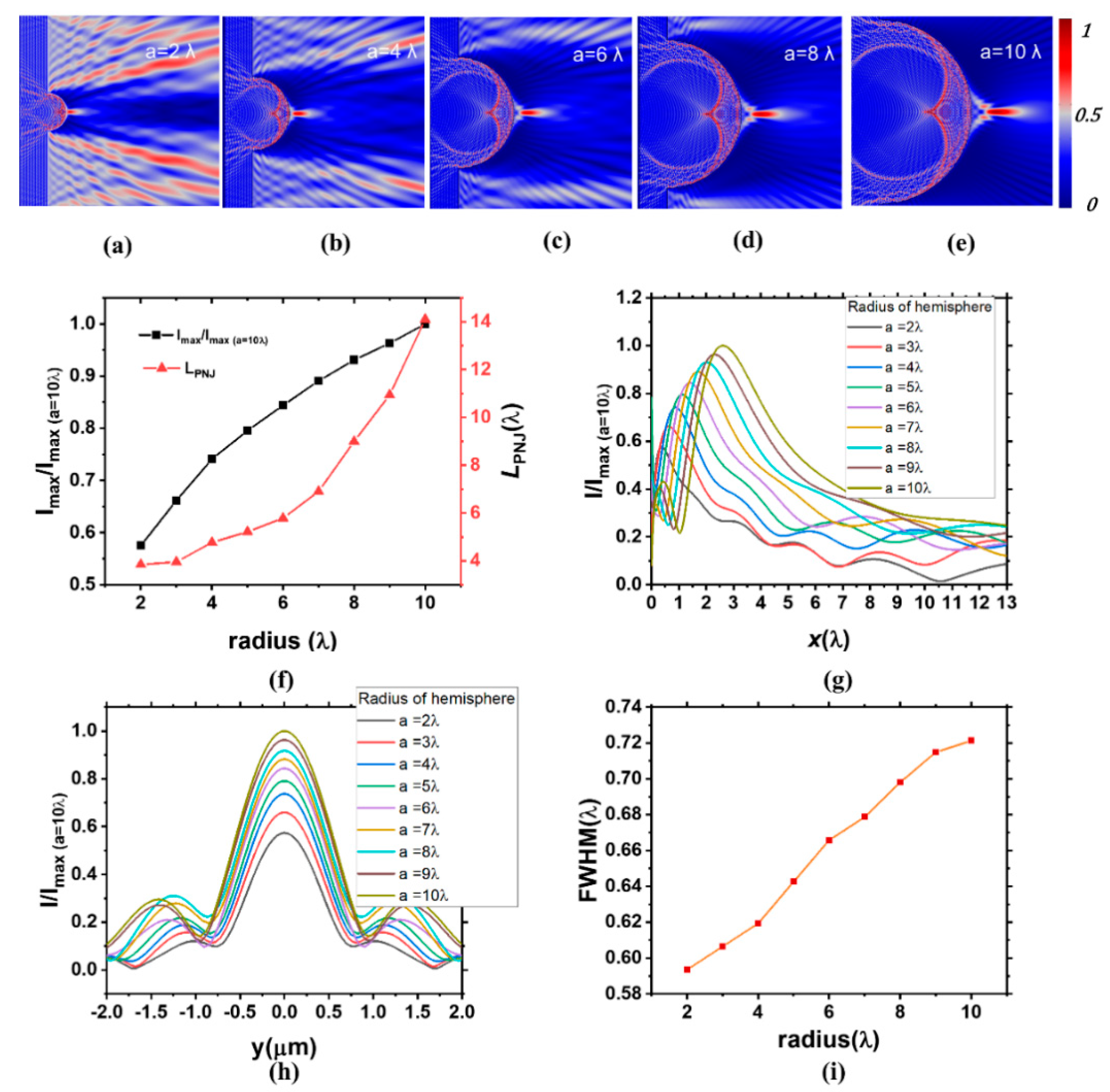
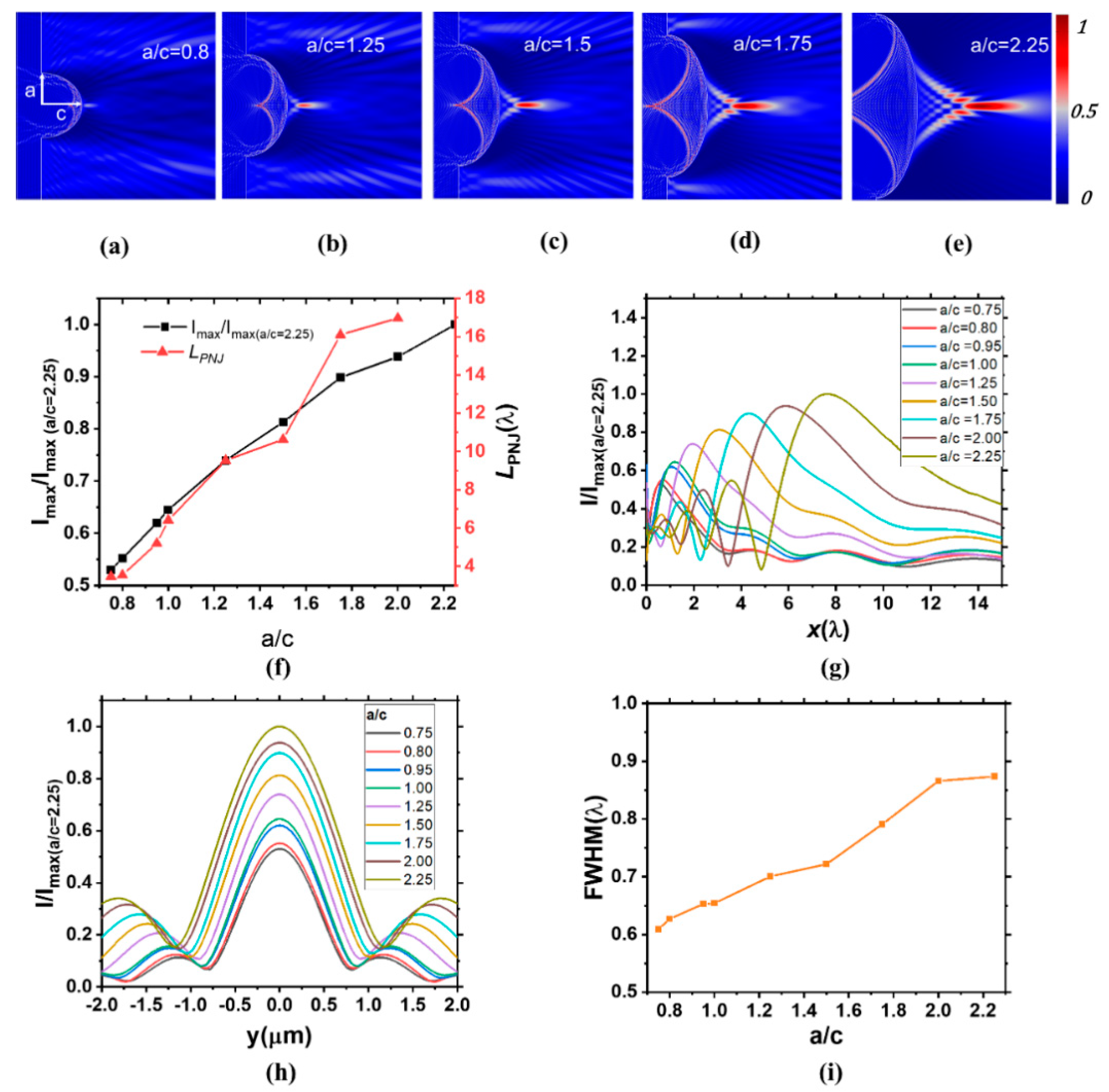
4. Effect of Radius of Dome

The behaviour of PNJ as a function of radius of hemisphere was studied. Figure 3a–e shows the PNJ generated from hemispheres of radius varying from 2 λ to 10 λ . As the radius of the hemisphere increased, the PNJ moved away from the refracting surface. Figure 3f shows the electric field intensity of the PNJ at its waist normalized to the electric field of the PNJ of the hemisphere of radius a = 10 λ . The maximum intensity ( I m a x ) of PNJ increased with increase in the size of the dome. The length of PNJ as a function of radius is also plotted in Figure 3f. Similar to the intensity, the length of the PNJ ( L P N J ) also increased with increase in the size of the dome. For a radius of 10 λ , the PNJ was longer than 14 λ (Figure 3f) As the radius increased, the field maxima occurred further away from the refracting surface (Figure 3g). The electric field intensity across the PNJ beam waist is plotted in Figure 3h. All curves are normalized to the I m a x produced by a = 10 λ . The FWHM of the PNJs as a function of the radius is shown Figure 3i. The beam waist gradually increased with increase in the radius of the hemispherical dome. We could also see the caustics formed by the reflection of the incident wave from the Si dome at the interior of the dome.

5. Effect of Sphericity of the Dome

It is intriguing to understand how the sphericity of the dome affects the PNJ. Lithography/etching techniques sometimes generate spheroids and therefore it is important to understand how PNJ behaves with change in sphericity of the hemisphere. To understand the effect, we simulated spheroids. In these simulations, the semi-axis to the pole (c) was kept as 5 λ and semi-axis in the equator (a) varied. All calculations were done at 1550 nm. The intensity of PNJs generated by the prolate spheroids was low compared to oblate spheroids and their lengths are very short. Figure 4a–e shows the PNJ formed from the spheroids with a / c ratio 0.8, 1.25, 1.5, 1.75, and 2.25, respectively. Both the length and intensity of the PNJ increased with increase in the a / c ratio. The I m a x of PNJs normalized to the I m a x of PNJ produced by the dome of a / c = 2.25 as a function of a/c ratio is shown in Figure 4f. The L P N J of different domes is also plotted in Figure 4f. The I m a x of PNJ as well as L P N J increased linearly with the increase in a/c ratio of the dome. An L P N J of 17 λ was observed when a/c was 2 which is 2.25 times longer compared to the hemispherical domes ( a / c = 1 ). The PNJ progressively moved away from the refracting surface with increase in a / c ratio (Figure 4g). For an a / c ratio of 2, the PNJ occurs about 6 λ away from the refracting surface. PNJ formation further away from the refracting surface of the hemispherical dome can be advantageous when the domes are used as imaging elements because it offers longer working distance. We also observed that the caustics at the interior of the particle moved away from the pole as the a / c was increased. The electric field intensity across the waist of the PNJ as a function of a / c ratio is shown in Figure 4h. All curves are normalized to the electric field intensity maximum of the curve with a / c = 2.25 . The beam waist of PNJ increased with increase in the a/c ratio and the FWHMs of the PNJs with various a/c ratio are shown in Figure 4i. This observation is different from that observed in oblate spheroids, where the beam width decreased with increase in a / c [25].

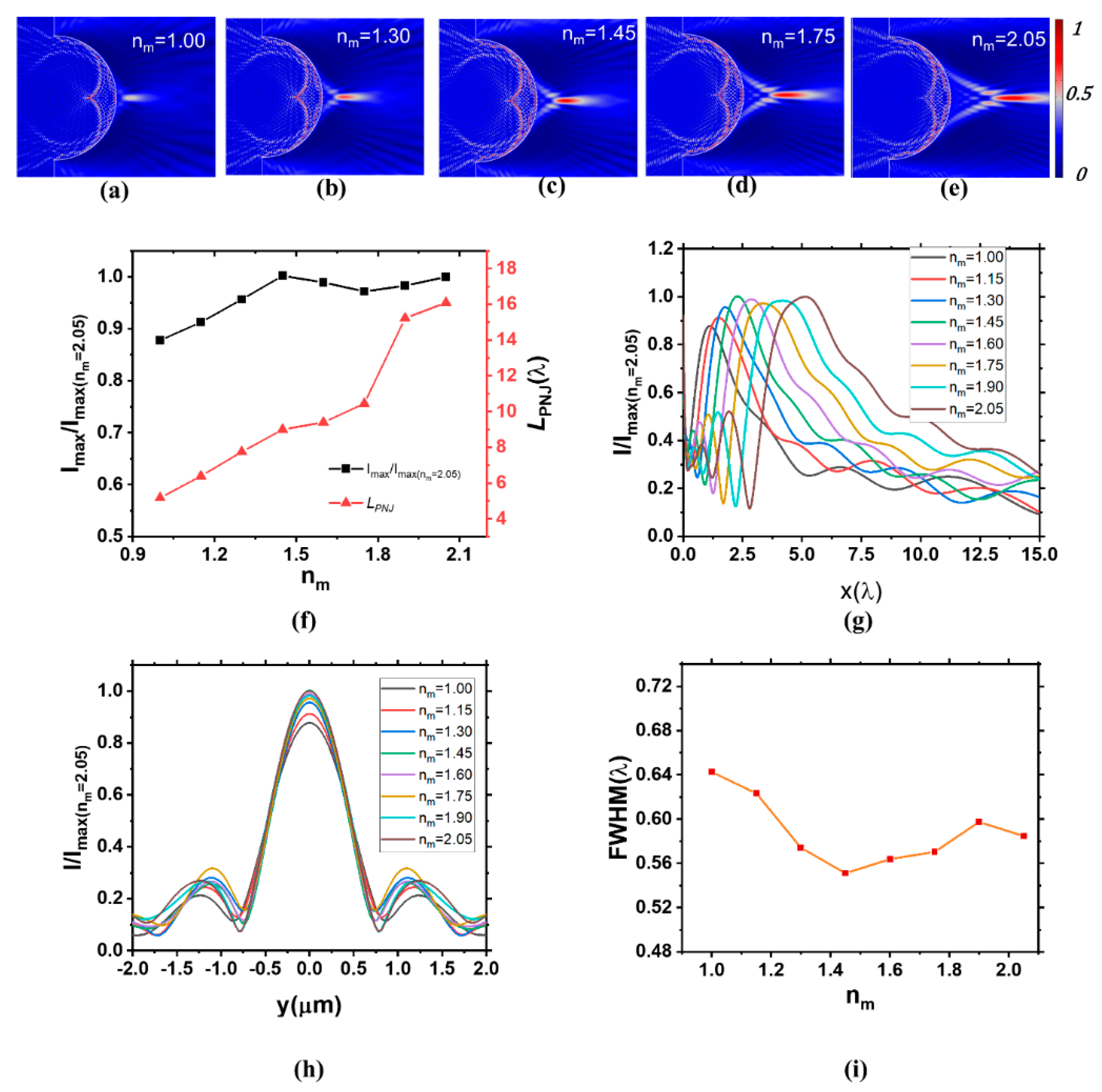
6. Significance of the Substrate and Medium Refractive Indices

Properties of the PNJs are affected by the refractive indices of the particle as well as the surrounding medium. To understand how the refractive index of the surrounding medium ( n m ) affect the properties of PNJ of hemispherical domes, we simulated the structures by varying the surrounding refractive index from 1 to 2.05. The range 1.3 to 1.8 can be easily covered from commercially available index matching liquids [26]. A refractive index above 1.8 was included in the study to get a better understanding of the effect of surrounding medium at a much higher refractive index. Figure 5a–e shows the PNJs as a function of the surrounding refractive index. With increase in n m , the PNJ moved away from the hemispherical dome and became longer. This shows that the length of PNJ of the hemi-spherical dome was inversely proportional to the refractive index contrast of the dome and surrounding medium. Figure 5f shows the I m a x of PNJs normalized to the I m a x of PNJ of n m = 2.05 . The PNJ intensity increased until the n m reached a value of 1.45 and then stayed relatively stable. The length of PNJ as a function surrounding refractive index is also shown in Figure 5f. The L P N J gradually increased with increase in n m . At refractive index n m 1.74 , a drastic increase in LPNJ could be seen. This happened because at those indices, the effective refractive index of the dome was approaching the small index contrast limit ( n e f f < 2 ) [19,21]. The electric field intensity normalized to I m a x   o f   n m = 2.05 , along the length of PNJ is shown in Figure 5g. With increase in   n m , the PNJ moved further away from the hemispherical dome. The normalized electric field across the beam waist of the PNJ is shown in Figure 5h. The FWHM of the PNJ gradually decreased until the n m reached a value of 1.45 (Figure 5i). Further increase in the n m slightly broadened the PNJ.

7. Conclusions

In conclusion, we proposed a structure consisting of a hemispherical dome of Si on a Si substrate that oversteps the refractive index limit of 2 to generate PNJ outside the structure. The proposed design is CMOS-compatible and can be easily fabricated using standard microfabrication techniques. We studied the nanojet confinement using a FEM model and the results show that the designed structure supports PNJ. The length and beam waist of PNJ can be varied by changing the radius of the dome. The length and beam waist of the PNJ increase gradually with increase in the radius of the dome. The width and length of the PNJ can also be controlled by controlling the sphericity of the dome. Oblate spheroids generate longer PNJs and the waist of PNJ is further away from the refracting surface. Such PNJ can offer longer working distance if used in imaging. The surrounding refractive index also affect the PNJ of hemispherical domes. The PNJ length and intensity increase with increase in surrounding refractive index. The width of PNJ decreases with increase in surrounding refractive index up to 1.45 and further increase broadens the PNJ. To the best of our knowledge, what we proposed is the first ever design that supports PNJ outside the structure for a material with refractive index contrast of more than 2 and on a Si chip that can exploit simple and standard microfabrication. These chips can be integrated into microfluidic devices for applications such as spectroscopy, particle tracking, and optical trapping. It is also possible to produce an array of these domes to use as a focal point array for super resolution imaging.

Author Contributions

A.V.V. conceived the idea together with G.S.M. A.V.V. performed the design and simulation of the on-chip PNJ. G.S.M. supervised the work and provided funding. A.V.V. mainly wrote the paper with significant input from G.S.M. All authors have read and agreed to the published version of the manuscript.

Funding

This work was supported by the UK Engineering and Physical Sciences Research Council (EPSRC grant EP/S03109X/1).

Institutional Review Board Statement

Not applicable.

Informed Consent Statement

Not applicable, the study does not involve humans.

Data Availability Statement

The data for this work are accessible through the University of Southampton Institutional Research Repository (https://doi.org/10.5258/SOTON/D2046).

Acknowledgments

The authors acknowledge the use of the IRIDIS High Performance Computing Facility, and associated support services at the University of Southampton.

Conflicts of Interest

The authors declare no conflict of interest.

References

  1. Chen, Z.; Taflove, A.; Backman, V. Photonic nanojet enhancement of backscattering of light by nanoparticles: A potential novel visible-light ultramicroscopy technique. Opt. Express 2004, 12, 1214. [Google Scholar] [CrossRef]
  2. Heifetz, A.; Kong, S.-C.; Sahakian, A.V.; Taflove, A.; Backman, V. Photonic nanojets. J. Comput. Theor. Nanosci. 2009, 6, 1979–1992. [Google Scholar] [CrossRef]
  3. Dantham, V.R.; Bisht, P.B.; Namboodiri, C.K.R. Enhancement of Raman scattering by two orders of magnitude using photonic nanojet of a microsphere. J. Appl. Phys. 2011, 109, 103103. [Google Scholar] [CrossRef]
  4. Veluthandath, A.V.; Bisht, P.B. Identification of Whispering Gallery Mode (WGM) coupled photoluminescence and Raman modes in complex spectra of MoS2 in Polymethyl methacrylate (PMMA) microspheres. J. Lumin. 2017, 187, 255–259. [Google Scholar] [CrossRef]
  5. Li, X.; Chen, Z.; Taflove, A.; Backman, V. Optical analysis of nanoparticles via enhanced backscattering facilitated by 3-D photonic nanojets. Opt. Express 2005, 13, 526. [Google Scholar] [CrossRef] [Green Version]
  6. Lecler, S.; Haacke, S.; Lecong, N.; Crégut, O.; Rehspringer, J.-L.; Hirlimann, C. Photonic jet driven non-linear optics: Example of two-photon fluorescence enhancement by dielectric microspheres. Opt. Express 2007, 15, 4935. [Google Scholar] [CrossRef]
  7. Born, B.; Geoffroy-Gagnon, S.; Krupa, J.D.A.; Hristovski, I.R.; Collier, C.M.; Holzman, J.F. Ultrafast All-Optical Switching via Subdiffractional Photonic Nanojets and Select Semiconductor Nanoparticles. ACS Photonics 2016, 3, 1095–1101. [Google Scholar] [CrossRef] [Green Version]
  8. Yang, H.; Trouillon, R.; Huszka, G.; Gijs, M.A.M. Super-resolution imaging of a dielectric microsphere is governed by the waist of its photonic nanojet. Nano Lett. 2016, 16, 4862–4870. [Google Scholar] [CrossRef]
  9. Du, B.; Zhang, H.; Xia, J.; Wu, J.; Ding, H.; Tong, G. Super-Resolution Imaging with Direct Laser Writing-Printed Microstructures. J. Phys. Chem. A 2020, 124, 7211–7216. [Google Scholar] [CrossRef]
  10. Darafsheh, A. Photonic nanojets and their applications. J. Phys. Photonics 2021, 3, 21. [Google Scholar] [CrossRef]
  11. Kim, J.; Cho, K.; Kim, I.; Kim, W.M.; Lee, T.S.; Lee, K.S. Fabrication of plasmonic nanodiscs by photonic nanojet lithography. Appl. Phys. Express 2012, 5, 3. [Google Scholar] [CrossRef]
  12. Jacassi, A.; Tantussi, F.; Dipalo, M.; Biagini, C.; MacCaferri, N.; Bozzola, A.; De Angelis, F. Scanning Probe Photonic Nanojet Lithography. ACS Appl. Mater. Interfaces 2017, 9, 32386–32393. [Google Scholar] [CrossRef] [Green Version]
  13. Wu, W.; Katsnelson, A.; Memis, O.G.; Mohseni, H. A deep sub-wavelength process for the formation of highly uniform arrays of nanoholes and nanopillars. Nanotechnology 2007, 18. [Google Scholar] [CrossRef]
  14. Yang, H.; Cornaglia, M.; Gijs, M.A.M. Photonic nanojet array for fast detection of single nanoparticles in a flow. Nano Lett. 2015, 15, 1730–1735. [Google Scholar] [CrossRef] [PubMed]
  15. Neves, A.A.R. Photonic nanojets in optical tweezers. J. Quant. Spectrosc. Radiat. Transf. 2015, 162, 122–132. [Google Scholar] [CrossRef] [Green Version]
  16. Li, Y.; Xin, H.; Liu, X.; Zhang, Y.; Lei, H.; Li, B. Trapping and Detection of Nanoparticles and Cells Using a Parallel Photonic Nanojet Array. ACS Nano 2016, 10, 5800–5808. [Google Scholar] [CrossRef] [PubMed]
  17. Gu, G.; Song, J.; Liang, H.; Zhao, M.; Chen, Y.; Qu, J. Overstepping the upper refractive index limit to form ultra-narrow photonic nanojets. Sci. Rep. 2017, 7, 5635. [Google Scholar] [CrossRef]
  18. Luk’yanchuk, B.S.; Paniagua-Domínguez, R.; Minin, I.; Minin, O.; Wang, Z. Refractive index less than two: Photonic nanojets yesterday, today and tomorrow [Invited]. Opt. Mater. Express 2017, 7, 1820. [Google Scholar] [CrossRef]
  19. Pacheco-Peña, V.; Beruete, M. Photonic nanojets with mesoscale high-index dielectric particles. J. Appl. Phys. 2019, 125. [Google Scholar] [CrossRef]
  20. Zhen, Z.; Huang, Y.; Feng, Y.; Shen, Y.; Li, Z. An ultranarrow photonic nanojet formed by an engineered two-layer microcylinder of high refractive-index materials. Opt. Express 2019, 27, 9178. [Google Scholar] [CrossRef]
  21. Geints, Y.E.; Zemlyanov, A.A.; Minin, I.V.; Minin, O.V. Overcoming refractive index limit of mesoscale light focusing by means of specular-reflection photonic nanojet. Opt. Lett. 2020, 45, 3885–3888. [Google Scholar] [CrossRef] [PubMed]
  22. Zhou, S.; Zhou, T. An ultra-narrow photonic nanojet generated from a high refractive-index micro-flat-ended cylinder. Appl. Phys. Express 2020, 13, 42010. [Google Scholar] [CrossRef]
  23. Loomis, J.; Ratnayake, D.; McKenna, C.; Walsh, K.M. Grayscale lithography—Automated mask generation for complex three-dimensional topography. J. Micro/Nanolithogr. MEMS MOEMS 2016, 15, 013511. [Google Scholar] [CrossRef]
  24. Lee, G.J.; Kim, H.M.; Song, Y.M. Design and fabrication of microscale, thin-film silicon solid immersion lenses for mid-infrared application. Micromachines 2020, 11, 250. [Google Scholar] [CrossRef] [PubMed] [Green Version]
  25. Jalali, T.; Erni, D. Highly confined photonic nanojet from elliptical particles. J. Mod. Opt. 2014, 61, 1069–1076. [Google Scholar] [CrossRef]
  26. Cargille Refractive Index Liquids. Available online: https://www.cargille.com/available-refractive-indices-sds-datasheets/ (accessed on 9 December 2021).
Figure 1. Normalized electric field intensity profile of PNJ in a silica microsphere ( n = 1.44 ) of radius 5 λ in vacuum (a) and PNJ of Si microsphere of same radius (b). Inset shows the close-up of PNJ in Si microsphere.
Photonics 08 00586 g001
Figure 2. The geometry of the proposed structure (a). Electric field intensity patterns of PNJ formed in a photonic chip with Si−hemisphere (b). A prominent PNJ can be seen at the exterior of hemisphere. Transverse intensity profile is shown in (c) and the length in (d).
Photonics 08 00586 g002
Figure 3. PNJ generated by hemispherical domes of different radii (ae). The maximum intensity ( I m a x ) normalized to I m a x   of dome of a = 10 λ and the L P N J as a function of radius are shown in (f). Normalized electric field intensity along the length of PNJ is shown in (g). Normalized electric field intensity across the beam waist and FWHM as a function of radius are shown in (h) and (i), respectively.
Photonics 08 00586 g003
Figure 4. Electric field intensity of PNJ with varying equatorial radius of the dome (ae). Maximum electric field intensity ( I m a x ) normalized to I m a x of a / c = 2.25 and L P N J are shown in (f). Normalized electric field intensity along the length of PNJ from the pole of the dome is shown in (g). All curves are normalized to the I m a x of a / c = 2.25 . Relative field intensity across the PNJ waist is shown in (h). The FWHM of PNJ beam waist as function of ratio of equatorial and polar radius is shown in (i).
Photonics 08 00586 g004
Figure 5. Intensity of electric field of PNJ with n m = 1, 1.3, 1.45, 1.75, and 2.05 (ae). Maximum electric field intensity ( I m a x ) normalized to I m a x   ( n m = 2.05 ) and L P N J (f). Electric field intensity relative to I m a x of n m = 2.05 along the length of PNJ (g). I / I m a x ( n m = 2.05 ) across the PNJ waist is shown in (h). FWHM of the PNJs as a function of surrounding refractive index is shown in (i).
Photonics 08 00586 g005
Publisher’s Note: MDPI stays neutral with regard to jurisdictional claims in published maps and institutional affiliations.

