Article

Microstrip Array Ring FETs with 2D p-Ga2O3 Channels Grown by MOCVD

by
Manijeh Razeghi
1,*,
Junhee Lee
1,
Lakshay Gautam
1,
Jean-Pierre Leburton
2,
Ferechteh H. Teherani
3,
Pedram Khalili Amiri
4,
Vinayak P. Dravid
5,6 and
Dimitris Pavlidis
7
1
Center for Quantum Devices, Department of Electrical Engineering and Computer Science, Northwestern University, Evanston, IL 60208, USA
2
Department of Electrical and Computer Engineering, University of Illinois Urbana-Champaign, Champaign, IL 61801, USA
3
Nanovation, 78117 Chateaufort, France
4
Department of Electrical and Computer Engineering, Northwestern University, Evanston, IL 60208, USA
5
Department of Materials Science and Engineering, Northwestern University, Evanston, IL 60208, USA
6
NUANCE Center, Northwestern University, Evanston, IL 60208, USA
7
College of Engineering and Computing, Florida International University, Miami, FL 33174, USA
*
Author to whom correspondence should be addressed.
Photonics 2021, 8(12), 578; https://doi.org/10.3390/photonics8120578
Submission received: 3 November 2021 / Revised: 3 December 2021 / Accepted: 12 December 2021 / Published: 14 December 2021

Abstract

:
Gallium oxide (Ga2O3) thin films of various thicknesses were grown on sapphire (0001) substrates by metal organic chemical vapor deposition (MOCVD) using trimethylgallium (TMGa), high purity deionized water, and silane (SiH4) as gallium, oxygen, and silicon precursors, respectively. N2 was used as carrier gas. Hall measurements revealed that films grown with a lower VI/III ratio had a dominant p-type conduction with room temperature mobilities up to 7 cm2/Vs and carrier concentrations up to ~1020 cm−3 for thinner layers. High resolution transmission electron microscopy suggested that the layers were mainly κ phase. Microstrip field-effect transistors (FETs) were fabricated using 2D p-type Ga2O3:Si, channels. They achieved a maximum drain current of 2.19 mA and an on/off ratio as high as ~108. A phenomenological model for the p-type conduction was also presented. As the first demonstration of a p-type Ga2O3, this work represents a significant advance which is state of the art, which would allow the fabrication of p-n junction based devices which could be smaller/thinner and bring both cost (more devices/wafer and less growth time) and operating speed (due to miniaturization) advantages. Moreover, the first scaling down to 2D device channels opens the prospect of faster devices and improved heat evacuation.

1. Introduction

Recently, gallium oxide (Ga2O3) with an ultra-wide bandgap (UWBG) of ~4.9 eV has emerged as a next generation semiconductor material for high power electronic devices. This is in great part due to its high breakdown electric field (~8 MV/cm), which largely surpasses that of competing materials systems such as SiC or GaN. Furthermore, the emergence of n-type doping capacity and single crystal Ga2O3 substrates has allowed the development of various unipolar electronic devices including metal oxide semiconductor field effect transistors (MOSFETs), Schottky diodes, and metal semiconductor field effect transistors (MESFET), which have been demonstrated based on high quality homo-epitaxial growth [1,2,3]. The vast majority of this work has focused on homoepitaxial growth of monoclinic β-Ga2O3, which is the most stable of five common polytypes α-, β-, γ-, ε-, and κ). A major drawback of β-Ga2O3 until recently, however, has been lack of a method to obtain p-type conduction; this is a key limitation for its adoption in a whole range of semiconductor device applications. Moreover, the relatively low thermal conductivity of Ga2O3 and the problem of Ga2O3 substrate cost being two orders of magnitude higher than sapphire are both currently hindering the fuller development of Ga2O3-based powered electronics. In previous studies, we showed that κ-Ga2O3 (an orthorhombic polymorph which is normally considered to be transient) could be stabilized in heteroepitaxial growth on sapphire (0001) substrates by MOCVD [4,5,6,7,8,9,10,11,12]. In this work, we found that high levels of shallow acceptor p-type conduction could be achieved in such layers using silicon impurity doping under Ga rich growth conditions. We then processed 2D layers of such p-type Ga2O3:Si into microstrip array ring FETs using conventional photolithography. The operational characteristics of the FETs proved to be consistent with p-type conduction. This is the first demonstration of both shallow acceptors doping of Ga2O3 and a p-type Ga2O3 channel FET. A phenomenological model that is coherent with a p-type channel is also presented.

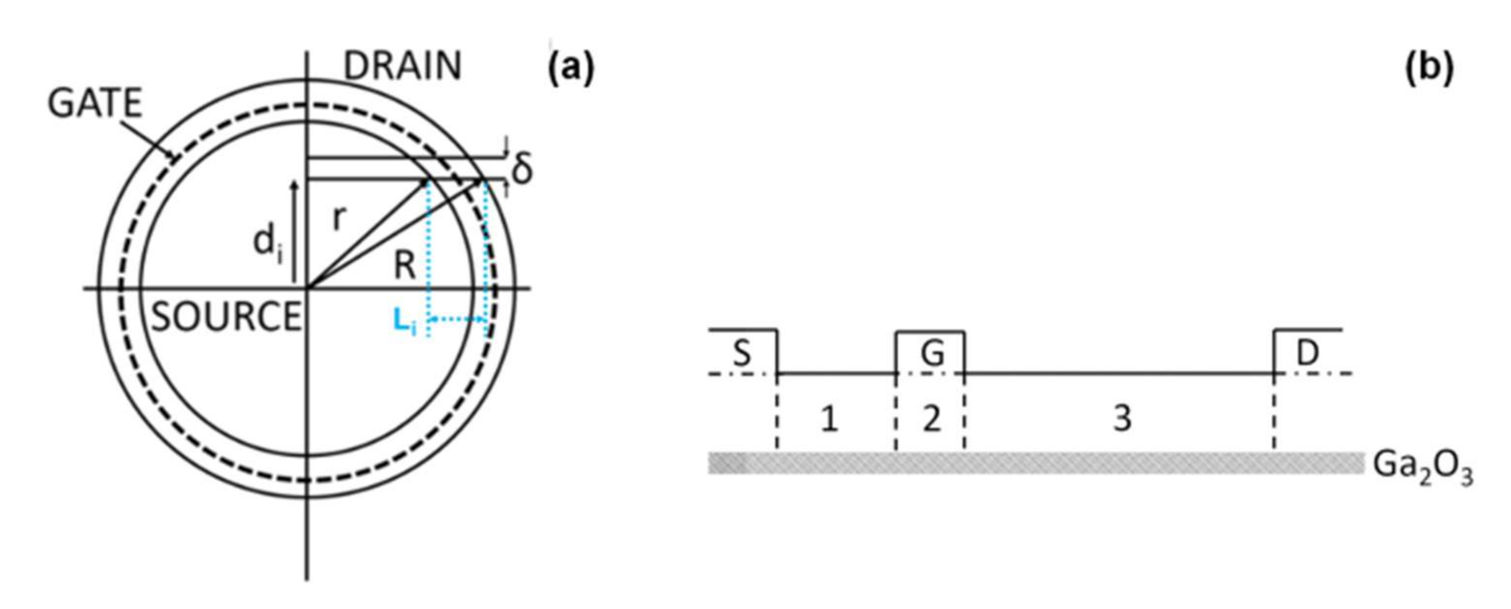
2. Materials and Methods
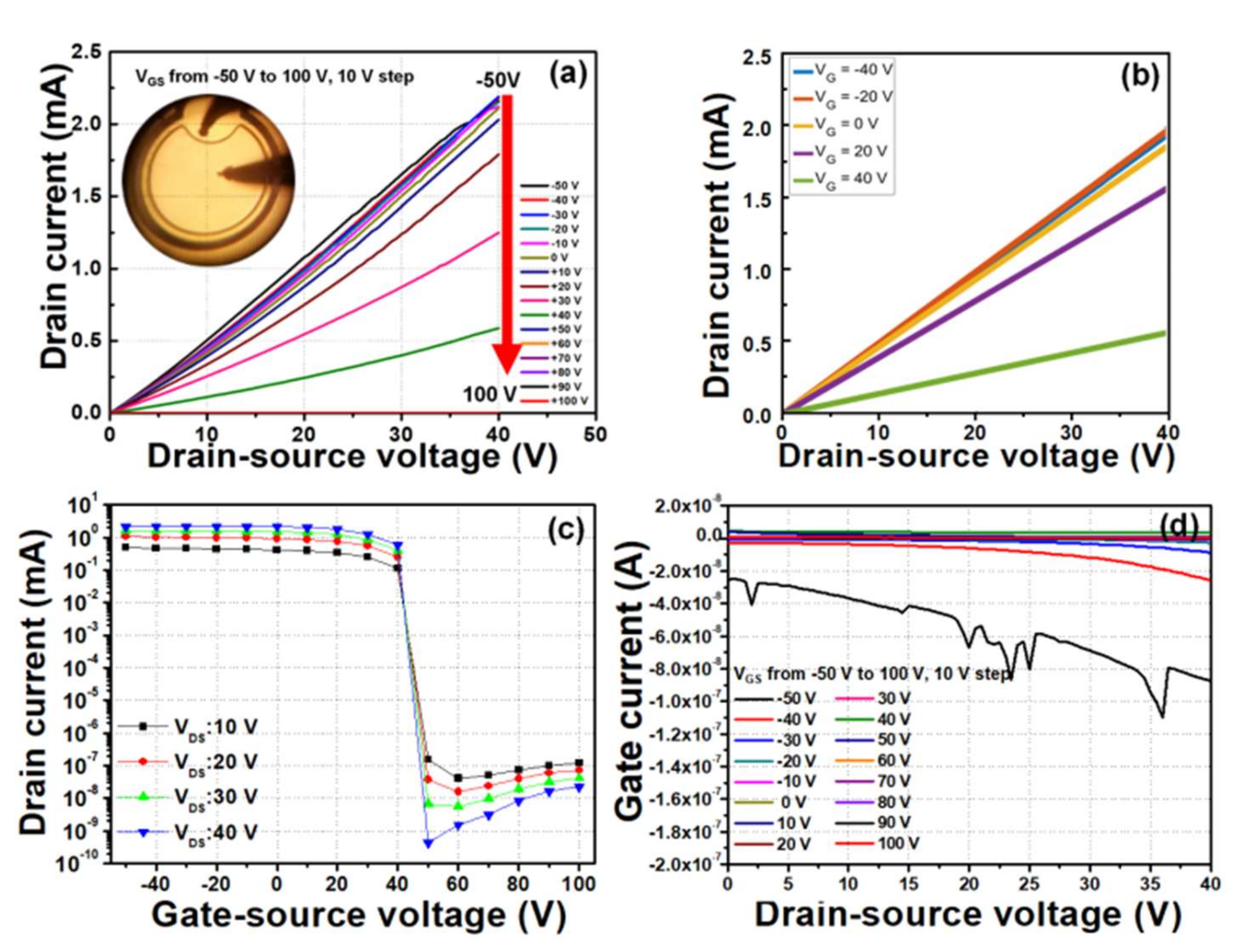
A commercial MOCVD reactor (AIXTRON 200/4 RF) was used to grow Ga2O3 on sapphire (0001) substrates at growth temperatures ranging from 730 °C to 1000 °C. Trimethylgallium (TMGa), high purity deionized water and SiH4 were adopted as the Ga, O and Si precursors, respectively. N2 was used as the carrier gas. The total pressure was 50 mbar. The VI/III ratio was either 100 (Ga-rich) or 150 (O-rich). The SiH4 flow rate was fixed at 15 sccm [4,5,6,7,8,9,10,11,12].

3. Results

XRD analysis was performed (Figure 1) to analyze the phases of the grown ~150 nm thick Ga2O3:Si with different VI/III ratio 100 and 150. The XRD results showed three peaks for each Ga2O3:Si layer. The three peaks that were observed were similar to the results of the β-Ga2O3 substrate (Figure 1). However, the TEM analysis in Figure 1d showed the result of κ-phase with the space group of Pna21 [4,5,10]. This metastable and transient κ-Ga2O3 was also identified by Playford et al. [13]. The κ-phase Ga2O3:Si was grown in the (002) direction and the six rotated domains were observed in the ~150 nm thick Ga2O3:Si.
Electrical properties were measured using Van der Pauw Hall measurements. Ohmic contacts were obtained using a Ga/In eutectic. Figure 2a,b show the results as a function of growth temperature for both VI/III ratios. At a VI/III ratio of 150, Ga2O3:Si that was grown at 730 °C shows n-type characteristics and the carrier concentration is ~2.6 × 1018 cm−3. The average resistivity is measured as ~4.3 Ω·cm. As the growth temperature was increased from 730 °C to 1000 °C, the carrier concentration decreased linearly to ~4.4 × 1017 cm−3. Such a tendency is reminiscent of the amphoteric doping of GaAs with Si [14,15]. In the case of GaAs, p-type Si doping behavior was obtained for a relatively low V/III ratio and growth temperature [16,17,18]. Assuming that the Si dopant acts as a shallow acceptor by substituting on the O-site of the Ga2O3, the VI/III ratio of 100 growth condition could be expected to a generate higher density of oxygen vacancies (VO) by virtue of the Ga-rich nature of the growth which lets the Si substitute more readily at the O-sites. This assumption is coherent with Figure 2c which shows the Hall mobility of the Ga2O3:Si as a function of growth temperature for VI/III ratios of 150 and 100. For a VI/III ratio of 150, an n-type mobility near 50 cm2/Vs was observed for a growth temperature of 1000 °C. For a VI/III ratio of 100, a p-type mobility of ~3.3 cm2/Vs was observed. This demonstrates Si being an amphoteric dopant in κ-Ga2O3. Si impurity doping is generally incorporated to substitute for Ga where it acts as a shallow donor to create heavily doped n-type Ga2O3. But as the density of VO increases under Ga-rich growth conditions, the above results suggest that Si can act as a shallow acceptor by substituting on the O-sites in κ-Ga2O3, and thus promote a transformation to predominantly p-type conduction. These p-type results were confirmed via theoretical and experimental measurements by multiple groups [19,20,21].
Ring type FETs were fabricated and evaluated for the characteristics of the FET device of ~150 nm thick p-type Ga2O3:Si with VI/III ratio of 100. Figure 3 shows the I-V curves; a negative bias voltage was applied to the drain terminal and the Vds values of all presented experimental and theoretical results correspond to the magnitude of drain-source voltage |Vds|. It was observed that the drain current decreased with increasing gate voltage. However, it was not possible to achieve pinch-off due to the gate electrode burning at gate voltages higher than 50 V. To avoid this issue, the channel thickness was reduced to ~1.2 nm and the ring pattern FETs were patterned with microstrips. Ga2O3:Si channel layers were grown at 1000 °C with a VI/III ratio of 100. The channel thickness was estimated to be ~1.2 ± 0.5 nm based on the interferometric growth rate calibration and AFM step-edge profilometry. Hall measurements confirmed the p-type nature of the layers with a resistivity of ~0.007 Ω ·cm, a carrier concentration of ~1.7 × 1020 cm−3, and a mobility of ~5.7 cm2/Vs.
Standard photolithography and lift-off were employed to deposit source and drain metal contacts. Before their deposition, 3 μm × 3 μm microstrip patterns were formed by electron cyclotron resonance-reactive ion etching (ECR-RIE) with CF4 for 5 min. The metal contacts were Ti (20 nm)/Au (150 nm) deposited by e-beam evaporation. SiO2 of 100 nm thick gate dielectric material was formed by plasma-enhanced chemical vapor deposition (PECVD). After dielectric and passivation film deposition, the gate metal contact was formed with Pt (20 nm)/Ti (20 nm)/Au (150 nm) on the SiO2 film. The gate length, and the spacing between the source/drain and the inside source circular pad were 15, 20, and 100 μm, respectively. Figure 4a shows schematic illustrations of the device with top- and cross-sectional views illustrating the device scale. Figure 4b shows an optical microscope image of the fabricated devices.
The FETs were then fabricated and tested using a semiconductor parameter analyzer and probe station. Figure 5a shows the DC source-drain current versus source-drain voltage (IDS–VDS) output characteristics for the depletion-mode FETs that were measured by increasing the gate-source voltage (VGS) stepwise from −50 to 100 V. The maximum IDS was 2.19 mA and it was effectively modulated by VGS from −50 to 100 V, which is coherent with a p-type channel. Because of the heavy p-doping, the 2D microstrip channel is normally-on, and the channel off-state was observed for a gate bias of 50 V (IDS = 0.1 pA at VDS of 40 V). In addition, because of the high sheet resistance, even with a drain voltage as high as 40 V, the voltage drop in the FET channel was still lower than |VG-VT|, which was the condition for current saturation in long channel FETs. As such, the IDS-VDS characteristics remained linear. Figure 5b displays a similar set of curves that were obtained from the simulation. It can be seen that the theoretical model is consistent with the experimental data in showing an output resistance increase with positive gate voltage and IDS bunching with little variation of the output resistance for VGS < 0. This is also consistent with a p-type channel. Figure 5c shows the transfer characteristics at VDS of 10 to 40 V in a logarithmic scale. The device achieved an on/off ratio of ~108 by minimizing the thickness and width of the channel. Figure 5d shows that IG increases above a VGS of 50 V because of a gate leakage current. It is expected that the on/off ratio can be further improved through the optimization of the dielectric layer.
A phenomenological model was developed that was based on the device configuration that is displayed in Figure 4. Figure 6 shows the schematic of the model device that consists of a linear array of δ = 3 μ m wide micro-strips that were separated from each other by δ = 3 μ m. They are covered by a disk-shaped source contact of 200 μm in diameter and separated from a square shaped drain by a 30 μ m wide circular channel. As such, in each quadrant, the channel length, Li, varies between a minimum value when it is perpendicular to the disk and a maximum value when it is tangential to the disk. The position of the ith microstrip is identified by its distance, di, from the center of the source disk.
At VG = 0 V, the channel is uniform and the current between source and drain in the ith micro-strip channel is given by
I i = e p s δ v i  
where e is the electron charge (C), p s is the 2D hole concentration (carriers/cm2), δ the wire width (cm), and v i is the hole velocity in the ith channel (cm/s). In the absence of saturation velocity (long channel-low mobility),
v i = μ V D S L i
where μ is the hole mobility (cm2/Vs) and L i is the channel length (cm).
If d i =   2 i δ   w i t h   0 i N , Equation (1) becomes for top and bottom right quadrants
I r i g h t =   2 i = 0 N I i = e p S μ V D S i = 0 N 1 / N + 5 2   i 2   N 2   i 2 = 2.84 e p S μ V D S  
Due to the relatively big gate pad on the left side of the source, the channel lengths are longer for a sizeable portion of the FIN-microstrips, so we estimate the total current should be multiplied by a factor η ~ 1.8–1.9 < 2. Finally,
I =   I R i g h t + I L e f t =   η I R i g h t
At V G 0 , the channel is made of three portions with different conductances (Figure 6b). By neglecting the contact resistance, we get for each channel,
I i V G = V D S 1 G 1 i + 1 G 2 i + 1 G 3 i   w i t h   G 1 , 3 i = e p s V G = 0 δ μ L 1 , 3 i     G 2 i = e p s V G 0 δ μ L 2 i
If P s V G 0   =   P s V G = 0 e x p e V c K T ,   where   V c V G   s the channel potential that is induced by the gate bias, the expression for the current reads
I i V G =   e p s V G = 0 δ μ V D S / L 1 i + L 2 i e x p e V C / k T + L 3 i
or after summation over all channels,
V G = 2 I V G = 0 1 + e x p e V C k T
This equation shows that for VC < 0 (VG< 0) the drain current decreases, whereas for VC > 0 (VG > 0) the drain current increases in agreement with the experimental data. This is coherent with the channel being a p-type. In quantitative terms, it shows that current decreases by several orders of magnitude under a positive VG compared to a limiting increase by a factor 2 under a negative VG. This asymmetry in the variation of the I-V characteristics for VG < 0 and VG> 0 is also consistent with the experimental data.
From the Poisson equation, one can derive an expression of VC for intermediate gate bias:
V C y = V G λ D e x p y D λ D D + λ D
where D is the thickness of the SiO2 barrier, y is the vertical coordinate inside the Ga2O3 layer, and λ D is the Debye length in the Ga2O3 layer that is fitted to reproduce the experimental I-V characteristics. Figure 5b displays the simulation data of I-V curves from VGS = −40 to 40 V, for which we used a channel mobility μ = 23 cm2/Vs and hole concentration ps = 2.35 × 10¹²/cm2.

4. Conclusions

In conclusion, κ -Ga2O3:Si layers that were grown on sapphire (0001) substrates by MOCVD showed consistent p-type Hall signal for layers that were grown with lower III/VI ratios during growth. The room temperature mobilities were up to 7 cm2/Vs, resistivities were as low as 0.007 Ω .cm, and the carrier concentrations were up to ~1020 cm−3 for thinner layers. The ring mesa FETs were fabricated based on ~1.2 nm thick p-Ga2O3:Si channels that were formed into a number of 3 μ m wide microstrips. The devices achieved a maximum drain current density of 2.19 mA and an on/off ratio of ~108 and showed characteristics that were consistent with a p-type conduction in the channel. The p-type Ga2O3 that was demonstrated in this work represents a significant advance and is state of the art, which may herald the fabrication of a range of p-n junction-based devices. These could be smaller/thinner and bring both cost (more devices/wafer and less growth time) and operating speed (due to miniaturization) advantages than current isotype FETs. Moreover, the demonstration of the first functioning devices based on scaling down to 2D device channels in Ga2O3 based FETs opens the prospect of faster devices and improved heat evacuation.

Author Contributions

Data curation, J.L., J.-P.L., F.H.T. and P.K.A.; Formal analysis, D.P.; Investigation, L.G. and V.P.D.; Project administration, M.R.; Writing—original draft, J.L. All authors have read and agreed to the published version of the manuscript.

Funding

This work is supported by USA Air Force under agreement of FA9550-19-1-0410.

Institutional Review Board Statement

Not applicable.

Informed Consent Statement

Not applicable.

Data Availability Statement

The data presented in this study are available on request from the corresponding author.

Acknowledgments

This work is supported by USA Air Force under agreement of FA9550-19-1-0410. The authors would like to acknowledge the support and interest of Ali Sayir of USAF-AFMC AFMCAFOSR/RTB).

Conflicts of Interest

The authors declare no conflict of interest.

References

  1. Higashiwaki, M.; Sasaki, K.; Kamimura, T.; Wong, M.H.; Krishnamurthy, D.; Kuramata, A.; Masui, T.; Yamakoshi, S. Depletion-mode Ga2O3 metal-oxide-semiconductor field-effect transistors on β-Ga2O3 (010) substrates and temperature dependence of their device characteristics. Appl. Phys. Lett. 2013, 103, 123511. [Google Scholar] [CrossRef] [Green Version]
  2. Sasaki, K.; Higashiwaki, M.; Kuramata, A.; Masui, T.; Yamakoshi, S.J. MBE grown Ga2O3 and its power device applications. Cryst. Growth 2013, 378, 591. [Google Scholar] [CrossRef]
  3. Sasaki, K.; Wakimoto, D.; Thieu, Q.T.; Koishikawa, Y.; Kuramata, A.; Higashiwaki, M.; Yamakoshi, S. First Demonstration of Ga2O3 Trench MOS-Type Schottky Barrier Diodes. IEEE Electron Device Lett. 2017, 38, 783. [Google Scholar] [CrossRef]
  4. Razeghi, M.; Park, J.-H.; McClintock, R.; Pavlidis, D.; Teherani, F.H.; Rogers, D.J.; Magill, B.A.; Khodaparast, G.A.; Xu, Y.; Wu, J.; et al. A review of the growth, doping, and applications of β-Ga2O3 thin films. In Proceedings of the SPIE, Oxide-Based Materials and Devices IX, San Francisco, CA, USA, 28 January–1 February 2018; Volume 10533, p. 105330R. [Google Scholar]
  5. Lee, J.; Kim, H.; Gautam, L.; He, K.; Hu, X.; Dravid, V.P.; Razeghi, M. Study of Phase Transition in MOCVD Grown Ga2O3 from κ to β Phase by Ex Situ and In Situ Annealing. Photonics 2021, 8, 17. [Google Scholar] [CrossRef]
  6. Lee, J.; Kim, H.; Gautam, L.; Razeghi, M. High Thermal Stability of κ-Ga2O3 Grown by MOCVD. Crystals 2021, 11, 446. [Google Scholar] [CrossRef]
  7. Lee, J.; Kim, H.; Gautam, L.; Razeghi, M. Highly Conductive Co-Doped Ga2O3:Si-In Grown by MOCVD. Coatings 2021, 11, 287. [Google Scholar] [CrossRef]
  8. Rogers, D.J.; Bove, P.; Arrateig, X.; Sandana, V.E.; Teherani, F.H.; Razeghi, M.; McClintock, R.; Frisch, E.; Harel, S. The new oxide paradigm for solid state ultraviolet photodetectors, Proceedings Volume 10533. In Proceedings of the SPIE 10533, Oxide-based Materials and Devices IX, 105331P, San Francisco, CA, USA, 30 April 2018. [Google Scholar]
  9. Park, J.-H.; McClintock, R.; Jaud, A.; Dehzangi, A.; Razeghi, M. MOCVD grown β-Ga2O3 metal-oxide-semiconductor field effect transistors on sapphire. Appl. Phys. Express 2019, 12, 095503. [Google Scholar] [CrossRef]
  10. Xu, Y.; Park, J.-H.; Yao, Z.; Wolverton, C.; Razeghi, M.; Wu, J.; Dravid, V.P. Strain-Induced Metastable Phase Stabilization in Ga2O3 Thin Films. ACS Appl. Mater. Interfaces 2019, 11, 5536–5543. [Google Scholar] [CrossRef] [PubMed]
  11. McClintock, R.; Jaud, A.; Gautam, L.; Razeghi, M. Solar-blind photodetectors based on Ga2O3 and III-nitrides. In Proceedings of the SPIE, Quantum Sensing and Nano Electronics and Photonics XVII, San Francisco, CA, USA, 24 March 2020; Volume 11288, p. 1128803. [Google Scholar]
  12. Park, J.-H.; McClintock, R.; Razeghi, M. Ga2O3 Metal-oxide-semiconductor Field Effect Transistors on Sapphire Substrate by MOCVD, Semicond. Sci. Technol. 2019, 34, 08LT01. [Google Scholar]
  13. Playford, H.Y.; Hannon, A.C.; Barney, E.R.; Walton, R.I. Structures of uncharacterised polymorphs of gallium oxide from total neutron diffraction. Chem. Eur. J. 2013, 19, 2803–2813. [Google Scholar] [CrossRef] [PubMed]
  14. Munoz-Yague, A.; Baceiredo, S.J. Ge Incorporation in GaAs Grown by Molecular Beam Epitaxy: A Thermodynamic Study. Electrochem. Soc. 1982, 129, 2108. [Google Scholar] [CrossRef]
  15. Teramoto, I.J. Calculation of distribution equilibrium of amphoteric silicon in gallium arsenide. Phys. Chem. Solids 1972, 33, 2089. [Google Scholar] [CrossRef]
  16. Meier, H.P.; Broom, R.F.; Epperlein, P.W.; van Giesen, E.; Harder, C.; Jäckel, H. Problems related to the formation of lateral p–n junctions on channeled substrate (100) GaAs for lasers. Vac. Sci. Technol. B 1988, 6, 692. [Google Scholar] [CrossRef]
  17. Agawa, K.; Hirakawa, K.; Sakamoto, N.; Hashimoto, Y.; Ikoma, T. Electrical properties of heavily Si-doped (311)A GaAs grown by molecular beam epitaxy. Appl. Phys. Lett. 1994, 65, 1171. [Google Scholar] [CrossRef]
  18. Quivy, A.A.; Sperandio, A.L.; Silva, E.C.F.; Leite, J.R. p-Type doping of GaAs (001) layers grown by MBE using silicon as a dopant. J. Cryst. Growth 1999, 206, 171. [Google Scholar] [CrossRef]
  19. Va, C.J.Z.I.; Kielara, S.M.; Jonesa, L.O.; Mosqueraa, M.A.; Schatz, G.C. Investigation of p-type doping in β-and κ-Ga2O3. J. Alloys Compd. 2021, 877, 160227. [Google Scholar]
  20. Lopez-Dominguez, V.; Shi, J.; Razeghi, M.; Amiri, P.K. “Magnetic Heterostructures using n- and p-doped Ga2O3 Films”, late news presentation. In Proceedings of the SPIE Quantum Sensing and Nano Electronics and Photonics XVI, San Francisco, CA, USA, 3–7 February 2019. [Google Scholar]
  21. Wang, C.; Park, J.-H.; Li, J.; McClintock, R.; Razeghi, M.; Grayson, M. “p-Type Ga2O3: P-type Hall, p-type Seebeck; mobility, anisotropy, and acceptor binding energy”, late news presentation. In Proceedings of the SPIE Quantum Sensing and Nano Electronics and Photonics XVI, San Francisco, CA, USA, 3–7 February 2019. [Google Scholar]
Figure 1. XRD omega/2theta scan of ~150 nm thick Ga2O3:Si with VI/III ratio (a) 150 and (b) 100; (c) XRD omega/2theta scan of β-Ga2O3 (TAMURA Corp); (d) TEM image of typical morphology of the ~150 nm thick Ga2O3:Si on sapphire, and an inset of the SAED patterns that were obtained along the (510) zone axis at the Ga2O3/Al2O3 interface. Ga2O3:Si with the space group Pna21 is identified.
Photonics 08 00578 g001
Figure 2. (a) Carrier concentration and resistivity of Ga2O3:Si on sapphire (0001) as a function of growth temperature at VI/III ratio 150; (b) carrier concentration and resistivity of Ga2O3:Si on sapphire (0001) as a function of growth temperature at VI/III ratio 100; (c) Hall mobility of Ga2O3:Si on sapphire (0001) as a function of growth temperature at VI/III ratio 100 and 150; (d) Table of ~150 nm thick hall measurement data measured in different groups.
Photonics 08 00578 g002
Figure 3. I-V curves of ~150 nm thick p-type Ga2O3:Si on sapphire (0001) from VGS = −10 V to 80 V and inset is an optical microscope image of the fabricated device.
Photonics 08 00578 g003
Figure 4. (a) Cross view and top view schematic illustration of 2D Ga2O3:Si channel microstrip array FETs with details of device scale; (b) Optical microscope image of the fabricated device.
Photonics 08 00578 g004
Figure 5. (a) I-V curves from VGS = −50 V to 100 V and the inset is an optical microscope image of the device during measurement using a probe station; (b) Simulation data of I-V curves from VGS = −40 V to 40 V; (c) transfer characteristics at VDS = 10 V to 40 V; (d) Gate current-drain source voltage characteristics with VGS increased stepwise from −50 V to 100 V.
Photonics 08 00578 g005
Figure 6. (a) Schematic illustration of the 2D Ga2O3:Si channel microstrip array FETs. (b) Schematic illustration of three portions of the Ga2O3 channel.
Photonics 08 00578 g006
Publisher’s Note: MDPI stays neutral with regard to jurisdictional claims in published maps and institutional affiliations.

