Article

Dual-Band, Polarization-Insensitive, Ultrathin and Flexible Metamaterial Absorber Based on High-Order Magnetic Resonance

1
Institute of Materials Science, Vietnam Academy of Science and Technology, 18 Hoang Quoc Viet, Cau Giay, Hanoi 100000, Vietnam
2
Graduate University of Science and Technology, Vietnam Academy of Science and Technology, 18 Hoang Quoc Viet, Hanoi 100000, Vietnam
3
Thai Nguyen University of Education, Thai Nguyen 250000, Vietnam
4
University of Transport and Communications, 3-Caugiay Str., Langthuong Award, Dongda Dist., Hanoi 100000, Vietnam
5
Department of Physics, Quantum Photonic Science Research Center and RINS, Hanyang University, Seoul 04763, Korea
6
Department of Optical Science and Engineering, Fudan University, Shanghai 200433, China
*
Author to whom correspondence should be addressed.
These authors have the same contribution.
Photonics 2021, 8(12), 574; https://doi.org/10.3390/photonics8120574
Submission received: 15 November 2021 / Revised: 5 December 2021 / Accepted: 10 December 2021 / Published: 14 December 2021

Abstract

:
We demonstrate a dual-band, polarization-insensitive, ultrathin and flexible metamaterial absorber (MA), based on high-order magnetic resonance. By exploiting a flexible polyimide substrate, the thickness of MA came to be 1/148 of the working wavelength. The absorption performance of the proposed structure was investigated for both planar and bending models. In the case of the planar model, a single peak was achieved at a frequency of 4.3 GHz, with an absorption of 98%. Furthermore, additional high-order absorption peaks were obtained by the bending structure on a cylindrical surface, while the fundamental peak with a high absorption was maintained well. Our work might be useful for the realization and the development of future devices, such as emitters, detectors, sensors, and energy converters.

1. Introduction

Metamaterial absorbers (MAs) have gained much attention because of their potential applications in sensing [1,2,3,4], imaging [5,6], and energy harvesting [7,8]. The first MA was introduced by Landy et al. in 2008, and consisted of two metallic elements on two sides of a dielectric layer [9]. Since then, MAs have become a hot topic and have been demonstrated in various frequency regions ranging from MHz [10,11] to optical frequencies [12,13]. Studies on MAs have been carried out in order to achieve the characteristic performances, such as high absorption [14], polarization-insensitive and wide-incidence-angle broadband [15,16,17,18], and multi-band [19]. Recently, flexibility has been one of the most important characteristics of MA [15,20,21,22,23].
MAs are generally constructed with a three-layer structure, in which a periodically-arranged metallic pattern is placed on a hard dielectric spacer, such as FR-4 [9,24] or vanadium oxide [18,25,26]. Although these MAs have a great absorption performance, they are limited in practical applications, especially in the case of rough surfaces because of their inflexibility. To overcome this disadvantage, flexible MAs have been proposed by using flexible substrates instead of hard ones, such as polyimide, polymer, or paper substrates [20,21,27].
Generally, multi-band absorption can be achieved by combining differently-shaped resonators in a unit cell, using a multilayer structure and the high-order resonance. For example, Yang et al. introduced a multi-band MA in which the electric ring resonator was rotated by 90° to form the symmetrical structure. In this model, the electromagnetic absorption at two frequencies was caused mainly by the electric resonance [28]. Zhao et al. demonstrated theoretically a twelve-band infrared MA by employing together the dipole, quadrupole, and octapole plasmon-resonance modes of four different ring-strip resonators [29]. Wang et al. designed and fabricated a triple-band THz MA with three concentric square-ring metallic resonators [30]. Recently, the methods to excite the high-order electric or magnetic resonances for the multi-band absorption in metamaterials have been reported by many researchers. Jung et al. showed that more than four absorption peaks were formed by only a single meta-atom, based on the odd-order magnetic and electric resonance [31]. Huang et al. investigated numerically an ultrathin triple-band MA working in the THz range, in which the high absorption peaks came from the high-order electromagnetic resonances (the electric quadrupolar, magnetic 2nd-harmonic, and magnetic 3rd-harmonic resonance) [32]. Khuyen et al. investigated the establishment of dual-band and high-order behavior in an ultrathin MA by controlling the oblique incidence of an electromagnetic wave in which the excited 3rd-harmonic resonance resulted in the appearance of high-order peaks [33]. Hien et al. proposed a triple-band MA, resulting from the third- and fifth-order magnetic resonances using ring-shaped structures [34]. In the discussion above, the high-order absorption was generated mainly by the excitation of odd-order magnetic resonances, while the even-order magnetic resonances are rare, owing to the dark-mode nature.
In this work, we present an ultrathin flexible multi-band MA, based on the fundamental and high-order oscillation model. In addition to the fundamental resonance, our results reveal that, when the proposed structure is bent on a cylindrical surface with a radius of 20 mm, the second-order resonance is excited. In the bending configuration, additional absorption peaks are developed while the fundamental one is maintained well with the near-unity absorption. Our obtained results contribute a way to create the second-order absorption mode in a simple metamaterial structure by bending the metamaterial absorber. This work might be useful to future work related to the exploitation of the even-order mode in MAs.

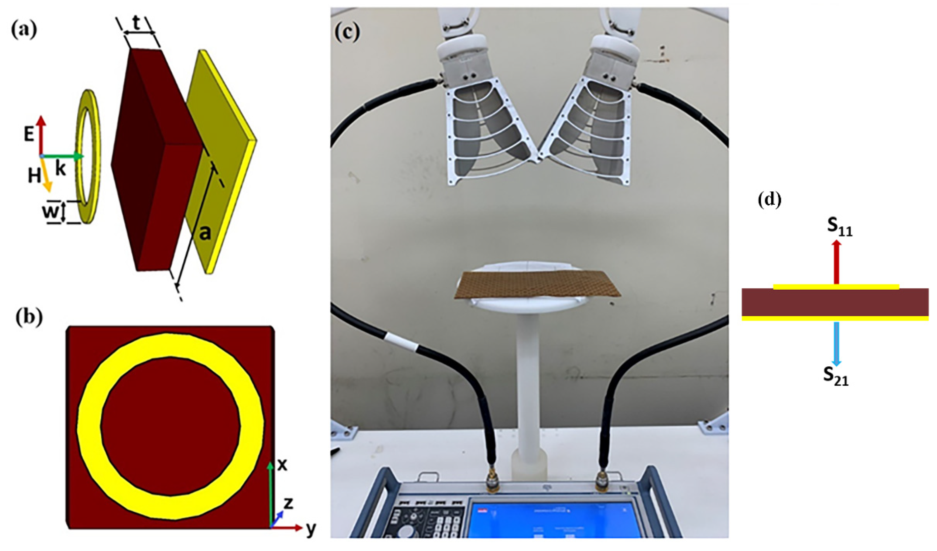
2. Metamaterial Structure and Methods

The structural model of a unit cell of the proposed MA is shown in Figure 1. This includes three layers which are a periodic ring-shaped structure on the top, a dielectric spacer at the middle, and a continuous metallic plane at the bottom. It is well-known that the properties of metamaterial are derived by the designed structure, rather than the chemical composition. Therefore, one can optimize the geometrical parameters in order to obtain the desired performance. Here, the geometrical parameters of the designed structure are the thickness of dielectric layer t, the width of ring w, and the size of unit cell a. Before optimizing these parameters, their values were set up to simulate the absorption behavior of the structure. For the case of polyimide substrate, a dielectric constant of 3.5 and a loss tangent of 0.0027 were employed. The top and bottom copper layers, with a thickness tm = 0.035 mm, were considered to have an electric conductivity of 5.96 × 10⁷ S/m. After the initial simulation, the geometrical parameters were optimized to be a = 16 mm, t = 0.4 mm, w = 1 mm, and the outer radius (R1) and inner radius (R2) of the ring were 7 and 6 mm, respectively.
Our simulation was performed by using the commercial Computer Simulation Technology (CST) Microwave Studio [35], in which the boundary conditions were set to be the unit cells for x- and y-directions and open for the z-direction. The absorption was calculated by A ( ω ) = 1 R ( ω ) T ( ω ) , where R ( ω ) = | S 11 | 2 and T ( ω ) = | S 21 | 2 are the reflection and transmission, respectively. Because the metallic film was located at the bottom of MA structure, the transmission was vanished, so the absorption came to be A ( ω ) = 1 R ( ω ) .
The proposed MA sample was fabricated with a polyimide board coated with copper, by the traditional lithography technique. A multilayer board of copper metal–polyimide dielectric–copper metal was used with a thickness of polyimide and copper of 0.4 and 0.035 mm, respectively. A photoresist layer was already covered on the top of the board. Firstly, a mask, which contains the structure of MA, was put on the board, and the board with the mask was exposed with light. After that, the exposed parts of the photoresist layer were removed in a developing solution. Then, the board was put in an etching solution to produce the metallic structure of MA. Finally, the etched board was exposed to light again, and the remaining photoresist was removed by the developing solution, revealing the fabricated sample of designed MA.
Then, the electromagnetic response of the fabricated sample was measured by employing a vector network analyzer R&S ZNB20. The analyzer was connected to two horn antennas, which acted as a transmitter and a receiver. For the reflection measurement configuration, the antennas were placed on the same side, above the sample plane. To ensure the measured reflection is nearly identical to the reflection at the normal incidence, the incident angle was set to be as small as possible, which was approximately 10 degrees. In the reflection measurement, a copper plane with the same size of MA sample was used for the calibration process, which acted as a perfectly-reflected screen.

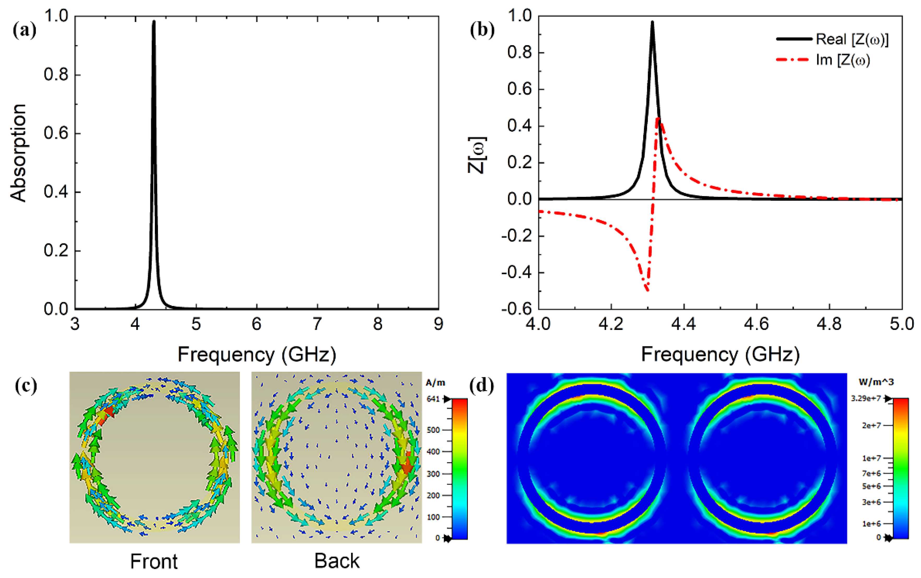
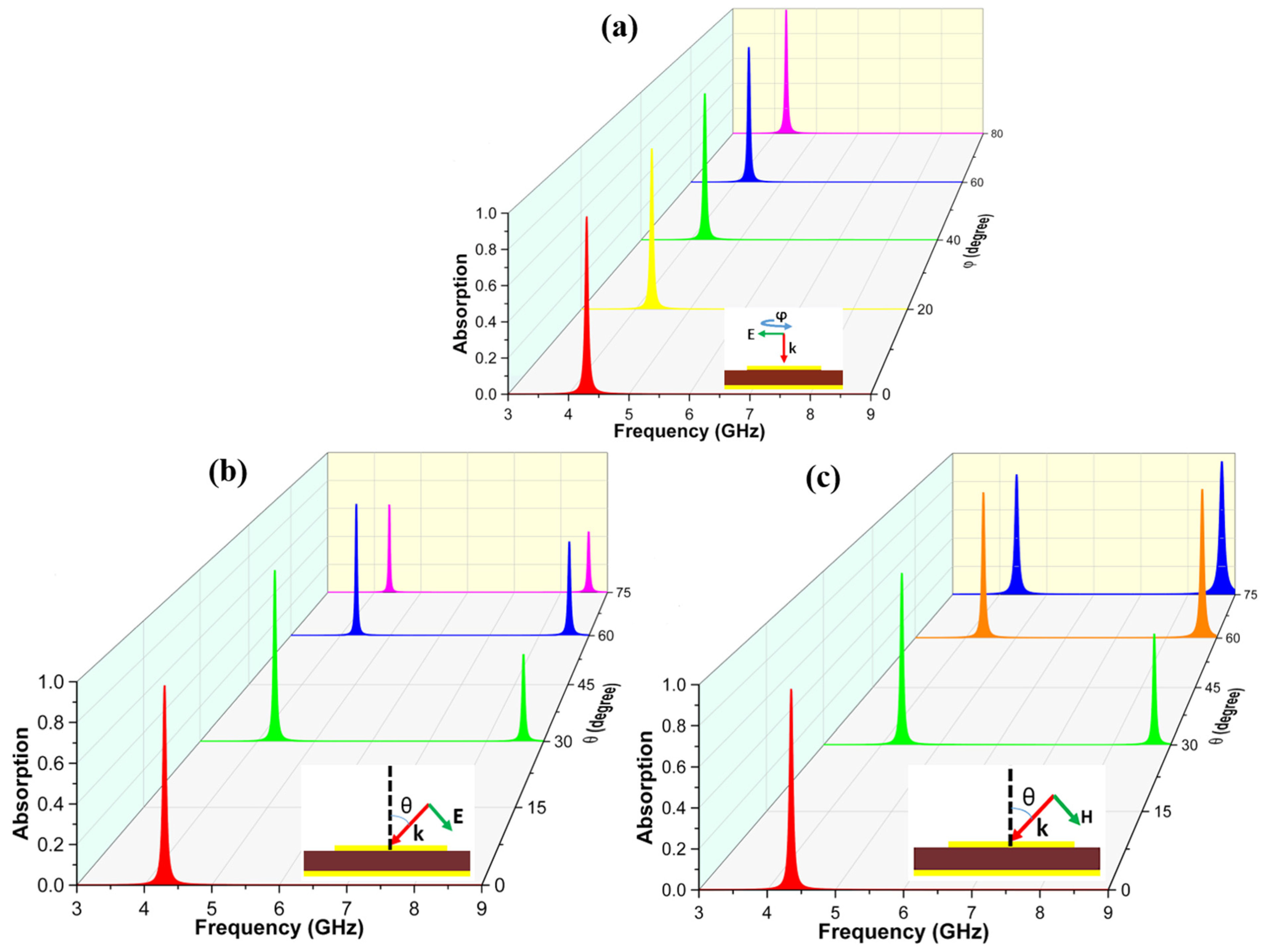
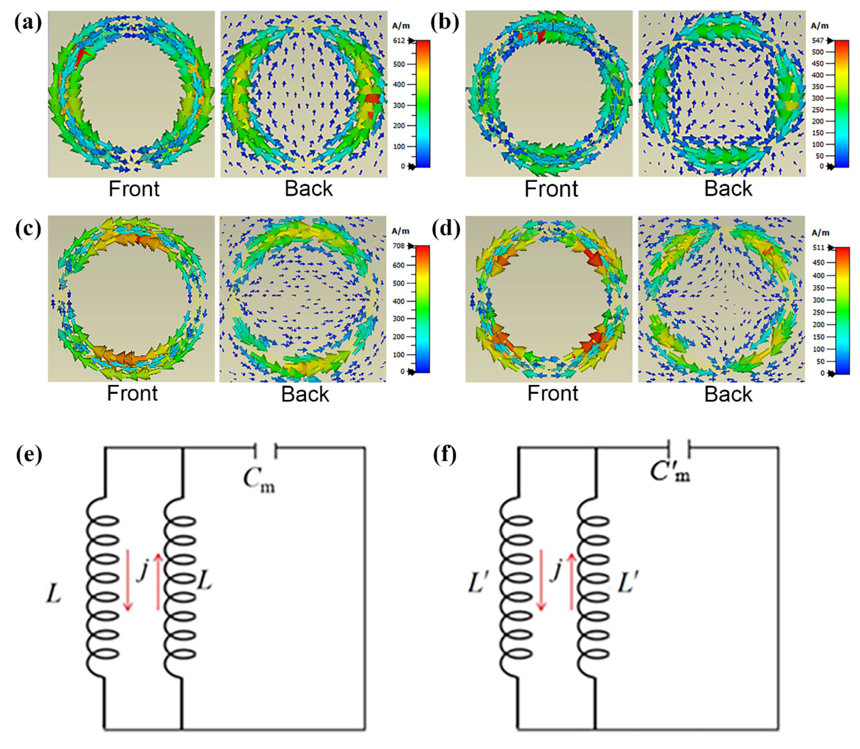
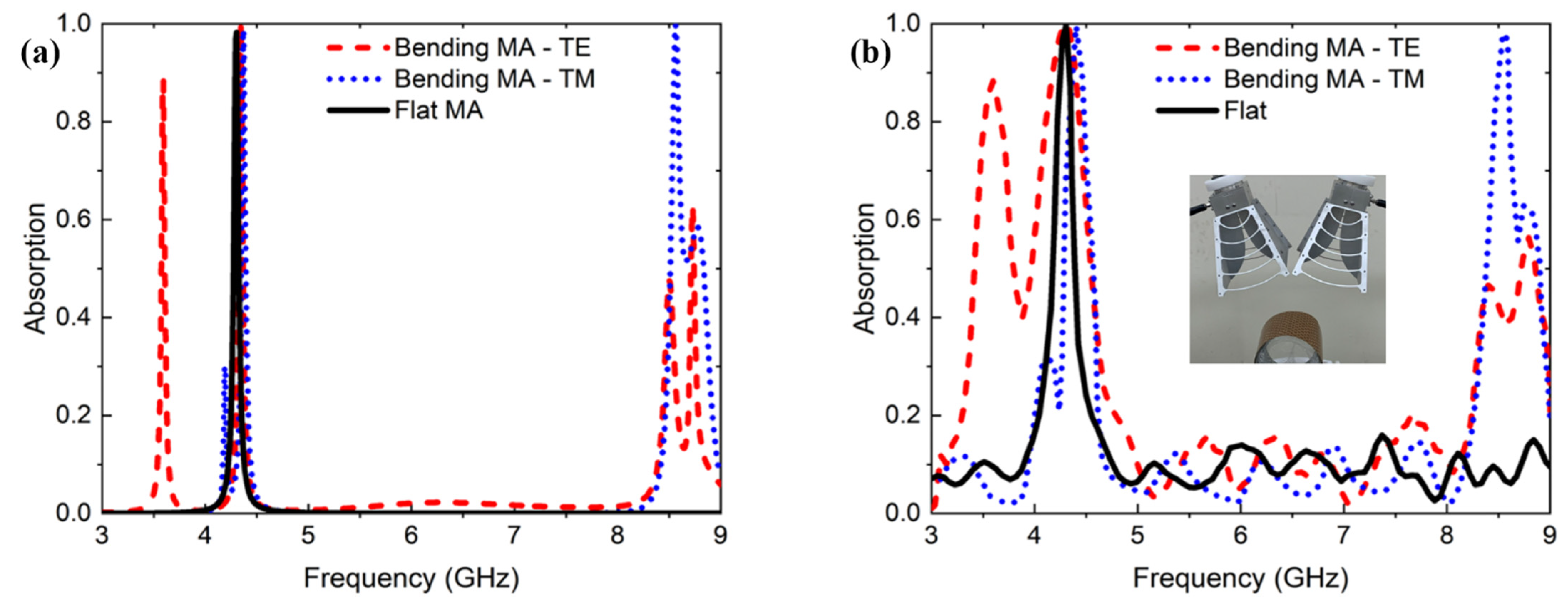
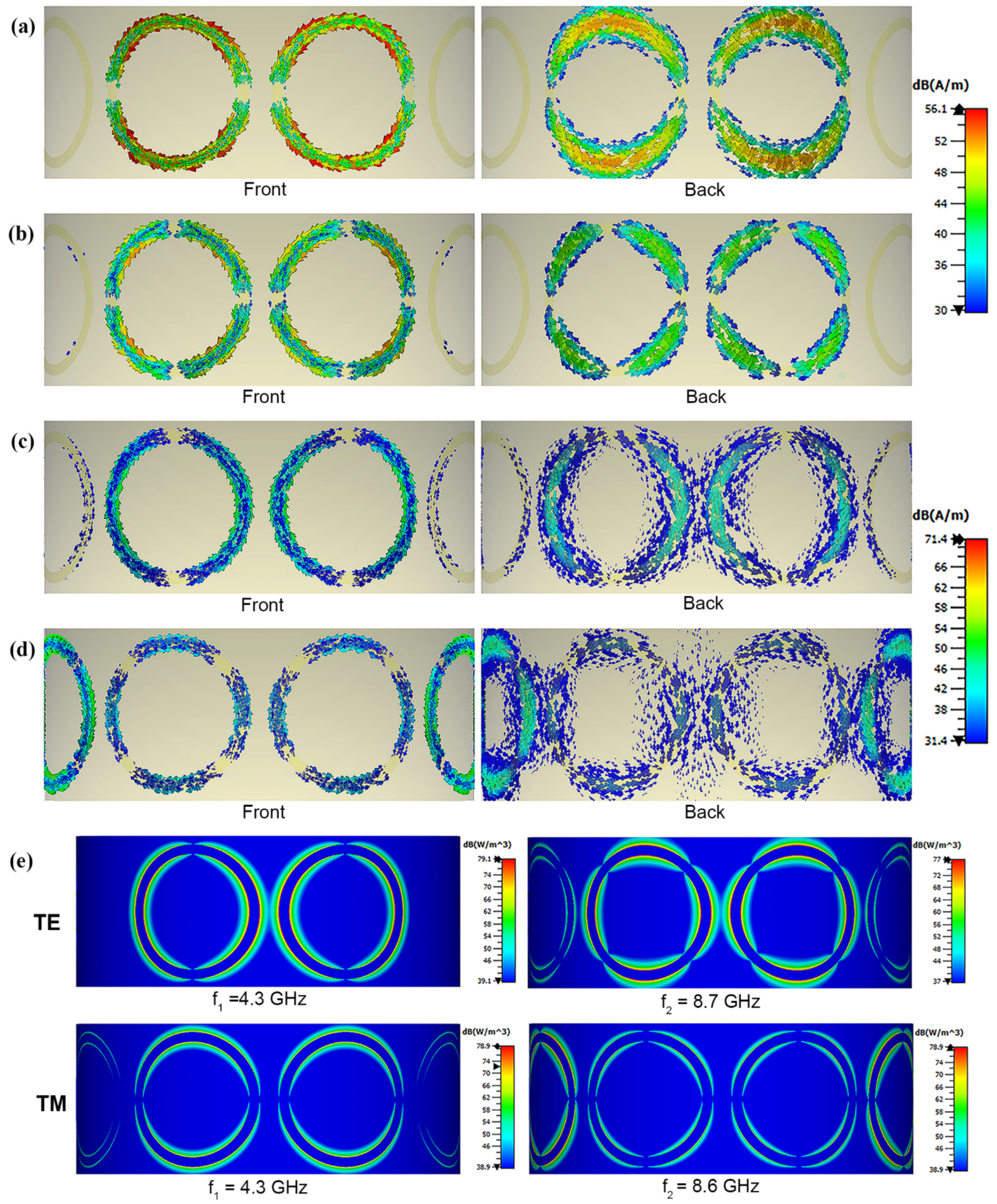
3. Results and Discussion

Firstly, we simulated the absorption of the proposed MA for the transverse-electric (TE) normal incidence in the planar configuration. The simulated result is illustrated in Figure 2a. It is clear that there is a single peak with an absorption of 98% at a frequency at 4.3 GHz. The observed phenomenon is similar to previous works, which have shown that, in general, one resonant pattern provided only a single absorption peak [31].
It is noted that the condition to achieve no reflection is the impedance matching between the structure and the free space. Thus, we also calculated the effective impedance of our MA from S parameters as follows [36]:
Z ( ω ) = ( 1 + S 11 ( ω ) ) 2 - S 21 2 ( ω ) ( 1 - S 11 ( ω ) ) 2 - S 21 2 ( ω ) .
In the case of single absorption at the normal incidence, as shown in Figure 2b, the calculated effective impedance has an imaginary part of zero and a real part of 0.96 at 4.3 GHz, which is nearly equal to the air impedance. Consequently, there is no reflection signal, and the incoming wave is absorbed into the MA at 4.3 GHz.
To analyze the nature of perfect absorption, the distribution of surface current on the metallic layers of MA was simulated for the case of TE polarization at an absorption frequency of 4.3 GHz, as in Figure 2c. It can be observed that the top and bottom surface currents are anti-parallel to each other. This means that the magnetic resonance is excited, yielding the perfect absorption at 4.3 GHz [37,38]. The power-loss density for the TE-polarized wave under the normal incidence at the resonant frequency is illustrated in Figure 2d. It is found that the high-power loss is focused mainly at the edges of the copper rings and is divided into two parts. The power-loss distribution is consistent with the charge accumulation of induced surface currents.
Figure 3a shows the simulated absorption at polarization angles varying from 0 to 80 degrees for the normal incidence. One can see that the absorption does not change when the polarization angle is varied. This demonstrates that our MPA is polarization-independent.
The influence of incidence angle on the MA performance for both TE and transverse-magnetic (TM) polarizations was studied. Figure 3b illustrates the results for TE polarization. As the incident angle increases from 0 to 60 degrees, the absorption remains higher than 90% at a frequency of 4.3 GHz. Furthermore, there is a high-order absorption occurring at 8.6 GHz and, when the oblique incidence increases to 60 degrees, the absorption reaches 63%. The appearance of this peak can be explained by the phase retardation caused by the oblique incidence [33]. When the incoming wave is not normal to the MA surface, the MA is considered to be asymmetric under the oblique incidence. The field distribution is not in phase on the whole surface. Therefore, the asymmetry of MA might lead to the excitation of a high-order dark mode at 8.6 GHz. The results for TM polarization are also presented in Figure 3c. Similar to the case of TE polarization, the fundamental peak at a frequency of 4.3 GHz is maintained well, with an absorption higher than 96% up to 60 degrees. Furthermore, the absorption of the second peak at 8.7 GHz reaches 98%. In addition, it is noteworthy that the whole thickness of the proposed structure is 0.47 mm, which is very small in respect to the absorption wavelengths, λ/148 at 4.3 GHz and λ/74 at 8.6 GHz, respectively, where λ is the corresponding operational wavelength.
To investigate the interaction mechanism of magnetic and electric components with resonators, we gave the surface-current distributions at distinct absorption frequencies for an oblique incidence of 60 degrees in the TE and TM polarization. Figure 4a,c shows the surface-current distributions at 4.3 GHz for the TE and TM polarization, respectively. Obviously, at 4.3 GHz, the front and back surface currents are anti-parallel to each other, which confirms that the absorption mechanism is affected by the magnetic resonance. The surface-current distributions at a high-order absorption frequency are shown in Figure 4b,d for the TE and TM polarization, respectively. It is observed that the current directions on the front and the back layers are still anti-parallel, indicating that the absorption is also caused by the magnetic resonance. Particularly, on both the front and back layers, the surface currents are divided into four different regions, but the currents on adjacent regions are opposite. Furthermore, the high-order absorption frequency is nearly twice the fundamental one. Therefore, it can be concluded that the higher resonance frequency is due to the second-order magnetic resonance [32,39]. The second-order magnetic resonance is generally a dark mode in the symmetric configuration. Our proposed MA structure can induce this mode because the asymmetry is developed at the oblique incidence.
The equivalent LC circuit model for the fundamental and second-order magnetic resonances are presented in Figure 4e,f. From the geometry of ring structure, one can calculate the inductance of ring L, as below:
L = ( t + 2 t m ) / 2 ( t + 2 t m ) / 2 d z [ R 1 R 2 μ 2 R 1 2 y 2 d y + R 2 R 2 μ R 1 2 y 2 2 ( R 1 R 2 ) R 1 d y + R 2 R 1 μ 2 R 1 2 y 2 d y ] = ( t + 2 t m ) μ [ π 2 arcsin R 2 R 1 + R 1 R 1 R 2 ( 1 2 arcsin R 2 R 1 + 1 2 R 2 R 1 R 1 2 R 2 2 R 1 2 ) ] ,
where µ is the free-space permeability. Then, the fundamental magnetic resonance frequency f1 can be calculated as follows:
L m = L 2 = 1 2 ( t + 2 t m ) μ [ π 2 arcsin R 2 R 1 + R 1 R 1 R 2 ( 1 2 arcsin R 2 R 1 + 1 2 R 2 R 1 R 1 2 R 2 2 R 1 2 ) ]
C m = ε 0 ε c 1 S t = ε 0 ε c 1 π ( R 1 2 R 2 2 ) t
f 1 = 1 2 π L m C m ,
where c1 is a geometrical factor of 0.2 ≤ c1 ≤ 0.3 [38], s is the area of ring, ε0 is the free-space permittivity, and ε is the polyimide permittivity.
For the second-order magnetic resonance, the distribution of surface currents on the ring is divided into two symmetric parts. Therefore, the inductance in this case is reduced as below:
L = ( t + 2 t m ) 2 t + 2 t m 2 d z [ R 2 R 1 μ 2 R 1 2 y 2 d y + 0 R 2 μ R 1 2 y 2 2 ( R 1 R 2 ) R 1 d y ] = 1 2 ( t + 2 t m ) μ [ π 2 arcsin R 2 R 1 + R 1 R 1 R 2 ( 1 2 arcsin R 2 R 1 + 1 2 R 2 R 1 R 1 2 R 2 2 R 1 2 ) ] ,
and then the inductance, capacitance and resonance frequency at the second-order peak f2 can be calculated as follows:
L m = L 2 = 1 4 ( t + 2 t m ) μ [ π 2 arcsin R 2 R 1 + R 1 R 1 R 2 ( 1 2 arcsin R 2 R 1 + 1 2 R 2 R 1 R 1 2 R 2 2 R 1 2 ) ] ,
C m = ε 0 ε c 1 S t = ε 0 ε c 1 π ( R 1 2 R 2 2 ) / 2 t
f 2 = 1 2 π L m C m
Based on these aforementioned equations, the calculated fundamental and second-order magnetic resonance frequencies are f1 = 4.3 and f2 = 8.7 GHz, respectively, which are in good agreement with the absorption frequencies observed in the simulation.
In our MA, the dielectric layer is made of polyimide, which has a great flexibility. It can be bent and attached on a cylindrical surface. In this work, we simulated and measured the absorption of a designed MA when it is bent with a bending radius of 20 mm, as shown in Figure 5. Here, for the simulation, a full structure of MA was constructed instead of the unit cell structure with unit-cell boundary. The plane-wave propagation was still directed along the z direction. For the TE-polarized wave, the electric and magnetic fields were set to be along the y and x direction, respectively. For the TM one, the conditions were reversed, with the magnetic and electric fields being in the y and x direction, respectively. For the TE polarization, three new absorption peaks appear at around 3.6, 8.5, and 8.7 GHz, with an absorption of 88%, 47%, and 62%, respectively, while the absorption of original peak at 4.3 GHz reaches 99.9%. In the case of the TM polarization, there are also three new absorption peaks at 4.2, 8.6, and 8.8 GHz, with an absorption of 30%, 99%, and 58%, respectively. The absorption of peak at 4.3 GHz reaches 99%. It can be understood that the structure becomes asymmetric by bending the MA. Therefore, both fundamental and second-order modes are excited. Differently from the effect of oblique incidence, bending the MA turns out to be extremely asymmetric, which induces four resonance peaks instead of two. For the TM mode, the bent MA is less affected. The separation between split resonances is smaller than that for the TE mode. The observed experiment results are in agreement with the simulated ones.
Figure 6 depicts the surface-current distributions for the TE and TM polarization, at different absorption frequencies. The distributions at the lower frequency are shown in Figure 6a,c, and it is observed that the resonance structures interact with the incidence wave, leading to strong surface currents in the rings at the front of cylinder. The surface currents at the front and back metallic layers are anti-parallel, which confirms that a strong magnetic resonance is made.
Figure 6b,d shows the distributions of surface current at the higher frequencies for the TE and TM polarization, respectively. In the case of the TE polarization, the strong surface currents are formed in the rings, mainly at the front of cylinder. However, in the case of the TM polarization, the surface currents are mainly at the side of cylinder. Obviously, in each ring, there are two regions in which the currents are anti-parallel, similar to the aforementioned case of oblique incidence. Figure 6e illustrates the power-loss density at different frequencies for the TE and TM polarization. At any frequency, the power losses are focused mainly on the edges of rings, which is consistent with the surface-current distribution.

4. Conclusions

We demonstrated an ultrathin flexible MA in the GHz region. In the planar model, the absorption spectrum had a single peak at a frequency of 4.3 GHz, with an absorption of 98% at the normal incidence. However, at oblique incidences, the high-order absorption peaks were achieved at 8.6 and 8.7 GHz for the TE and TM mode, respectively. Furthermore, when the proposed MA was bent with a radius of 20 mm, additional high-order absorption peaks appeared, due to the severe asymmetry of bent structure. Consequently, the dual-band MA was obtained with high absorption peaks at 3.6 (88%) and 4.3 GHz (99%) for the TE mode, while the peaks were at 4.3 (99%) and 8.6 GHz (99%) for the TM mode. The mechanism was explained by the asymmetric structure caused by phase retardation, leading to the excitation of high-order resonances. The surface-current distribution at the high-order peak indicated that the nature of this absorption peak was the second-order magnetic resonance. Our work might be exploited for a new generation of tunable devices, such as filters, sensors, and detectors.

Author Contributions

B.S.T., B.X.K., V.D.L. and Y.L. conceived the idea. The electromagnetic simulations and calculations were carried out by D.T.H., B.S.T., B.X.K., H.Z. and N.T.T. The experiments were carried out by D.T.H., B.S.T., N.H.T., N.T.H. and T.S.P., B.S.T., B.X.K., L.Y.C., Y.L. and V.D.L. analyzed and wrote the article. All of the authors discussed and commented on the manuscript. All authors have read and agreed to the published version of the manuscript.

Funding

This research is funded by the Vietnam Academy of Science and Technology, under grant numbers KHCBVL.01/20-21 and NCVCC42.03/21-21, and by the Korea Evaluation Institute of Industrial Technology (Project No. 20016179).

Institutional Review Board Statement

Not applicable.

Informed Consent Statement

Not applicable.

Data Availability Statement

The data presented in this paper are available on request from the corresponding author.

Conflicts of Interest

The authors declare no conflict of interest.

References

  1. Sreekanth, K.V.; Alapan, Y.; ElKabbash, M.; Ilker, E.; Hinczewski, M.; Gurkan, U.A.; Luca, A.D.; Strangi, G. Extreme sensitivity biosensing platform based on hyperbolic metamaterials. Nat. Mater. 2016, 15, 621–627. [Google Scholar] [CrossRef] [PubMed] [Green Version]
  2. Palermo, G.; Sreekanth, K.V.; Maccaferri, N.; Lio, G.E.; Nicoletta, G.; Angelis, F.D.; Hinczewski, M.; Strangi, G. Hyperbolic dispersion metasurfaces for molecular biosensing. Nanophotonics 2021, 10, 295–314. [Google Scholar] [CrossRef]
  3. Ma, L.; Chen, D.; Zheng, W.; Li, J.; Zahra, S.; Liu, Y.; Zhou, Y.; Huang, Y.; Wen, G. Advanced electromagnetic metamaterials for temperature sensing applications. Front. Phys. 2021, 9, 195. [Google Scholar] [CrossRef]
  4. Liao, Y.L.; Zhao, Y. Ultra-narrowband dielectric metamaterial absorber with ultra-sparse nanowire grids for sensing applications. Sci. Rep. 2020, 10, 1–7. [Google Scholar]
  5. Montoya, J.A.; Tian, Z.B.; Krishna, S.; Padilla, W.J. Ultra-thin infrared metamaterial detector for multicolor imaging applications. Opt. Express 2017, 25, 23343–23355. [Google Scholar] [CrossRef]
  6. Haxha, S.; AbdelMalek, F.; Ouerghi, F.; Charlton, M.D.B.; Aggoun, A.; Fang, X.J.S.R. Metamaterial superlenses operating at visible wavelength for imaging applications. Sci. Rep. 2018, 8, 1–15. [Google Scholar]
  7. Karaaslan, M.; Bağmancı, M.; Ünal, E.; Akgol, O.; Sabah, C. Microwave energy harvesting based on metamaterial absorbers with multi-layered square split rings for wireless communications. Opt. Commun. 2017, 392, 31–38. [Google Scholar] [CrossRef]
  8. Alkurt, F.O.; Altintas, O.; Ozakturk, M.; Karaaslan, M.; Akgol, O.; Unal, E.; Sabah, C. Enhancement of image quality by using metamaterial inspired energy harvester. Phys. Lett. A 2020, 384, 126041. [Google Scholar] [CrossRef]
  9. Landy, N.I.; Sajuyigbe, S.; Mock, J.J.; Smith, D.R.; Padilla, W.J. Perfect metamaterial absorber. Phys. Rev. Lett. 2008, 100, 207402. [Google Scholar] [CrossRef]
  10. Yoo, Y.J.; Zheng, H.Y.; Kim, Y.J.; Rhee, J.Y.; Kang, J.H.; Kim, K.W.; Cheong, H.; Kim, Y.H.; Lee, Y. Flexible and elastic metamaterial absorber for low frequency, based on small-size unit cell. Appl. Phys. Lett. 2014, 105, 041902. [Google Scholar] [CrossRef]
  11. Khuyen, B.X.; Tung, B.S.; Kim, Y.J.; Hwang, J.S.; Kim, K.W.; Rhee, J.Y.; Lam, V.D.; Kim, Y.H.; Lee, Y. Ultra-subwavelength thickness for dual/triple-band metamaterial absorber at very low frequency. Sci. Rep. 2018, 8, 1–9. [Google Scholar] [CrossRef] [Green Version]
  12. Lio, G.E.; Ferraro, A.; Giocondo, M.; Caputo, R.; De Luca, A. Color gamut behavior in epsilon near-zero nanocavities during propagation of gap surface plasmons. Adv. Opt. Mater. 2020, 8, 2000487. [Google Scholar] [CrossRef]
  13. Zhong, M. Design and measurement of a narrow band metamaterial absorber in terahertz range. Opt. Mater. 2020, 100, 109712. [Google Scholar] [CrossRef]
  14. Cheng, Y.; Yang, H.; Cheng, Z.; Wu, N. Perfect metamaterial absorber based on a split-ring-cross resonator. Appl. Phys. A 2011, 102, 99–103. [Google Scholar] [CrossRef]
  15. Assimonis, S.D.; Fusco, V. Polarization insensitive, wide-angle, ultra-wideband, flexible, resistively loaded, electromagnetic metamaterial absorber using conventional inkjet-printing technology. Sci. Rep. 2019, 9, 1–15. [Google Scholar]
  16. Elsharabasy, A.; Bakr, M.; Deen, M.J. Wide-angle, wide-band, polarization-insensitive metamaterial absorber for thermal energy harvesting. Sci. Rep. 2020, 10, 1–10. [Google Scholar] [CrossRef]
  17. Liu, J.; Ma, W.Z.; Chen, W.; Yu, G.X.; Chen, Y.S.; Deng, X.C.; Yang, C.F. Numerical analysis of an ultra-wideband metamaterial absorber with high absorptivity from visible light to near-infrared. Opt. Express 2020, 28, 23748–23760. [Google Scholar] [CrossRef]
  18. Liu, H.; Wang, Z.H.; Li, L.; Fan, Y.X.; Tao, Z.Y. Vanadium dioxide-assisted broadband tunable terahertz metamaterial absorber. Sci. Rep. 2019, 9, 1–10. [Google Scholar]
  19. Hu, F.; Wang, L.; Quan, B.; Xu, X.; Li, Z.; Wu, Z.; Pan, X. Design of a polarization insensitive multiband terahertz metamaterial absorber. J. Phys. D Appl. Phys. 2013, 46, 195103. [Google Scholar] [CrossRef]
  20. Wang, W.; Wang, K.; Yang, Z.; Liu, J. Experimental demonstration of an ultra-flexible metamaterial absorber and its application in sensing. J. Phys. D Appl. Phys. 2017, 50, 135108. [Google Scholar] [CrossRef]
  21. Sadeqi, A.; Nejad, H.R.; Sonkusale, S. Low-cost metamaterial-on-paper chemical sensor. Opt. Express 2017, 25, 16092–16100. [Google Scholar] [CrossRef] [PubMed]
  22. Tasolamprou, A.C.; Mentzaki, D.; Viskadourakis, Z.; Economou, E.N.; Kafesaki, M.; Kenanakis, G. Flexible 3D printed conductive metamaterial units for electromagnetic applications in microwaves. Materials 2020, 13, 3879. [Google Scholar] [CrossRef]
  23. Borah, D.; Bhattacharyya, N.S. Design, fabrication and characterization of flexible and ultrathin microwave metamaterial absorber. In Proceedings of the 2017 International Conference on Innovations in Electronics, Signal Processing and Communication (IESC), Shillong, India, 6–7 April 2017; pp. 190–193. [Google Scholar]
  24. Amiri, M.; Tofigh, F.; Shariati, N.; Lipman, J.; Abolhasan, M. Wide-angle metamaterial absorber with highly insensitive absorption for TE and TM modes. Sci. Rep. 2020, 10, 1–13. [Google Scholar] [CrossRef]
  25. Song, Z.; Wang, K.; Li, J.; Liu, Q.H. Broadband tunable terahertz absorber based on vanadium dioxide metamaterials. Opt. Express 2018, 26, 7148–7154. [Google Scholar] [CrossRef]
  26. Bai, J.; Zhang, S.; Fan, F.; Wang, S.; Sun, X.; Miao, Y.; Chang, S. Tunable broadband THz absorber using vanadium dioxide metamaterials. Opt. Commun. 2019, 452, 292–295. [Google Scholar] [CrossRef]
  27. Ma, J.; Wang, J.; Hu, Z.D.; Zhang, Z.; Pan, L.; Di Falco, A. High-efficiency and ultrabroadband flexible absorbers based on transversely symmetrical multi-layer structures. AIP Adv. 2019, 9, 115007. [Google Scholar] [CrossRef] [Green Version]
  28. Yang, D.; Xia, Y. Experimental verification of multi-band metamaterial absorber with double structured layers. Mater. Res. Express 2020, 7, 035801. [Google Scholar] [CrossRef]
  29. Zhao, L.; Liu, H.; He, Z.; Dong, S. Theoretical design of twelve-band infrared metamaterial perfect absorber by combining the dipole, quadrupole, and octapole plasmon resonance modes of four different ring-strip resonators. Opt. Express 2018, 26, 12838–12851. [Google Scholar] [CrossRef]
  30. Wang, J.; Lang, T.; Hong, Z.; Xiao, M.; Yu, J. Design and fabrication of a triple-band terahertz metamaterial absorber. Nanomaterials 2021, 11, 1110. [Google Scholar] [CrossRef] [PubMed]
  31. Jung, S.; Kim, Y.J.; Yoo, Y.J.; Hwang, J.S.; Khuyen, B.X.; Chen, L.Y.; Lee, Y. High-order resonance in a multiband metamaterial absorber. J. Electron. Mater. 2020, 49, 1677–1688. [Google Scholar] [CrossRef]
  32. Huang, X.; Lu, C.; Rong, C.; Hu, Z.; Liu, M. Multiband ultrathin polarization-insensitive terahertz perfect absorbers with complementary metamaterial and resonator based on high-order electric and magnetic resonances. IEEE Photonics J. 2018, 10, 1–11. [Google Scholar] [CrossRef]
  33. Khuyen, B.X.; Tung, B.S.; Tung, N.T.; Hien, N.T.; Kim, Y.J.; Chen, L.Y.; Lee, Y.; Linh, P.T.; Lam, V.D. Realization for dual-band high-order perfect absorption, based on metamaterial. J. Phys. D Appl. Phys. 2019, 53, 105502. [Google Scholar] [CrossRef]
  34. Nguyen, T.H.; Nguyen, T.A.H.; Dinh, T.N.; Bui, X.K.; Bui, S.T.; Nguyen, X.C.; Nguyen, B.T.; Vu, D.L. Multiband metamaterial absorber in a ring structure base on high-order magnetic resonance. Commun. Phys. 2021, 31, 199. [Google Scholar] [CrossRef]
  35. CST Microwave Studio 2015, License ID: 52856-1. Dassault Systèmes. Available online: http://www.cst.com (accessed on 15 June 2021).
  36. Chen, X.; Grzegorczyk, T.M.; Wu, B.-I.; Pacheco, J., Jr.; Kong, J.A. Robust method to retrieve the constitutive effective parameters of metamaterials. Phys. Rev. E 2004, 70, 016608. [Google Scholar] [CrossRef] [Green Version]
  37. Nguyen, T.Q.H.; Nguyen, T.K.T.; Cao, T.N.; Nguyen, H.; Bach, L.G. Numerical study of a broadband metamaterial absorber using a single split circle ring and lumped resistors for X-band applications. AIP Adv. 2020, 10, 035326. [Google Scholar] [CrossRef]
  38. Zhou, J.; Economon, E.N.; Koschny, T.; Soukoulis, C.M. Unifying approach to left-handed material design. Opt. Lett. 2006, 31, 3620–3622. [Google Scholar] [CrossRef] [PubMed]
  39. Cheng, Y.Z.; Cheng, Z.Z.; Mao, X.S.; Gong, R.Z. Ultra-thin multi-band polarization-insensitive microwave metamaterial absorber based on multiple-order responses using a single resonator structure. Materials 2017, 10, 1241. [Google Scholar] [CrossRef] [Green Version]
Figure 1. (a) Schematic of the unit cell of the proposed metamaterial absorber (MA), (b) top view, (c) measurement configuration, and (d) S-parameter formation.
Photonics 08 00574 g001
Figure 2. (a) Absorption spectrum of MA, (b) effective impedance, (c) surface-current distribution on the metallic layers of MA, and (d) power-loss density.
Photonics 08 00574 g002
Figure 3. Simulated absorption as a function of (a) polarization angle (φ) and (b) incidence angle (θ) for the TE polarization. (c) Simulated absorption according to incidence angle for the TM polarization.
Photonics 08 00574 g003
Figure 4. Surface currents at a frequency of (a) 4.3 and (b) 8.6 GHz in the TE mode; (c) those at a frequency of 4.3 and (d) 8.7 GHz in the TM mode. Equivalent circuit models of (e) the fundamental resonance and (f) the second-order magnetic one.
Photonics 08 00574 g004
Figure 5. (a) Simulated and (b) measured absorption spectra of flat MA and bent MA for the TE and TM polarizations. The inset illustrates the schematic of absorption measurement when the MA is bent.
Photonics 08 00574 g005
Figure 6. Surface-current distributions and power loss density of bent MA for the TE and TM polarization for the normal incidence and a bending radius of 20 mm at different resonance frequencies. for the TE polarization at a frequency of (a) 4.3 and (b) 8.7 GHz; surface-current distributions for the TM polarization at a frequency of (c) 4.3 and (d) 8.6 GHz. (e) Power loss density of the bent MA for the TE and TM polarization at different frequencies.
Photonics 08 00574 g006
Publisher’s Note: MDPI stays neutral with regard to jurisdictional claims in published maps and institutional affiliations.

