1. Introduction
A polarized electron-ion collider (EIC) is a planned tool for gluon microscopy to explore the frontiers of quantum chromo-dynamics [
1]. The EIC lepton-hadron collider concept is targeting ultra-high luminosities of 10
34 cm
−2 s
−1, approaching those in lepton-lepton colliders [
2]. In order to deliver such high luminosities, a scheme to use multi-stage electron cooling of the ion beam has been developed by the Thomas Jefferson National Accelerator Facility (JLAB) [
3]. In this approach the ion beam is first electron-cooled at low energy to reduce the emittance, and then is accelerated to the collision energy where electron cooling is again continuously reapplied to maintain luminosity during collisions, by suppressing emittance degradation due to non-linear collective effects plus intra-beam and residual gas scattering processes.
However, ionization scattering of the electron beam with residual gas molecules causes ion trapping in the electron rings, both in the collider and electron-cooling system [
4]. These trapped ions may cause emittance growth, tune shift, halo formation, and coherent coupled bunch instabilities [
5,
6]. Therefore, the beam’s temporal structure needs clearing gaps for timely removal of the residual ions to prevent them from accumulating over many turns. Typically, the gap in the bunch train has a length of a few percent of the net ring circumference [
7], so the clearing voltage has to be applied within that interval.
Even with improvements in vacuum technology, ions can fully neutralize the electron beam within seconds for vacuum pressures as low as 10
−9 Torr [
8]. Therefore, it is necessary to directly remove the trapped ions in order to avoid or mitigate these unwanted effects. Ion-clearing methods are understood well enough to mitigate ion effects in most storage rings and synchrotrons [
9,
10]. In low repetition rate linacs, ion trapping is typically not observed, because the ions have enough time to drift out of the center of the beam pipe between bunches.
With superconducting linacs operating in a continuous wave (c.w.) high current regime [
11], the ion trapping is unavoidable [
6] and needs to be mitigated. Examples include: strong electron cooling in JLab-proposed EIC [
12], Cornell Energy Recovery Linac (ERL) [
13], and electron-cooling of ion beam at low energies of 7.7–20 GeV/nucleon in The Relativistic Heavy Ion Collider (RHIC) [
14]. With no ion-clearing mechanisms, the ion density would increase until reaching that of the electrons. Therefore, an ion-clearing gap system can be used to reduce trapped ions into the electron beam time structure. In general, such a system includes an in-vacuum electromagnetic deflector (sometimes called “kicker”), a beam dump, and corresponding electronics that provide the waveform of appropriate shape, repetition rate, timing, and magnitude (related to peak and average power).
In response to this problem RadiaBeam, in collaboration with JLAB scientists, is developing an ultra-fast high-voltage (HV) kicker. The system is designed to kick out four of 31 bunches, while keeping the rest in the bunch train, at 43.4 MHz base bunch rep rate to leave a gap of ~92–100 ns (see
Figure 1). This design satisfies the following requirements, summarized in
Table 1: 20 mrad deflecting angle at 7 MeV/c beam momentum, deflector length less than 1 m, gap duration ~100 ns, and 1.397 MHz repetition rate (phase locked). Both the rise and fall time of the deflecting pulses must be less than 20 ns (<10 ns desirable for rise time), with a sub-ns or better timing jitter. The clearing system does not perturb the quality of the beam pulses injected into the linac; it also avoids creating a substantial halo, which must remain <10
−5 of the beam current. In this paper, we will report the kicker’s electromagnetic design, and the initial tests of several high-voltage switches and pulse-forming schemes.
2. Electromagnetic Design
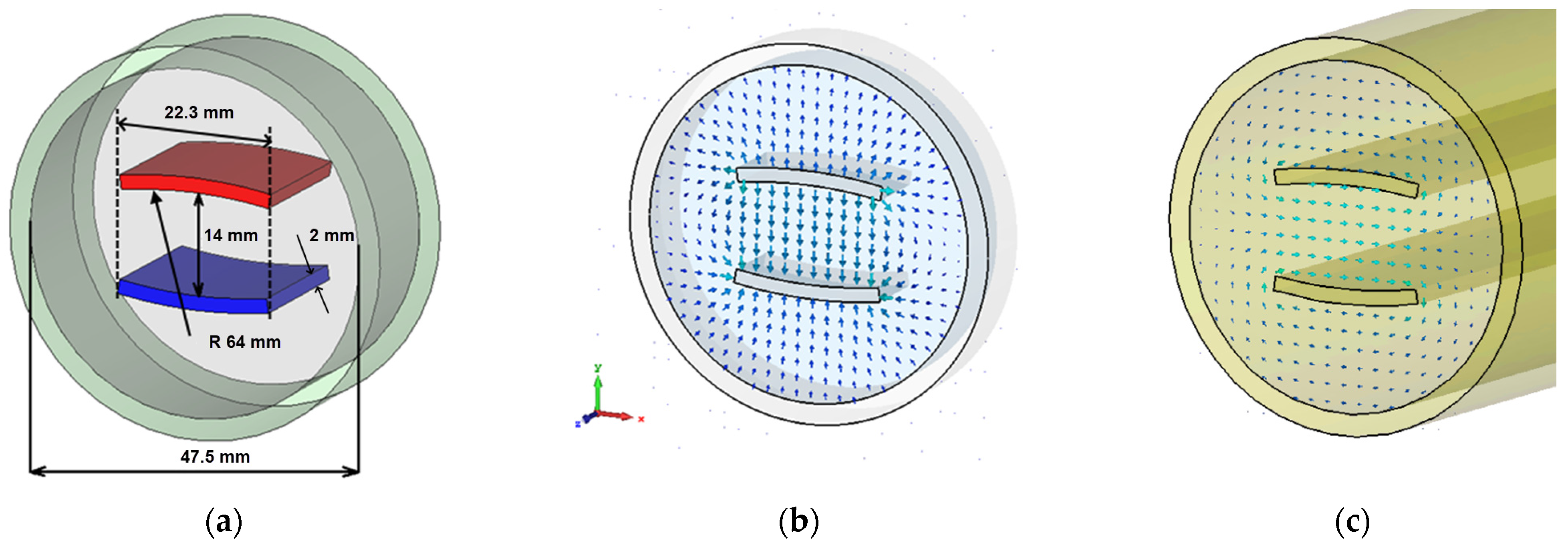
Figure 2 demonstrates the electromagnetic model of the kicker, used for the simulations in CST Microwave Studio. The kicker is formed with two parallel electrodes inside a vacuum chamber (Ø47.5 mm pipe matching existing JLAB beamline) and four 50 Ω coaxial ports, two of which serve as power inputs and two are terminated with matching 50 Ω water-cooled loads. The design process was carried out centrally focused around two main aspects: RF behavior and beam dynamics.
As a four-port RF device, the kicker must be able to provide matching across a bandwidth of at least 0–200 MHz to ensure no distortion in the form of the 10 ns rise and fall times of 92 ns-long rectangular pulses. This requirement transforms into the following condition: the stripline, consisting of two parallel electrodes inside a pipe, must represent a transmission line with 100 Ω characteristic impedance at an odd mode; given that the structure is excited with 180° out-of-phase pulses through two 50 Ω inputs. There are two reasons why a 100 Ω impedance is chosen: one is because there is a minimum gap (14 mm) between the electrodes that is driven by the beam rms size (σr = 1 mm, ±6σr); the other is simply because it is reasonable to stick with commercially available 50 Ω components, e.g., rigid coaxial lines and high-power loads.
By adjusting the electrodes widths and their curvature radius, we have optimized their shapes to both show 100 Ω characteristic impedance at the odd mode and uniform field around the axis within ±6
σr radius (
σr = 1 mm), as shown in
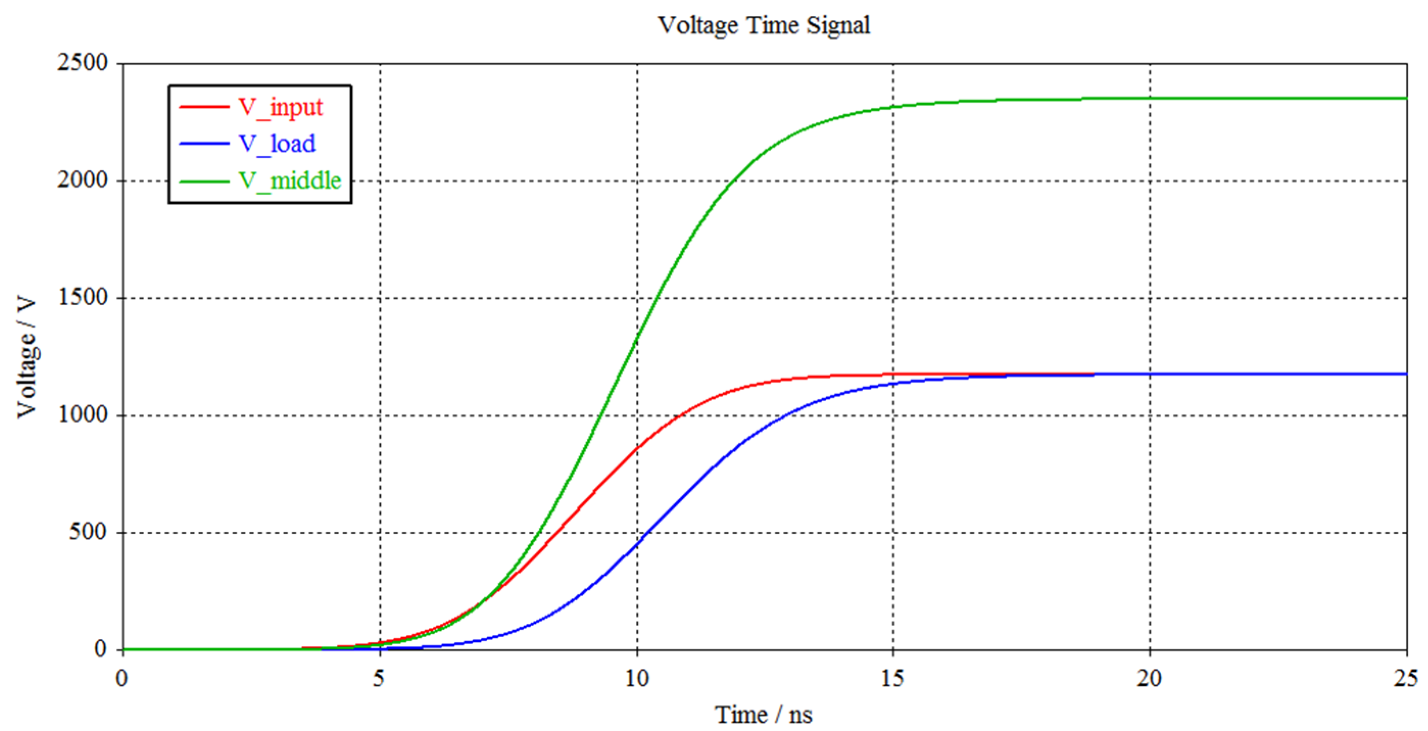
Figure 3. In order to validate how well the impedance-matched kicker conducts the 10 ns rise times, we ran time-domain simulations while monitoring the pulse shapes at the input ports, in the middle of the structure and at the loads. Simulated waveforms are plotted in
Figure 4. From this plot, it is possible to see that the proposed kicker geometry does not distort the operation pulse shape.
The required deflecting voltage can be calculated using the following expression:
Here
y’ is a deflection angle,
p is particle’s momentum. For the given
pz = 7 MeV/
c, the results in the required deflection voltage of
Vy = 140 kV. Vertical deflection is provided by both electric (
Ey) and magnetic (
Bx) components of the field:
For 7 MeV electrons their normalized velocity is β
= v/c = 0.997.
Leff is the kicker effective interaction length. Note, that the two forces will add with one beam direction, and ‘cancel’ each other with the opposite. The ratio of contributions to the deflection from electric over magnetic forces for a given stripline and loads impedances is ~1:1, which gives the estimation of voltage pulse amplitude per port:
From this expression we can calculate the total input power, dissipated in two loads, required to provide 20 mrad deflection:
Here
RLoad is a 50 Ω load impedance and the gap width (
g) is considered to be predefined (14 mm), so the kicker length is the main parameter that will drive the power requirement. The plot in
Figure 5 shows the peak and average power consumption dependence on the kicker length.
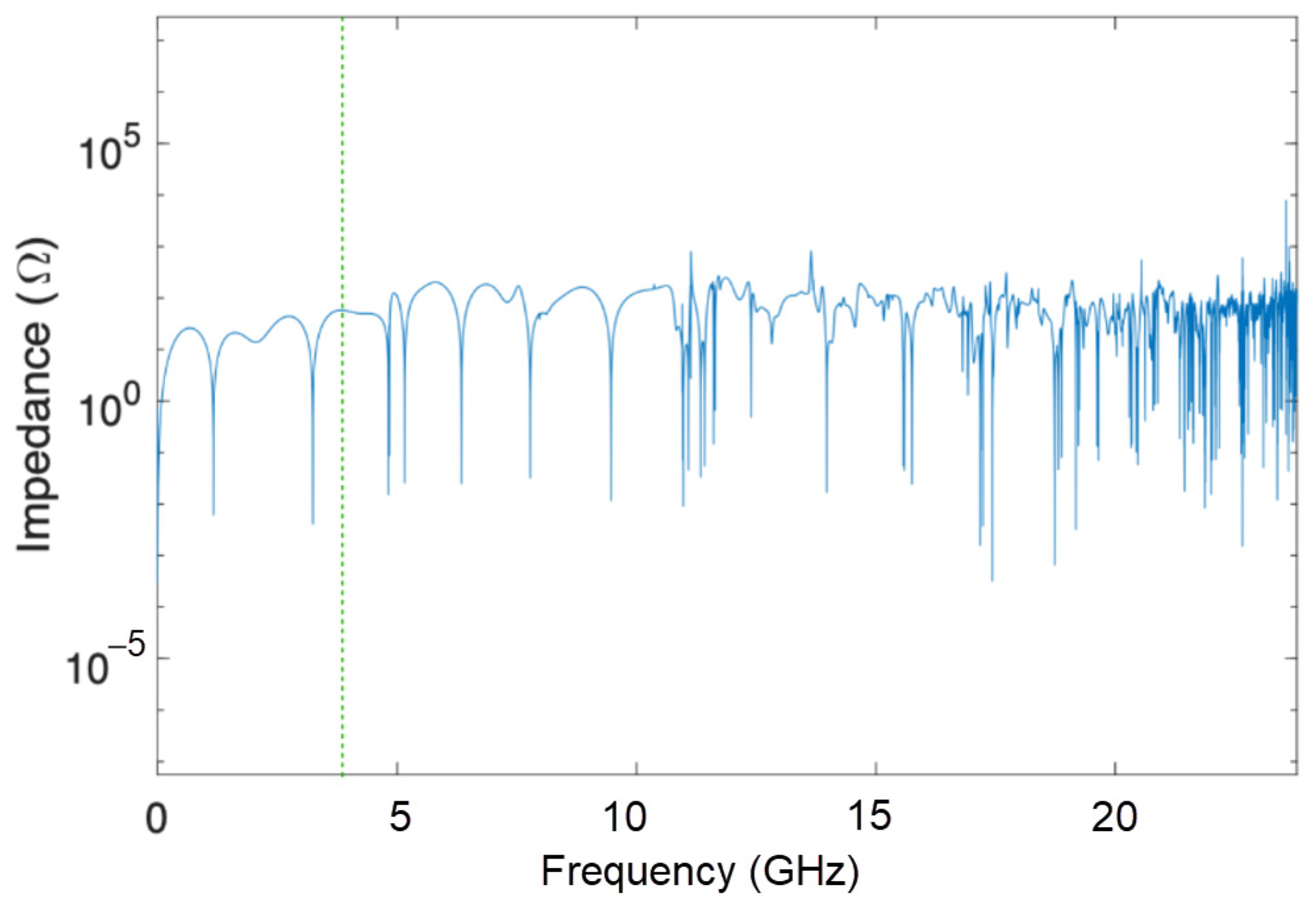
The wakefields of the kicker cavity, which can be excited by the passing electron beam and could cause excessive heat on the cavity wall or degradation of the beam quality, was studied by using CST Particle Studio (wakefield solver). In particular, the heating comes from the trapped modes within the cavity below the cutoff frequency of TE
11-mode in the beam pipe, which is about 3.7 GHz. The impedance spectrum over the broadband (up to 25 GHz) is shown in
Figure 6 by using fast Fourier transform (FFT) code for accurate evaluation from the wakefields. As shown in this plot, the impedance remains roughly constant over frequency at low values of 10~100 Ω, which would imply about 0.5 W level of associated heating for JLab EIC operation. It is also expected that this low impedance would translate into minimal effect on beam quality throughout the beam pipe.
3. Beam Dynamics
To this point, we estimated the required voltage and kicker length from the specified nominal deflection without taking into account the bunch size. In a proposed operation of the stripline kicker cavity at JLAB [
15], there is a tight constraint on the beam loss rate due to a relatively large bunch charge. A shorter cavity implies less beam loss but higher RF power requirements. Therefore, the length of the stripline kicker must be optimized so that the electron bunches go through the cavity without significant beam loss. At the same time, the RF power requirement should be minimized as much as possible. It is also noted that the beam loss can be controlled not only by the cavity length but also by the initial injection angle and position of the beam. In practice, the requirement for beam losses is set as less than a couple of W/m. Therefore, the optimization process is reduced to obtaining the minimum RF power.
In order to find an optimal choice for the kicker cavity length, we consider a series of lengths to check on the beam loss over a range of injection beam parameters. Then, the length would be determined for the case with the lowest corresponding RF power. Since simulating a range of injection parameters directly would have been very time consuming, we instead calculated an analytical description of the beam trajectories and then benchmarked the simulation results by the CST Particle Studio particle-in-cell [
16] (PIC) solver for only a few cases. With a reasonable agreement between the two approaches, we found the optimal injection parameters based on the analytical computation and subsequently used the choice to undertake a final simulation in order to predict the beam loss and the RF power of the cavity.
The equation of motion for an electron bunch in y-direction is given as:
where
Fy is a Coulomb and Lorentz forces from (2) and can be written as
Fy = 4
Vp/
g with
Vp and
g being kick voltage and gap width, respectively. The solution within a stripline is trivially obtained with a constant
Fy:
where
C =
Fy/
mγ
2, which describes a parabola. With the initial vertical velocity
v0 < 0, the tip location of the parabola is given by differentiating Equation (6) with respect to
z:
The trajectory over a whole kicker cavity, assuming there is no force between the edge of kicker cavity and the stripline is given as:
where
Leff is the length of stripline and
l is the additional length to kicker cavity ends. In particular, the
y-offset at the exit of the stripline kicker
Y is given as:
Now, the distance between the edge of the gap and the center of beam, (
g/2-
Y) defines to beam loss
R in Gaussian transverse profile of the beam (only on one side) as follows:
where
σ is transverse rms size of the beam (1 mm). This would lead to the beam loss power as:
Here
fb,
Qb, and
W are, respectively: bunch frequency, bunch charge, and electron energy. For the JLab EIC
Qb = 1.6 nC and
fb = 43.3 MHz, and
W = 7 MeV, yielding the required powers, provided in
Table 1.
The equation of motion (6) for an unkicked bunch becomes trivial with C = 0 (Fy = 0). The offset Yu at the end of the stripline is simply given as Yu = y0 + v0Leff/c and again the corresponding beam loss Ru and power are obtained similarly by (11) and (12). On the other hand, the required power scales as P = Vp2/g. Here VpLeff/g is held constant for a fixed deflection angle, leading to P scaling as ~1/Leff2. We avoid changing the gap (g) which will change impedance matching.
The comparison between the theoretical computations and the numerical simulations using the CST Particle is made (see
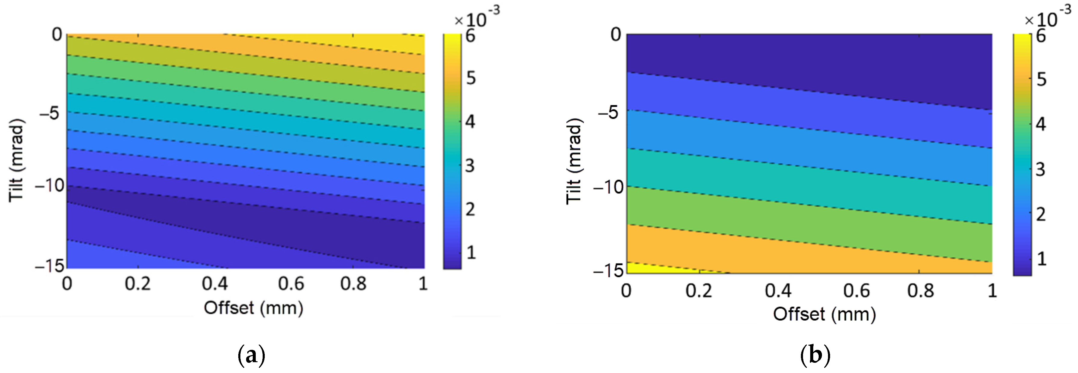
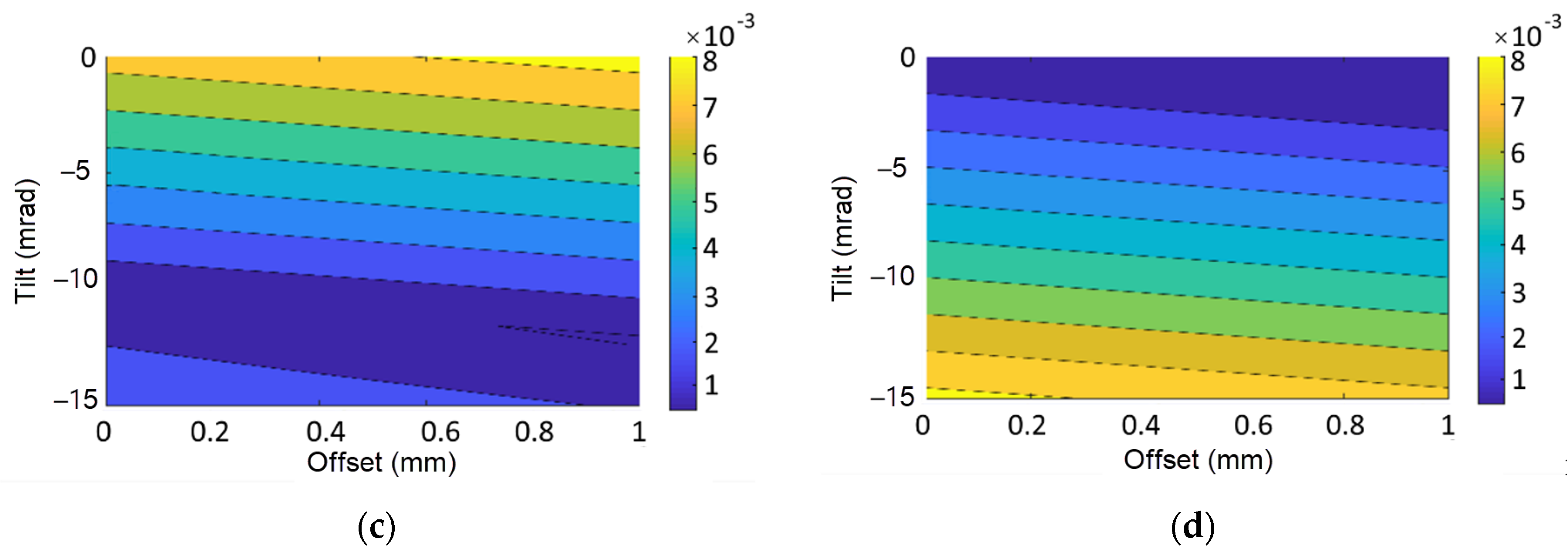
Table 2). For a given set of cavities with lengths of 200–600 mm, the simulations with injection parameters of 0 mm offset and 0 mrad tilting were undertaken (without space charge effects) and benchmarked by the analytical results. With relatively good agreements between the two, we used analytical evaluation to find optimal injection parameters for minimum beam loss with various cavity lengths. We obtained a spectrum of beam loss over a range of injection parameters–offset and tilting–as shown in
Figure 7.
From this study, it is clear that the optimal injection parameters range between 5~6 mrad tilting and near 0 mm offset regardless of cavity length. Considering the required pulsed power, it was decided that either 400 mm or 500 mm cavity would be close to the optimal choice, i.e., reasonably low RF power with tolerable beam loss, which was confirmed by the CST simulation. Finally, space charge effect was added to give a more realistic prediction on beam loss. This choice would imply the tilting of the kicker cavity by moving the tail of the cavity by about 5 mm with respect to beam axis, which can be easily controlled.
4. High-Voltage Tests
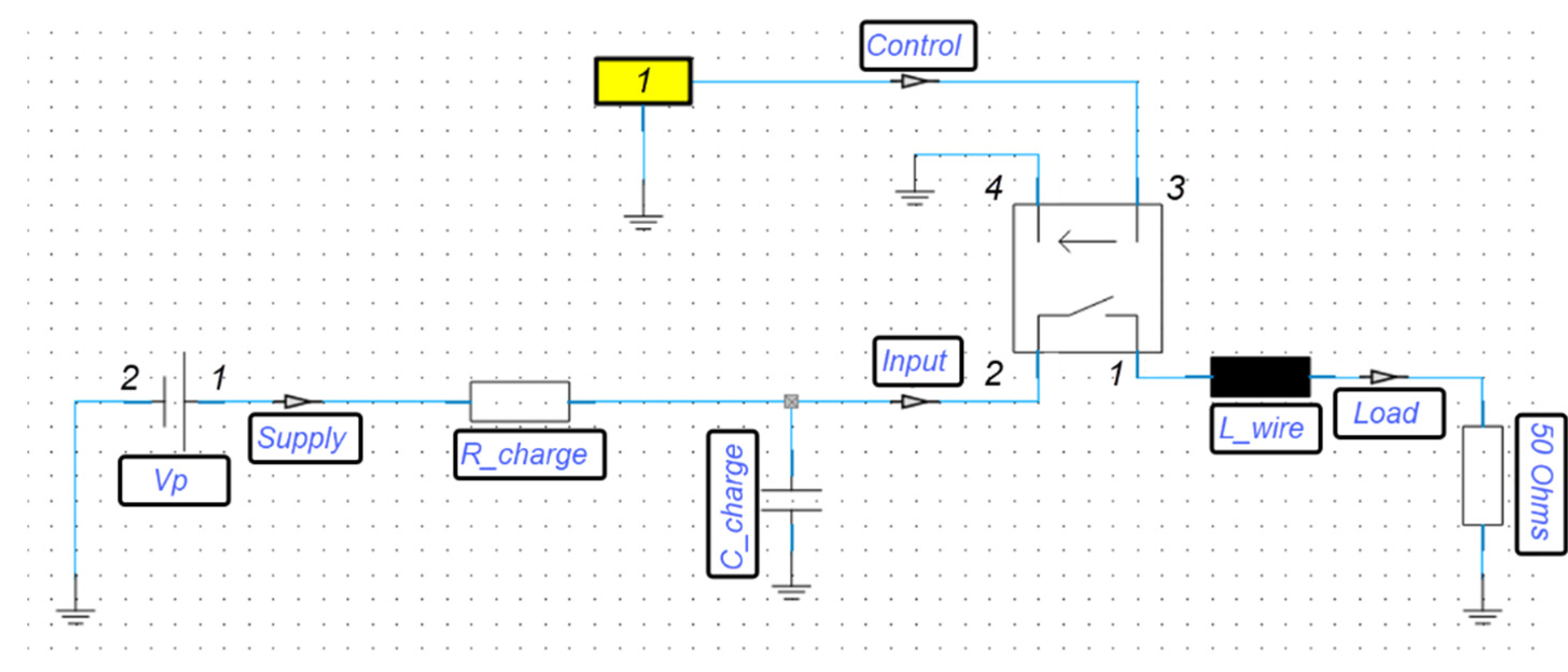
Our main goal in performing HV modulator experimental work is to test the associated critical components. We consider the switches to be the key element of most pulse-forming devices regardless of their principal schemes. The primary goal of the tests was to confirm that 10 ns rise and fall times are achievable, the switch is capable of changing its state at the desired 1.4 MHz rep rate with 100 ns flat-top duration, and that it can conduct high currents without overheating. In order to test the switch, we fabricated a test stripline as shown in
Figure 8, so that it mimics one half of the kicker structure. Essentially, the stripline is a 50 cm-long piece of 50 Ω line with 1–5/8″ coaxial connectors. We also attached a 50 Ω coaxial load rated to 5 kW CW to the output of the stripline and utilized an N-type coaxial adapter to the input.
First, we performed the reflected power measurement with a vector network analyzer (VNA), which demonstrated the reflection from DC to 1 GHz below −25 dB. This ensures the acceptance of higher harmonics of the square-wave signal. Rough estimation of the required bandwidth is 5 × 1/rise-time ~500 MHz.
The switching circuit is shown in
Figure 9. The first switch under test was FSWP-51-02 from Behlke. This is a metal oxide semiconductor field-effect transistor (MOSFET)-based switch with internal resistance of ~55 Ω. The model is rated to 1 kV at 20 A peak current. The purpose of the tests was to achieve the desired 100 ns duration, less than 10 ns rise and fall times and 1.4 MHz pulse repetition frequency (PRF), while gradually increasing the peak voltage and, therefore, the current. In
Figure 9,
Vp is a DC power supply, that charges capacitor bank
Ccharge through a resistor
Rcharge. The capacitor bank is connected to the switch input side, which commutates it to the stripline (50 Ω input impedance) when the low-voltage pulse is applied to the switch control port.
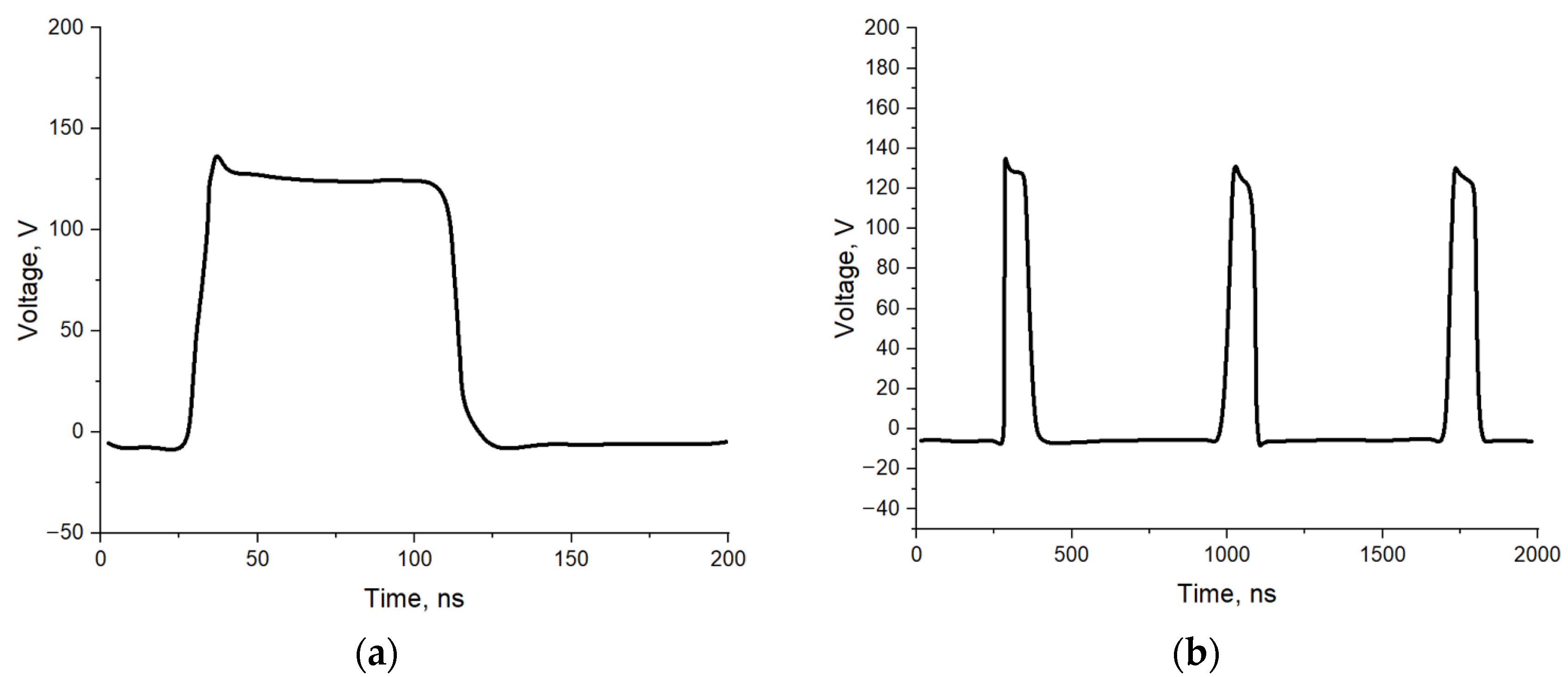
The measured waveforms are plotted in the
Figure 10. We were able to achieve 6.5 ns rise and 5.9 ns fall time with FSWP-51-02. We gradually ramped the supply voltage and the repetition rate and achieved pulse amplitude of 500 V (10 A at the load) and repetition rate of 1.4 MHz. At this point, we were too cautious and did not exceed 500 V peak voltage. We have also noticed that the switch temperature rose to 50 °C while operating the system at 500 V. This heating corresponds to high intrinsic resistance of the MOSFET (~55 Ω), which leads to a 50% loss in the transistor itself.
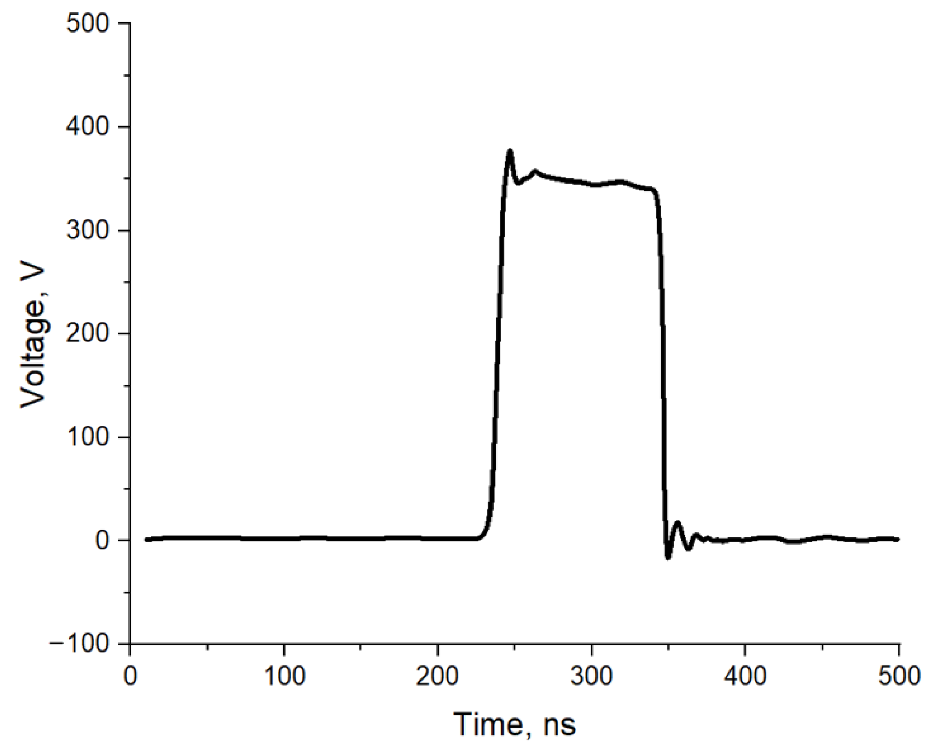
While in the process of deciding whether to purchase the second identical FSWP-51-02 switch for testing their combined output, Behkle announced a novel switch FSWP-51-06 based on GaN technology which has ~3 Ω intrinsic resistance and rated to 5.5 kV and 60 A. The main advantage of GaN-based switch as opposed to MOSFET version is in much lower intrinsic losses. We purchased and tested the GaN-based FSWP-51-06 on our HV test stand and successfully achieved 6.8 ns rise and 4.5 ns fall times with 1.5 ns jitter for 410 V/8.2 A pulses at 1.4 MHz PRF with 82% efficiency, as shown in
Figure 11. With such short rise/fall times demonstrated, there is solid basis to expect the GaN-based switch to work on an electron bunching frequency up to 88 MHz.
The next step is to gradually increase the input DC level in order to achieve our goal 1.1 kV/22 A at the output. As GaN performance is dependent on the transmitted power level itself, further testing will be done with a DC supply capable of providing up to 2 kV and 40 A. This exceeds the power for the current application, but slow ramping of its output will experimentally define the requirements on the actual DC source that will be used in the final pulser prototype.
5. Discussion and Conclusions
An ion-clearing gap for an electron cooling system is required to operate the next generation of ultra-high luminosity nuclear physics colliders such as the EIC lepton-hadron collider. In this paper, we presented a HV kicker design, capable of achieving an 20 mrad deflecting angle of 7 MeV electron bunch. Based on the optimization of several kicker parameters, we found that its effective length should be 40–50 cm, and the required peak voltage is 1200 V. We showed that solid-state HV switches are capable of providing 92 ns-long pulses at 1.4 MHz rep rate with 10 ns rise/fall times.
In addition to being an enabling technology for EIC, the proposed system or its constituent blocks may find various uses in HV switching applications, including fast beam choppers [
17] for injector test facilities, the next-generation free electron laser (FEL) light sources [
18], and inverse Compton scattering gamma ray sources using ERLs [
19], ion-clearing gaps for ion accelerators, as well as inverse FEL-driven replacement of radio frequency quadrupole (RFQ) accelerating structures [
20].
Industrial and defense applications include multi-kW drivers of Pockels cells for high average power lasers, heat management of high-power Class-F [
21] microwave solid state power GaN amplifiers [
22], high-power DC–DC and AC–DC convertors, directed energy broadband systems, geo-radars employed in geophysics, and high-power military electronics.


 ,
, 


