Article

Thermo-Optic Phase Tuners Analysis and Design for Process Modules on a Silicon Nitride Platform

1
Photonic ICgroup at the Photonics Research Labs, Universitat Politècnica de València, C/Camino de Vera s/n, 46022 València, Spain
2
Instituto de Microelectrònica de Barcelona (IMB-CNM, CSIC), C/del Til·lers. Campus, Universitat Autònoma de Barcelona (UAB), 08193 Cerdanyola del Vallès, Spain
*
Author to whom correspondence should be addressed.
Photonics 2021, 8(11), 496; https://doi.org/10.3390/photonics8110496
Submission received: 1 October 2021 / Revised: 3 November 2021 / Accepted: 3 November 2021 / Published: 5 November 2021

Abstract

:
In this paper, we present a systematic design for manufacturing analysis for thermo-optic phase tuners, framed within the process modules available on a silicon nitride platform. Departing from an established technology platform, the heat distribution in various micro-structures was analyzed, both in steady and transient states, employing a 2D heat transfer model solved numerically. Multi-parametric simulations were performed on designs combining trenches and substrate undercut, by varying their position and dimensions. The simulation results were compared to a reference conventional fully-clad cross-section. Deep air-filled trenches are shown to reduce the power consumption up to 70%, alongside a thermal crosstalk phase shift reduction of more than one order of magnitude (0.045 π rad/mm), at the expense of a slightly lower bandwidth (11.8 kHz). The design with trenches and substrate undercut lowers the power consumption up to 97%, decreases two orders of magnitude the crosstalk (0.006 π rad/mm), at the cost of less than one order of magnitude in bandwidth (0.9 kHz). In the works, we selected three different heater materials (Cr/Au, Al, poly-silicon) offered by the fab and four different heater widths (2.5 to 7 μ m). Their combinations are related to performance, reliability and durability of the devices, strongly linked to temperature, current density, and Omegaic resistance. The different figures of merit defined, and the methodology followed, can be mimicked by future designers to take design decisions at bird’s eye.

1. Introduction

The high demand for discrete optical devices in many applications over the four last decades, fostered a rapid evolution and cost reduction in the photonics subsystems. With photonics becoming ubiquitous in many application domains, there is a general demand for the reduction in space, weight, and power (SWaP) consumption. During the last two decades, the generic technology philosophy and the multi-project wafer (MPW) runs [1,2] allowed a step forward on photonic integrated circuits (PICs) technologies, due to the development of new fabrication processes for different technology platforms. These have paved the way for an effective integration, reducing manufacturing costs, and SWaP requirements while increasing performance and stability. The three main established photonic technologies [3,4,5,6] are based on Silicon (Si), Indium Phosphide (InP) [7,8,9], and Silicon Nitride (SiN) [10,11,12] with differentiated performances depending on the device function: III–V semiconductors for light generation, amplification and modulation, Si Photonics for detection and modulation and SiN for broadband applications ranging from visible to mid-infrared.
To perform more and more advanced complex optical functions, PICs are sought to have a high level of reconfiguration, which up to a large extent is served by manipulating the phase of the electro-magnetic field. Thus, optical phase shifters are key components for the realization of subsystems, such as antenna beam-formers in wireless communications [13,14], optical phased arrays in Light Detection and Ranging (LIDAR) systems [15,16], optical signal processors [17], microwave photonics circuits [14,18], and switches in optical communications [19,20,21,22], among others. An optical phase shift can be achieved through three different mechanisms: electro-refraction, electro-absorption, and the thermo-optic (TO) effect. The two first are mainly used in modulators and are based on an electric field applied directly through the material, where the optical signal propagates, resulting into faster, less power consuming phase shifters. However, in some cases, such as in Si due to the free carrier absorption effect, they induce optical losses. On the other hand, the thermo-optic effect acts directly over the real part of the refractive index, induces less optical loss, but at the cost of power and bandwidth.
Nonetheless, thermal tuners can be engineered for small footprint and modest power consumption, while having kHz bandwidth, which is sufficient for many reconfigurable PIC applications. Integrated thermo-optic phase shifters have been reported in the literature for different purposes, such as: wavelength [23] and mode [24] (de)multiplexing in WDM and SDM networks, respectively, switching applications [19,20,21,22], optical phase arrays for antenna beam forming networks (OBFN) in wireless communications [15] and for optical beam steering in LIDAR applications [13,15,16,25], microwave signal processing [14,18], among others. In some applications of PICs, compactness is key in terms of functionality per unit area, such as in [26] or in [17,27]. Therein the authors demonstrated programmable photonic processors implemented by a two-dimensional photonic waveguide mesh using two different types of tunable basic units: Mach Zehnder Interferometers and directional couplers. Each side of the mesh elements contains two parallel TO phase shifters. In this application, the miniaturization of the TO phase shifter would allow a higher number of mesh cells and, thus, more advanced functions in the same chip area. Despite some approaches in literature proposing the use of long and wide tuners for linear phase shift [14,23] over driving power, this is contrary to the spirit of integrated circuits, where the chip area determines most of the device cost.
Power consumption and thermal crosstalk are the main drawbacks of integrated TO phase shifters, but resorting to some additional fab steps, techniques, or structures in order to overcome them have been demonstrated, including: the thermal isolation of the TO phase shifter by means of trenches and undercuts [28,29,30,31,32], the heat flux transfer increase towards the shifter’s waveguide by inserting high thermal conductivity materials [33] or dopants at specific locations of the shifter [32]. In the present work, we show a design for manufacturability flow addressing the thermal wanted and unwanted effects, by analyzing how the dimensions and position of known micro-structures, such as trenches and undercuts, besides the heater material, are related to the performance parameters: power consumption, cross-talk, and bandwidth. A discussion on durability and the inter-relation of all the figures of merit (FoM), including footprint, closes the paper.

2. Thermo-Optic Phase Shifter Working Principle

In the following we summarize the fundamental equations needed in this work, that describe the TO phase shift mechanism, and can be found elsewhere [34]. For a TO shifter, the optical phase change related to a temperature change altering the effective refractive index of the waveguide, is given by:
Δ Φ / 2 π = 1 λ Δ n e f f w g L = 1 λ n e f f w g T Δ T w g L
where λ is the wavelength, n e f f w g / T is the TO coefficient that affects the effective refractive index, Δ T w g is the temperature increase in the waveguide (subscript ’wg’) and L is the length of the waveguide where Δ T w g is applied. The TO phase shifters use a Joule heat source in the shape of an electrical conductor. The Joule law states that an electrical current, I, through a resistor of resistance R h , produces heat power proportionally to the square of the current by the resistance of the conductor:
P = I 2 R h [ W ]
The heat energy generated by the collisions of the carriers with ions within the conductor, is mostly transferred due to the Fourier Law or heat conduction [34]. The Fourier law indicates that a heat flux Q exists for a temperature gradient in a solid or liquid medium:
Q = k d T d y = k T 1 T 2 y 1 y 2
where k [ W / m · K ] is the thermal conductivity of the material, T 2 and T 1 the temperatures at the points between the heat transfer takes place, y 2 and y 1 . As long as the separation decreases or the thermal conductivity of the material increases, the heat flux increases. This constitutes an important design consideration for a TO phase shifter, materials and dimensions. Additionally, the maximization of heat transfer to the optical waveguide, and hence, the reduction in heat losses, is key as well.

3. Heat Transfer Modeling

In order to investigate the heat transfer on integrated TO phase shifters, we considered the heat transfer equation [35]. Retaining only the conductive and neglecting the convective and radiative heat transfer modes, results into:
C p ρ d T d t + ( k T ) = Q
where C p [ J / k g · K ] is the specific heat capacity of the material, ρ is the material density [ k g / m 3 ] , dT/dt is the temperature change rate at the material over time, T is the temperature gradient and Q is the heat flux transfer [ W / m 3 ] . At steady state regime, there is no variation of temperature over time and Equation (4) results into Equation (5), where 2 T is the Laplace operator:
k 2 T = Q
In our simulations, Equations (4) and (5) are solved in MATLAB using the 2D finite element analysis PDE toolbox.

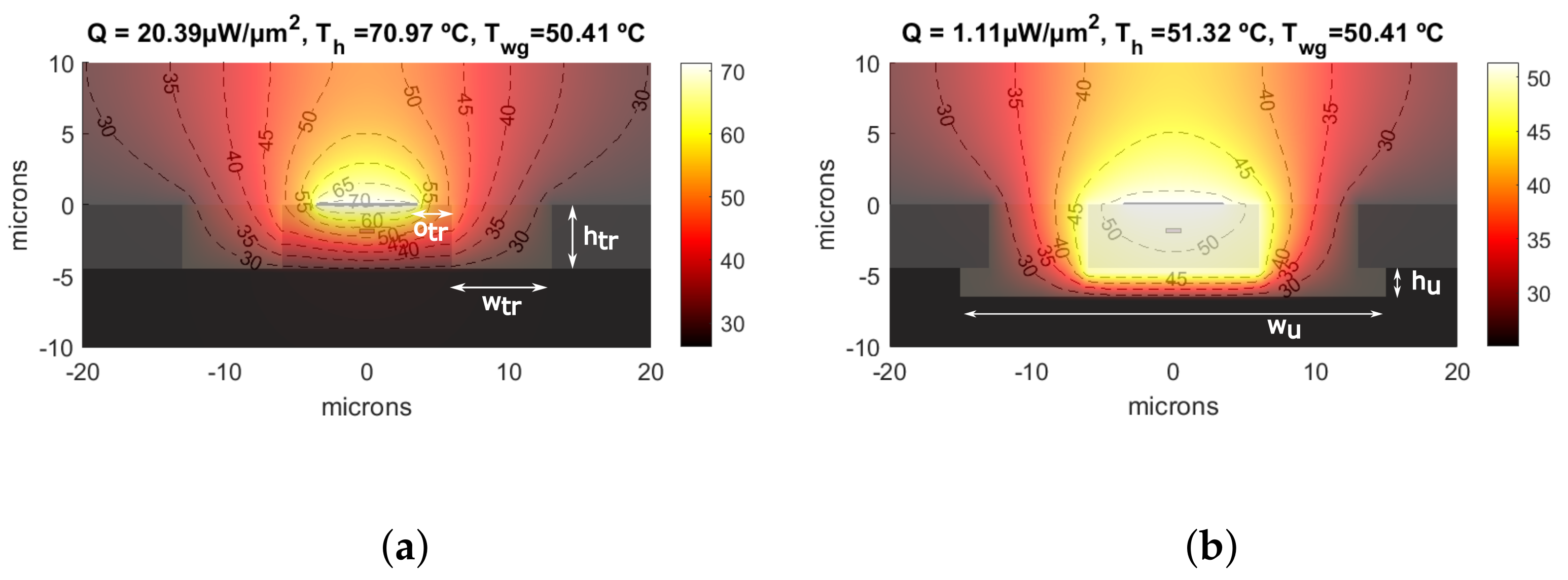
3.1. Reference Cross-Section

The reference cross-section analyzed corresponds to the SiO 2 fully-clad shifter that is shown in Figure 1a, with an optical SiN waveguide embedded in silica, and the heater on top, which matches the existing CNM-VLC SiN technology platform [36].
Hence, the simulation framework is set up to model the heat transfer of three different TO phase shifter cross-sections: fully-clad, air-trenched, and silicon undercut, including air-trenches. The first boundary condition is a fixed temperature at the bottom of the Si wafer, set to 25 °C, emulating a typical temperature controller. An internal heat source emulates the Joule heating coming from the micro-resistor. We set the framework to calculate the temperature distribution along the whole simulation window, as well as to extract the heater’s and waveguide’s temperature. Furthermore, in order to evaluate the cross-talk in the horizontal direction, the temperature profile at the waveguide depth along the whole simulation window is retrieved as well. The rise and fall time ( T r , T f ) are extracted from the transient state simulations as the required time to heat the waveguide 10–90% of the required waveguide temperature for a pi phase shift, and to cool down from 90% to 10%. The simulator considers the most restrictive time to calculate the BW as 0.35/( T r or T f ).
Prior to running multi-parametric simulations, several convergence tests were performed to determine the width and height of the simulation window, the mesh grid parameters and the simulation time, having as target a temperature variation smaller than 0.15%. The simulation window width and height were found to be 1.0 × 0.515 mm 2 . Next, the framework was used to reproduce our simulation and experimental results from [37], obtaining the same, but in the present work with a different simulation environment.
The cross section of the fully-clad TO phase shifter, considering the layer thicknesses and materials of the SiN CNM-VLC platform, are shown in Figure 1a. The parameters of the following simulations considered an optical phase shift of π ( Δ Φ π ) at 1550 nm optical wavelength, on a 1 μ m waveguide core width, along a 1 mm shifter length ( l h ), using a 7 μ m and 0.1 μ m heater width ( w h ) and height ( w h ), respectively. The heater material is Au. The physical parameters used in the simulations are shown in Table 1. According to Equation (1) and considering a SiN effective thermo-optic coefficient of 3.05 × 10 5 [37], the required temperature increase ( Δ T w g ) at the waveguide core is 25.41 °C hence the required absolute temperature ( T w g ) is 50.41 °C, for the aforementioned 25 °C boundary condition at the bottom of the wafer. Figure 1b represents the temperature distribution along the cross-section at Δ Φ π . As shown in the figure, a heat flux Q 0 = 22.82 μ W/ μ m 2 (note the units of heat flux are now for m 2 , due to the 2D modeling tool used) is required in the heater to increase the waveguide temperature to T w g and induce a Δ Φ π phase shift. For this, the required temperature in the heater is 71.75 °C.
Figure 1c shows the temperature profile at the waveguide’s depth along the horizontal direction. As expected, the temperature at the location of the waveguide is 50.41 °C. Further away, the temperature exceeding the reference value of 25 °C is considered as crosstalk on a hypothetical waveguide located next to the actual shifter under study. The undesired temperature increase in these locations induces an unwanted phase shift, shown in the right axis in Figure 1c. In addition to the previous steady state simulations, transient state results—for a temperature step in the heater—are reported in Figure 1d. The obtained rise time and associated BW are 26.43 μ s and 13.22 kHz, respectively.

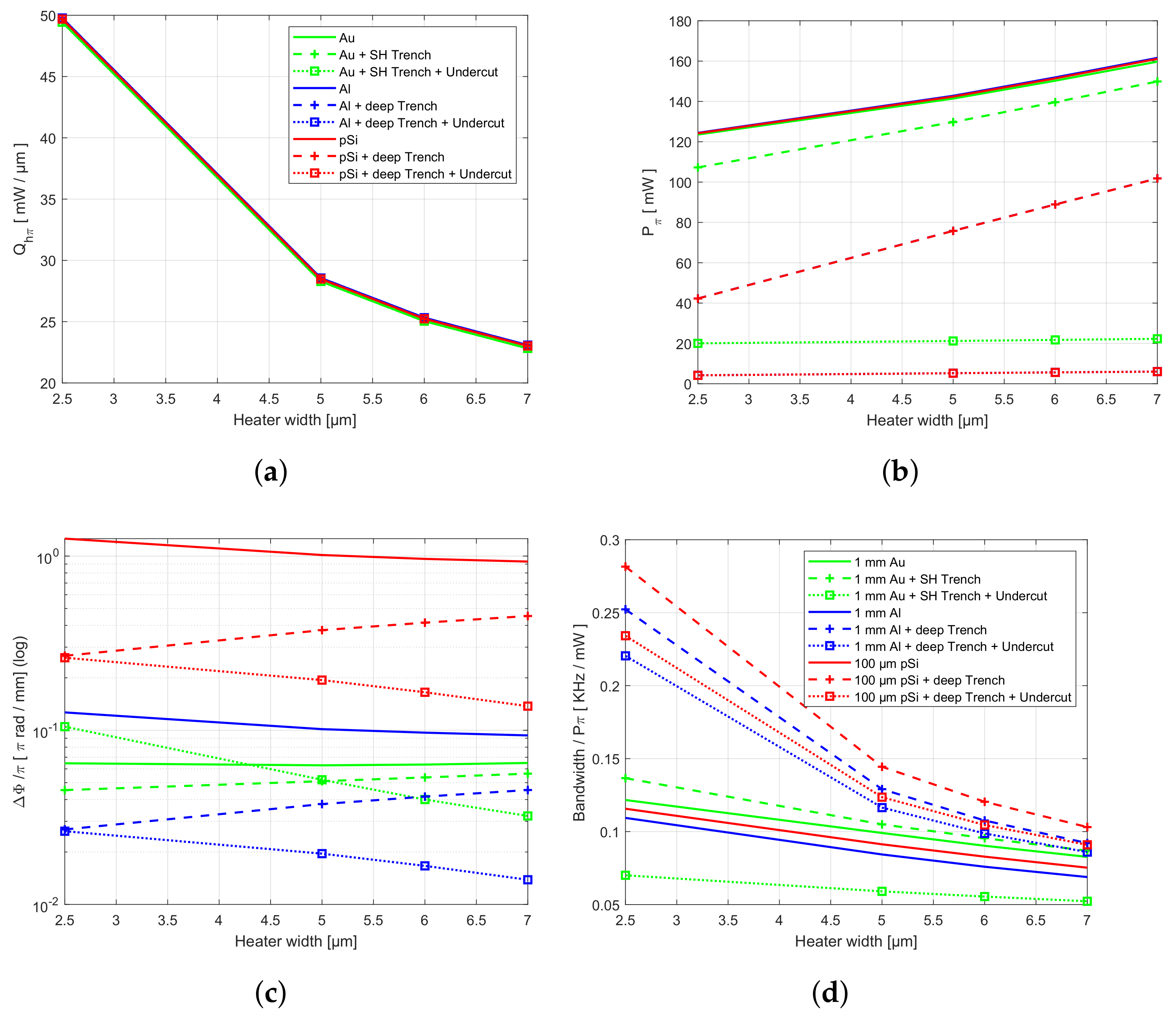
3.2. Multi-Parametric Analysis of Improved Cross-Sections

Departing from the reference cross-section, we proceed to improve the heat transfer from the heater to the waveguide by reducing the thermal resistance and losses. To do so, two types of structures were incorporated to the fully-clad TO phase shifter geometry: air-filled trenches and undercuts. In the design with trenches Figure 2a, the SiO 2 cladding is eliminated at both sides of the heater down to the silicon surface and filled with air. The design with undercut, in addition to the trenches, has a portion of silicon removed below the silica substrate [28,29,30,31,32], shown in Figure 2b.
In order to investigate the influence of the various dimensions on the TO shifter’s performance, these were parametrized, as illustrated in Figure 2: the trench width ( w t r ), the separation distance from the end of the heater to the start of the trench ( o t r ), the height of the trench ( h t r ), and the width and height for the undercut ( w u and h u , respectively). The temperature distributions, under the same phase shift conditions previously described, for both geometries, and a fixed set of the previously listed parameters, are shown in Figure 2. As expected, the design including trenches and undercut exhibits a much better thermal isolation, where the heat flux is minimized, and thus the heater temperature. Next, the multi-parametric runs for the different dimensions of both cross-sections were performed. At every iteration, a new shifter geometry was created considering a new dimensional value of the trench or the undercut, always keeping the same heater and layer properties.
From the framework, at every iteration, we obtain the required Q and heater temperature for a π phase shift, as previously. By comparing the required heat flux Q to produce the Δ T w g at every iteration with Q 0 , the heat flux reference corresponding to the fully-clad shifter, we define the consumption reduction (CR) figure of merit (FoM) of the new geometry as:
CR = ( 1 Q Q 0 ) * 100 [ % ]
The first set of simulations corresponds to the cross-section with air trenches. For fixed heater and trench widths (both set to 7 μ m), the trench height and offset were swept. The obtained CR is given as a contour plot in Figure 3a, showing it can be maximized by both lowering o t r and increasing h t r . However, the former has significantly more effect than the latter. Negative values of o t r indicate that the start of the trench is below the heater, being the heater partially suspended in air. We define now the crosstalk phase shift FoM as the undesired phase shift at a distance D x t from the center of the waveguide, given by:
D x t = ( 2 * w h / 2 ) + w t r + ( 2 * o t r ) for o t r > 0 , ( 2 * w h / 2 ) + w t r for o t r < 0
This distance corresponds to the nearest possible location of another identical TO phase shifter sharing the same trench, for a given o t r , w t r and w h . We recall w t r and w h are kept fixed to 7 μ m, thus only o t r is changing D x t for this first set of simulations. The crosstalk phase shift results are given in Figure 3b. Since the optical phase is accumulative, our metric is normalized per unit length. For h t r values below 1.5 μ m the trench offset has little impact on this FoM. For larger values the results are consistent with the CR plot of panel (a), i.e., when heat is kept at the target waveguide (CR high), there is less unwanted phase shift at D x t . From panel (b), for h t r = 4.5   μ m and o t r = 0.1   μ m the phase shift cross-talk is 0.045 [ π rad / mm ] , approximately half of that for the fully-clad shifter in Figure 1c, that is 0.094 [ π rad / mm ] at the same horizontal distance (14 μ m). Finally, using transient state simulations, the TO phase shifter BW is reported in Figure 3c. Compared to the reference cross-section, and the BW of 13.22 kHz derived from Figure 1d, for o t r < 1.5 μ m and h t r < 2.5 μ m a BW increase is observed. This boost can be attributed to the fact the trenched cross-section is more directional in terms of heat transfer, and hence heat reaches faster the waveguide core. For the same cross-section, now we fix the trench height to a value of 4.8 μ m, that corresponds to the existing process module used to etch away the SiO 2 waveguide cladding and BOX in the standard SiN CNM-VLC. The results are shown in the left column panels (a), (c), (e) of Figure 4. As general remarks, note all the results are strongly dependent on o t r . Both CR and crosstalk are improved for lower values of o t r , for the same reasons previously explained, directional heat transfer. Regarding the influence of w t r in CR, it shows in Figure 4a a flat response for values higher than 4µm and a weak deterioration for lower values. This is explained by the low thermal conductivity of the air-trench, which is laterally isolating the heat. On the other hand, the increase in the trench width shows an improvement of the phase shift crosstalk since the measured crosstalk point is further away than for narrower trenches.
A second set of simulations is incorporated, considering both trenches and undercut. The results are shown in the right column of Figure 4, panels (b), (d), and (f). These consist of sweeps of both the width and the height of the undercut, while the trench dimensions are kept fixed: w t r = 7 μ m, o t r = 2.5 μ m, h t r = 4.8 μ m. The heater dimensions are the same than in previous simulations: w h = 7 μ m, l h = 1 mm and h h =0.1 μ m. Once more, CR and crosstalk are linked, when CR is improved, crosstalk is reduced accordingly. Next, by roughly comparing the two columns in Figure 4, undercuts provide a two-fold improvement in CR and one order of magnitude improvement in crosstalk, at the cost of a BW reduction by a factor of ten. The height of the undercut does not affect significantly (only for undercut widths higher than 15 μ m). With respect to the bandwidth FoM, its link to the CR follows the same rationale as before, if heat is confined (for increasing undercut widths), the time required to be released is longer, hence the BW smaller.
In conclusion, the relations among the TO phase shifter FoMs power consumption, unwanted thermal crosstalk and bandwidth, have been set. In general, both power consumption and thermal crosstalk can be reduced, at the cost of operational speed. These improvements have been explored by simulation, but in the frame of the processes available in an actual SiN manufacturing platform, namely, selective area trenching and undercuts. At the starting discussion we highlighted the need for reconfiguration on PICs, with more and more basic units being crammed on a chip. Upon this perspective, the aspect of power consumption and its implications have been clarified. Nonetheless, we have not addressed yet the issue of device footprint. In all the simulation sets presented, we assumed a typical SiN heater length of 1 mm. Hence, the question pending to address is which are the limiting factors to miniaturize the TO shifter. Recall from Equation (1) that shortening the heater length implies a higher temperature increment Δ T w g to achieve the same phase shift, while the power consumption stays the same. The concentration of energy in smaller areas is connected to choice of heating element material through its properties, as elaborated in the following section.

4. Heating Element Design

Following the same philosophy, we frame our study to some of the available technologies of the SiN CNM foundry, that can be used to fabricate on-chip heating elements. These technologies pose restrictions on the heating element materials, dimensions, and floor-planning (relative dimensions) when combined with the surrounding materials (e.g., SiO 2 ) and processes (trench and undercut lithography and etch). Consequently, three sets of heating element designs are explored, amenable for fabrication in the CNM fab.
The first heater material considered is the standard bi-layer offered within the current SiN CNM-VLC platform, as in the previous section. The bi-layer is fabricated by sequential evaporation of chromium (Cr) and gold (Au), with thicknesses of 10 nm and 90 nm, respectively. This was already pictured in Figure 1a. Experimentally, the bi-layer sheet resistance was found to be 0.368 Ω / sq [37]. The lift-off process employed to pattern the heater requires a clearance offset o t r = 2.5 μ m to the trenches. Additionally, the etch depth for the trenches is limited in the current process flow to 2.3 μ m, which is the thickness of the silica cladding, Figure 1a.
The second heating material to consider is aluminum with 0.4% of copper, having a sheet resistance of 0.034 Ω / sq . In this case, it can be patterned by reactive ion etching (RIE). This allows o t r to be close to zero, and to create deeper trenches (4.8 μ m) down to the Si, Figure 1a.
As previously mentioned, shorter tuners require a higher Δ T w g , however the required heat energy is the same than for longer tuners although more concentrated. Hence, the heat flux is higher. The heating element resistance depends linearly with the length, according to:
R = ρ t h l h w h [ Ω ]
with ρ the resistivity of the material [ Ω · m ] and l h , w h and t h , the length, width, and thickness, respectively, of the heating line. Although, from a footprint perspective, a short length is preferred, a too short heater will have low resistance. Therefore more electrical current will be needed for a given required heat power, according to Joule’s law. When the electric current density flowing through the heating line is above a threshold, electro-migration takes place [38]. It consists on mass transport due to the momentum created by the collisions of electrons against metal atoms. In addition, the diffusion of the material is increased when the temperature is high [39], reducing the heater reliability. Therefore, relatively high resistivity materials should be considered to minimize current density.
Thus, the choice of the third material aims to meet compactness and resilience requirements. Poly-crystalline silicon (poly-Si) has been widely used in microelectronics industry for its excellent deposition quality, doping controlled resistivity and thermal properties [40,41,42]. For our designs, we have considered a 0.48 μ m thick poly-Si recipe from CNM, showing a sheet resistance of 16 Ω / sq . As in the aluminium case, the poly-Si is dry etched for patterning, and the trenches can be located at zero offset from the edge of the heater.
Since both Cr/Au and Al are of similar nature, the heating line length for these designs is 1 mm, owing to past experience [37]. Both require a Δ T w g of 25.41 °C for a Δ Φ π . For the poly-Si heater the length is pushed down to 100 μ m, for which Δ T w g = 254.1 °C. Table 2 compiles the dimensions of the heater, the air-trenches and silicon undercut for the three aforementioned heater materials. The physical and electrical properties considered in the simulations are listed in Table 1.
The simulation results are shown in Figure 5. These include a combination of each heater material, with the cross-sections investigated so far, namely fully-clad, with air-trenches and air-trenches combined with undercut. The heat flux per unit length required for an optical phase shift of π , Q h π , is shown in panel (a) for different heater widths. Reducing the heater width requires higher flux, since the same amount of energy needs to be delivered across a smaller surface.
From the heat flux, the power consumption to shift π , P π , can be calculated as follows:
P π = Q h π * w h * l h
The results are shown within Figure 5b. The required P π for the fully-clad designs is almost the same for the three heater materials since their thermal conductivity is almost two orders of magnitude higher than that of the SiO 2 cladding. Therefore, the limiting factor setting P π is the thermal resistance of SiO 2 . P π decreases for narrower heaters, since they concentrate heat and less is lost in its transfer down to the waveguide. The designs with trenches reduce P π from 160 mW to 100 mW for w h = 7 μ m aluminium and poly-Si heaters, and from 125 mW to 40 mW for w h = 2.5 μ m widths. In the gold heater case, the power reduction is lower since its trench is shallower (this difference is indicated in caption of Figure 5b as ‘SH’ vs. ‘DEEP’). The designs with undercut improve the P π down to 6 mW and 4 mW for widths of 7 and 2.5 μ m, respectively.
In Figure 5c, the thermal crosstalk phase shift per heater unit length results on an identical dummy TO shifter with same dimensions at D x t , Equation (7), are represented. Note that the cross-talk is given normalized to the heater length. Thus, the Al and poly-Si curves are exactly the same with a factor 10 corresponding to their length ratio (1 mm vs. 100 μ m). However, note that both the Al and poly-Si differ from the Au case for all cross-sections. This is due to two reasons. The main reason is that, through Equation (7) the cross-talk measurement point ( D x t ) is located where, from a manufacturable point of view, could be located an identical TO phase shifter, given the required technology to process the material. In the case of fully-clad designs, the D x t is also considered as it had trenches, in order to properly compare its results with designs with trenches or undercut, given a heater material. Thus, in the Au case which has an o t r of 2.5 μ m, the D x t is 4.8 μ m further away than the Al and poly-Si cases, hence the cross-talk is lower. The second reason is that, in the trench and undercut cases, the Al and poly-Si have the same lateral cross-section, that is, SiO 2 fully etched down to the Si, whereas de Au case has the SiO 2 only removed partially (just the cladding, but not the substrate). This means that the lateral resistance of the Al and poly-Si cases is the same, but different to the Au case. Despite they are not represented in the Figure 5c, for the sake of clarity, additional simulations confirmed that the Au case is exactly equivalent to the other two with o t r = 0.1 μ m. We did also check the heater height has no influence, by performing an Au simulation with height 0.6 μ m.
This said, for the fully-clad cases (all three have the same lateral thermal resistance, all the SiO 2 present) increasing the heater width, results in an increased D x t , that means smaller cross-talk (dummy point further away). However, when only trenches are used, the cross-talk increases with w h ( D x t ), which seems contrary to what expected. The reason is narrower w h the heat is directed better downwards, and the exponential decay of temperature from the waveguide core, happens faster in a narrower area. This can be said otherwise: there is less heat wasted laterally in narrow heater configurations.
In Figure 5c, we observe the Au based heater using trenches and undercut exhibits larger thermal crosstalk than the fully-clad or just trenched cross-section. Despite being somehow artificial (it would be tricky to make undercuts without deep trenches), we present it because it is an evidence of lateral heat tunneling along the silica layer. Said otherwise, the undercut prevents heat to flow down to the silicon, but in this case the silica is not fully etched, and, therefore, the heat flows along this low thermal resistance path (lateral). That explains why the cross-talk is higher for the case with both trenches and undercut, than for the fully-clad or just trenched cross-section.
Last but not least, we introduce a new FoM which to our understanding is relevant, the bandwidth available per unit power to shift π , BW/ P π . From the previous discussions, we found that isolation of the TO shifter area results into increased power efficiency, at the cost of BW. Hence, the proposed ratio represents a balance of both. The results for the different technologies analyzed are plotted in Figure 5d. For each heater line material, the best ratio is obtained for trenched TO shifters. For example, the poly-Si trenched heater of width w h = 5 μ m has a ratio of approximately 0.145 kHz/mW, and P π = 75 mW (BW = 10.875 kHz). The same, with undercuts shows 0.125 kHz/mW, that yields BW = 0.625 kHz ( P π = 5 mW).
If we now go back to the crosstalk phase shift, we observe values of 0.39 and 0.2 π rad/mm for these two configurations, respectively. Hence, it could be roughly stated the integration density is x2 for the undercut heaters, with power saving of x15, but at a cost of approximately x17 in BW. This could be a point in which economics should be considered, so as to evaluate the application specifications vs. integration density vs. fabrication complexity costs. However, this is out of the scope of this paper. In conclusion, by inspecting jointly plots as the ones shown in panels (b), (c), and (d) of Figure 5, the designer has information to judge at bird’s eye which is the best TO shifter design for a given PIC application. Nonetheless, there is an additional aspect to cover, with respect to the maximum temperature a heater line of a given material can withstand.
Hence, we next give some insight into the factors that degrade heaters reliability and durability, temperature, and current density. In Figure 6a we present the heater line temperature required for an optical phase shift of π , termed T h π . Although the 1 mm heaters have T h π in the range of 71 to 85 °C, the 100 μ m length poly-Si heater reaches temperatures as high as 620 °C for the 2.5 μ m width fully-clad design down to 482 and 294 °C for the trenched design and undercut one, respectively. These, in turn, are extremely high temperatures used in, e.g., ignition applications in solid propellant microthrusters [43]. Complementarily, we show in Figure 6b the corresponding required current density J h π . The values are quite differentiated depending on the heater material due to the dissimilar resistance obtained. The values for the poly-Si, which is the most resistive are 1, 0.6, and 0.16 MA/cm 2 for the fully-clad, trenched, and undercut configurations, respectively. These values are well below the reverse annealing point (1.5 MA/cm 2 ), transition point (3 MA/cm 2 ) and breakdown point (6 MA/cm 2 ) reported in [44] for a similar poly-Si resistor. Note, however, these limits depend on structural properties of the material (grain size), that are particular to each fabrication process. In the presented designs, the 100 μ m heater is an extreme case requiring high T h π , but from the material durability point of view this seems feasible. On the contrary, while the T h π is modest for the Au and Al based heaters, the associated current density for an optical shift of π is above the mentioned limits, and thus electro-migration could take place. On the other hand, some applications may not require reaching a π phase change, and, therefore, the required temperature and associated current density are lower.

5. Conclusions and Outlook

In this paper we have addressed the topic of thermo-optic heater design from a design-for-manufacturability perspective. Departing from an established PIC integration process, and considering actual available materials and fabrication processes, sets of micro-structures have been analyzed using multi-parametric simulations. The relevant figures of merit have been defined and their relations established, in summary, the heat flux and electric power consumption, the thermal crosstalk and the operational bandwidth.
From the heat conductivity point of view, due to the thermal resistance lowering, air trenches and silicon undercut reduce power consumption and thermal crosstalk, at the cost of operational speed. Reducing the heater width results into increased efficiency, since the heat is more focused. The TO shifter’s performance has been linked to two key operational aspects, which are reliability and durability. From this point of view, the length is a critical parameter since it determines the required temperature increase in the waveguide, and the choice of the heater material, also proves crucial. A higher resistive material requires less current and thus, less current density. Both required temperature increase and current density are the factors that degrade reliability and durability. By following a similar flow with these figures of merit, a designer can have a framework in which to trade-off application specifications to manufacturable designs.

Author Contributions

R.A., P.M. and D.P. developed the heat transfer model. R.A., P.M. and C.D. defined the phase shifter’s cross sections. R.A. and P.M. programmed the simulator. C.D. provided information regarding to fabrication concerns. R.A. performed the simulations and wrote the paper with the support of all the co-authors. All authors have read and agreed to the published version of the manuscript.

Funding

This research was funded by Ministry of Economy, Industry and Competitiveness grants numbers TEC2016-80385-P SINXPECT and PID2019-110877GB-I00 BHYSINPICS, Generalitat Valenciana grant number PROMETEO/2017/103, Ministry of Science, Innovation and Universities grant number MCIU-RTI2018-100773-B-C31 and by H2020 Marie Sklodowska Curie Innovative Training Network grant number MICROCOMB (GA 812818).

Data Availability Statement

The data presented in this study are available within the article.

Conflicts of Interest

The authors declare no conflict of interest.

References

  1. Muñoz, P. Photonic integration in the palm of your hand: Generic technology and multi-project wafers, technical roadblocks, challenges and evolution. In Proceedings of the 2017 Optical Fiber Communications Conference and Exhibition (OFC), Los Angeles, CA, USA, 19–23 March 2017; pp. 1–3. [Google Scholar]
  2. Muñoz, P. Photonic integrated circuits using generic technologies. IEEE Photonics Soc. Newsl. 2016, 30, 4–12. [Google Scholar]
  3. Bogaerts, W.; Baets, R.; Dumon, P.; Wiaux, V.; Beckx, S.; Taillaert, D.; Luyssaert, B.; Campenhout, J.V.; Bienstman, P.; Thourhout, D.V. Nanophotonic waveguides in silicon-on-insulator fabricated with CMOS technology. J. Light. Technol. 2005, 23, 401–412. [Google Scholar] [CrossRef]
  4. Ambrosius, H.P.M.M.; Leijtens, X.J.M.; de Vries, T.; Bolk, J.; Smalbrugge, E.; Smit, M.K. A Generic InP-based Photonic Integration Technology. In Proceedings of the IPRM 2011—23rd International Conference on Indium Phosphide and Related Materials, Berlin, Germany, 22–26 May 2011; pp. 1–4. [Google Scholar]
  5. Leinse, A.; Heideman, R.G.; Klein, E.J.; Dekker, R.; Roeloffzen, C.G.H.; Marpaung, D.A.I. TriPleX platform technology for photonic integration: Applications from UV through NIR to IR. In Proceedings of the 2011 ICO International Conference on Information Photonics, Ottawa, ON, Canada, 18–20 May 2011; pp. 1–2. [Google Scholar] [CrossRef]
  6. Aalto, T.; Cherchi, M.; Harjanne, M.; Sun, F.; Kapulainen, M. 3-micron Silicon Photonics. In Optical Fiber Communication Conference; Optical Society of America: San Diego, CA, USA, 2018. [Google Scholar] [CrossRef]
  7. Smit, M.; Leijtens, X.; Ambrosius, H.; Bente, E.; Van der Tol, J.; Smalbrugge, B.; De Vries, T.; Geluk, E.J.; Bolk, J.; Van Veldhoven, R.; et al. An introduction to InP-based generic integration technology. Semicond. Sci. Technol. 2014, 29, 083001. [Google Scholar] [CrossRef]
  8. Augustin, L.M.; Santos, R.; den Haan, E.; Kleijn, S.; Thijs, P.J.; Latkowski, S.; Zhao, D.; Yao, W.; Bolk, J.; Ambrosius, H.; et al. InP-based generic foundry platform for photonic integrated circuits. IEEE J. Sel. Top. Quantum Electron. 2017, 24, 1–10. [Google Scholar] [CrossRef]
  9. Soares, F.M.; Baier, M.; Gaertner, T.; Feyer, M.; Möhrle, M.; Grote, N.; Schell, M. High-performance InP PIC technology development based on a generic photonic integration foundry. In Optical Fiber Communication Conference; Optical Society of America: San Diego, CA, USA, 2018; p. M3F–3. [Google Scholar]
  10. Muñoz, P.; Micó, G.; Bru, L.A.; Pastor, D.; Pérez, D.; Doménech, J.D.; Fernández, J.; Baños, R.; Gargallo, B.; Alemany, R.; et al. Silicon Nitride Photonic Integration Platforms for Visible, Near-Infrared and Mid-Infrared Applications. Sensors 2017, 17, 2088. [Google Scholar] [CrossRef]
  11. Blumenthal, D.J.; Heideman, R.; Geuzebroek, D.; Leinse, A.; Roeloffzen, C. Silicon Nitride in Silicon Photonics. Proc. IEEE 2018, 106, 2209–2231. [Google Scholar] [CrossRef] [Green Version]
  12. Munoz, P.; van Dijk, P.W.; Geuzebroek, D.; Geiselmann, M.; Dominguez, C.; Stassen, A.; Doménech, J.D.; Zervas, M.; Leinse, A.; Roeloffzen, C.G.; et al. Foundry developments toward silicon nitride photonics from visible to the mid-infrared. IEEE J. Sel. Top. Quantum Electron. 2019, 25, 1–13. [Google Scholar] [CrossRef]
  13. Sun, J.; Timurdogan, E.; Yaacobi, A.; Hosseini, E.S.; Watts, M.R. Large-scale nanophotonic phased array. Nature 2013, 493, 195–199. [Google Scholar] [CrossRef]
  14. Roeloffzen, C.G.; Zhuang, L.; Taddei, C.; Leinse, A.; Heideman, R.G.; van Dijk, P.W.; Oldenbeuving, R.M.; Marpaung, D.A.; Burla, M.; Boller, K.J. Silicon nitride microwave photonics circuits. Appl. Phys. Lett. 2013, 21, 22937–22961. [Google Scholar] [CrossRef] [Green Version]
  15. Kwong, D.; Hosseini, A.; Covey, J.; Zhang, Y.; Xu, X.; Subbaraman, H.; Chen, R.T. On-chip silicon optical phased array for two-dimensional beam steering. Opt. Lett. 2014, 39, 941–944. [Google Scholar] [CrossRef] [Green Version]
  16. Wang, Y.; Liang, L.; Chen, Y.; Jia, P.; Qin, L.; Liu, Y.; Ning, Y.; Wang, L. Improved performance of optical phased arrays assisted by transparent graphene nanoheaters and air trenches. RSC Adv. 2018, 8, 8442–8449. [Google Scholar]
  17. Pérez, D.; Gasulla, I.; Crudgington, L.; Thomson, D.J.; Khokhar, A.Z.; Li, K.; Cao, W.; Mashanovich, G.Z.; Capmany, J. Multipurpose silicon photonics signal processor core. Nat. Commun. 2017, 8, 636. [Google Scholar] [CrossRef] [PubMed] [Green Version]
  18. Fandiño, J.S.; Muñoz, P.; Doménech, D.; Capmany, J. A monolithic integrated photonic microwave filter. Nat. Photonics 2016, 11, 124–130. [Google Scholar] [CrossRef] [Green Version]
  19. Zheng, D.; Doménech, J.D.; Pan, W.; Zou, X.; Yan, L.; Pérez, D. Low-loss broadband 5× 5 non-blocking Si3N4 optical switch matrix. Opt. Lett. 2019, 44, 2629–2632. [Google Scholar] [CrossRef]
  20. Fang, Q.; Song, J.F.; Liow, T.Y.; Cai, H.; Yu, M.B.; Lo, G.Q.; Kwong, D.L. Ultralow Power Silicon Photonics Thermo-Optic Switch With Suspended Phase Arms. IEEE Photonics Technol. Lett. 2011, 23, 525–527. [Google Scholar] [CrossRef]
  21. Fang, J.S.Q.; Tao, S.H.; Liow, T.Y.; Yu, M.B.; Lo, G.Q.; Kwong, D.L. Fast and low power Michelson interferometer thermo-optical switch on SOI. Opt. Express 2008, 16, 525–527. [Google Scholar]
  22. Watts, M.R.; Sun, J.; DeRose, C.; Trotter, D.C.; Young, R.W.; Nielson, G.N. Adiabatic thermo-optic Mach–Zehnder switch. Opt. Lett. 2013, 38, 733–735. [Google Scholar] [CrossRef] [PubMed]
  23. Hai, M.S.; Leinse, A.; Veenstra, T.; Liboiron-Ladouceur, O. A Thermally Tunable 1 × 4 Channel Wavelength Demultiplexer Designed on a Low-Loss Si3N4 Waveguide Platform. Photonics 2015, 27, 1065–1080. [Google Scholar]
  24. Melati, D.; Alippi, A.; Melloni, A. Reconfigurable photonic integrated mode (de)multiplexer for SDM fiber transmission. Opt. Express 2016, 24, 12625–12634. [Google Scholar] [CrossRef] [Green Version]
  25. Yaacobi, A.; Sun, J.; Moresco, M.; Leake, G.; Coolbaugh, D.; Watts, M.R. Integrated phased array for wide-angle beam steering. Opt. Lett. 2014, 39, 4575–4578. [Google Scholar] [CrossRef] [Green Version]
  26. Zhuang, L.; Roeloffzen, C.G.H.; Hoekman, M.; Boller, K.J.; Lowery, A.J. Programmable photonic signal processor chip for radiofrequency applications. Optica 2015, 2, 854–859. [Google Scholar] [CrossRef] [Green Version]
  27. López, D.P.; Gutierre, A.M.; Sánchez, E.; Dasmahapatra, P.; Capmany, J. Integrated photonic tunable basic units using dual-drive directional couplers. Opt. Express 2019, 27, 38071–38086. [Google Scholar] [CrossRef] [Green Version]
  28. Gilardi, G.; Weiming, Y.; Haghighi, H.R.; Leiijtens, X.J.M.; Smit, M.K.; Wale, M.J. Deept Trenches for Thermal Crosstalk Reduction in InP-Based Photonic Integrated Circuits’. J. Light. Technol. 2014, 32, 4864–4870. [Google Scholar] [CrossRef] [Green Version]
  29. Wu, X.; Liu, W.; Yuan, Z.; Liang, X.; Chen, H.; Xu, X.; Tang, F. Low Power Consumption VOA Array With Air Trenches and Curved Waveguide. IEEE Photonics J. 2018, 10, 501–503. [Google Scholar] [CrossRef]
  30. Malik, A.; Dwivedi, S.; Van Landschoot, L.; Muneeb, M.; Shimura, Y.; Lepage, G.; Van Campenhout, J.; Vanherle, W.; Van Opstal, T.; Loo, R.; et al. Ge-on-Si and Ge-on-SOI thermo-optic phase shifters for the mid-infrared. Opt. Express 2014, 22, 28479–28488. [Google Scholar] [CrossRef] [PubMed]
  31. Ceccarelli, F.; Atzeni, S.; Pentangelo, C.; Pellegatta, F.; Crespi, A.; Osellame, R. Low power reconfigurability and reduced crosstalk in integrated photonic circuits fabricated by femtosecond laser micromachining. arXiv 2020, arXiv:2001.08144. [Google Scholar] [CrossRef]
  32. Masood, A.; Pantouvaki, M.; Lepage, G.; Verheyen, P.; Van Campenhout, J.; Absil, P.; Van Thourhout, D.; Bogaerts, W. Comparison of heater architectures for thermal control of silicon photonic circuits. In Proceedings of the 10th International Conference on Group IV Photonics, Seoul, Korea, 28–30 August 2013; pp. 83–84. [Google Scholar]
  33. Zhu, S.; Hu, T.; Xu, Z.; Dong, Q.Z.Y.; Li, Y.; Singh, N. An improved Thermo-Optic Phase Shifter with AlN Block for Silicon Photonics. In Optical Fiber Communication Conference; Optical Society of America: San Diego, CA, USA, 2019; Volume 34, pp. 6898–6910. [Google Scholar]
  34. Bergman, T.L.; Incropera, F.P.; DeWitt, D.P.; Lavine, A.S. Fundamentals of Heat and Mass Transfer; John Wiley & Sons: Jefferson City, MO, USA, 2011. [Google Scholar]
  35. Murata, S.; Nakada, H.; Abe, T. Theoretical and experimental evaluation of the effect of adding a heat-bypass structure to a laser diode array. Jpn. J. Appl. Phys. 1993, 32, 1112. [Google Scholar] [CrossRef]
  36. VLC Photonics and Centro Nacional de Microelectrónica (CNM-VLC). Silicon Nitride Photonic Integration Platform. Available online: http://www.imb-cnm.csic.es/index.php/en/clean-room/silicon-nitride-technology (accessed on 14 April 2020).
  37. Pérez, D.; Baños, R.; Doménech, J.D.; Sánchez, A.M.; Cirera, J.M.; Mas, R.; Sánchez, J.; Durán, S.; Pardo, E.; Domínguez, C.; et al. Thermal tuners on a silicon nitride platform. arXiv 2016, arXiv:1604.02958. [Google Scholar]
  38. Lienig, J. Introduction to electromigration-aware physical design. In Proceedings of the 2006 International Symposium on Physical Design, San Jose, CA, USA, 9–12 April 2006; pp. 39–46. [Google Scholar]
  39. Lloyd, J. Electromigration for Designers: An Introduction for the Non-Specialist. Available online: https://www.eetimes.com/electromigration-for-designers-an-introduction-for-the-non-specialist/ (accessed on 14 April 2020).
  40. Gardes, F.Y.; Reed, G.T.; Emerson, N. A sub-micron depletion-type photonic modulator in Silicon On Insulator. Opt. Express 2005, 13, 8845–8854. [Google Scholar] [CrossRef]
  41. Lim, H.; Yin, H.; Xianyu, W.; Kwon, J.Y.; Zhang, X.; Cho, H.S.; Kim, J.M.; Park, K.B.; Kim, D.Y.; Jung, J.S.; et al. Ultra low sheet resistance on poly silicon film by Excimer laser activation. J. Korean Phys. Soc. 2006, 48, 1112–1115. [Google Scholar]
  42. Hwang, W.J.; Shin, K.S.; Roh, J.H.; Lee, D.S.; Choa, S.H. Development of Micro-Heaters with Optimized Temperature Compensation Design for Gas Sensors. Sensors 2011, 11, 2580–2591. [Google Scholar] [CrossRef] [PubMed] [Green Version]
  43. Briand, D.; Pham, P.Q.; de Rooij, N.F. Reliability of freestanding polysilicon microheaters to be used as igniters in solid propellant microthrusters. Sens. Actuators A Phys. 2007, 135, 329–336. [Google Scholar] [CrossRef]
  44. Park, J.Y.; Moon, D.I.; Seol, M.L.; Jeon, C.H.; Jeon, G.J.; Han, J.W.; Kim, C.K.; Park, S.J.; Lee, H.C.; Choi, Y.K. Controllable electrical and physical breakdown of poly-crystalline silicon nanowires by thermally assisted electromigration. Sci. Rep. 2016, 6, 19314. [Google Scholar] [CrossRef] [PubMed]
Figure 1. Fully-clad TO phase shifter cross-section for CNM-VLC SiN platform (a), temperature contour plot corresponding to a phase shift of π -waveguide width of 1 μ m and heater width of 7 μ m- (b), horizontal temperature profile from the waveguide core and associated crosstalk phase shift (c), and waveguide core heating and cooling transient states temperature (d).
Photonics 08 00496 g001
Figure 2. Cross-section temperature distribution for the air-filled trench (a) and the air-trench with Si undercut (b). Both with o t r of 2.5 μ m, heater and trench widths 7 μ m, with heating element length l h = 1 mm.
Photonics 08 00496 g002
Figure 3. Performance contour plots varying the trench height ( h t r ) and offset ( o t r ) at π phase shift for a heater and trench width ( w t r ) of 7 μ m: consumption reduction (a), crosstalk phase shift (b), and bandwidth (c).
Photonics 08 00496 g003
Figure 4. Simulation results for the TO phase shifter with trenches (left column): consumption reduction (a), crosstalk phase shift (c) and bandwidth (e), with l h = 1 mm, w h = 7 μ m, h h = 0.1 μ m. Simulation results for the phase shifter with trenches and undercut, right column (b,d,f), with h t r = 4.8 μ m, o f f s e t t r = 2.5 μ m, w t r = 7 μ m. Both columns are results for the same heater dimensions.
Photonics 08 00496 g004
Figure 5. Simulation results for TO phase shifter designs at Δ Φ π considering h t r = 4.8 μ m, w t r = 7 μ m, o t r = 2 μ m, l h = 1 mm, w h = 7 μ m. Heat flux per heater unit length (a), power to shift π (b), crosstalk phase shift per heater unit length (c), and BW/ P π (d). Note that in panel (b) the curves for Al and poly-Si appear always overlapped.
Photonics 08 00496 g005
Figure 6. Temperature of the heater for Δ Φ π for the different heater widths and designs (a) and required current density (b).
Photonics 08 00496 g006
Table 1. Physical and electrical properties of the materials considered.
Materialk [W/m·k] ρ [kg/m 3 ]C [J/kg·k]Rs [ Ω /sq]
Au310193201300.368
Al23727129210.034
Poly-Si131250071016
SiO 2 1.52650710
Si 3 N 4 30.53170800
Si1302500710
Air0.0311.18391006
Table 2. Dimensions [ μ m] of the heater, trench, and undercut for the three heating element materials.
HEATERTRENCHUNDERCUT
MaterialWidthLengthThicknessOffsetWidthHeightWidthHeight
Au7, 6, 5, 2.510000.12.572.3302
Al7, 6, 5, 2.510000.60.174.8302
Poly-Si7, 6, 5, 2.51000.480.174.8302
Publisher’s Note: MDPI stays neutral with regard to jurisdictional claims in published maps and institutional affiliations.

