Communication

Flexible Broadband Metamaterial Perfect Absorber Based on Graphene-Conductive Inks

1
Graduate University of Science and Technology, Vietnam Academy of Science and Technology, 18 Hoang Quoc Viet, Hanoi 100000, Vietnam
2
Vietnam-Russia Tropical Center, Nguyen Van Huyen, Hanoi 100000, Vietnam
3
Institute of Materials Science, Vietnam Academy of Science and Technology, 18 Hoang Quoc Viet, Hanoi 100000, Vietnam
4
Optical Science and Engineering, Fudan University, Shanghai 200433, China
5
Department of Physics, Quantum Photonic Science Research Center and RINS, Hanyang University, Seoul 04763, Korea
*
Author to whom correspondence should be addressed.
These authors have the same contribution.
Photonics 2021, 8(10), 440; https://doi.org/10.3390/photonics8100440
Submission received: 27 September 2021 / Revised: 12 October 2021 / Accepted: 12 October 2021 / Published: 13 October 2021

Abstract

:
In this work, we proposed a flexible broadband metamaterial perfect absorber (FBMPA) by exploiting a pasted conductive-graphene ink on a polyimide substrate. For the flat FBMPA, an absorption over 90% was found to cover a wide frequency range (from 7.88 to 18.01 GHz). The high-absorption feature was polarization-insensitive and regarded as stable with respect to the oblique incidence up to 30 degrees of electromagnetic wave. The high absorption was maintained well even when the absorber was wrapped. That is, the FBMPA was attached to cylindrical surfaces (with the varying radius from 4 to 50 cm). For both flat and curved states, the absorption mechanism was explained by the perfect impedance matching and the dielectric loss of the proposed absorber. Our work provides the groundwork for the commercialization of future meta-devices such as sensors, optical filters/switchers, photodetectors, and energy converters.

1. Introduction

A metamaterial (MM) is an artificial advanced material consisting of man-made resonators arranged periodically in a subwavelength scale. By varying the geometry of artificial resonators, the non-natural properties of MMs can be manipulated to have a negative refractive index [1], backward Cherenkov radiation [2], inverse Doppler effect [3], and more. In 2008, the so-called metamaterial perfect absorber (MPA) was devised by Landy et al. [4], which showed a very high absorption but was very thin. The MPAs have high potential for a variety of applications such as for photodetectors [5,6], sensors [7,8], energy harvesters [9,10], and stealth technology [11,12,13]. Since then, the commercial uses of MPAs for healthcare and civilian demands have induced more intensive research on them and their applications.
MPAs can be obtained with a sandwiched multilayer of a periodically-arranged metallic pattern, dielectric-spacer layer, and continuous metallic plate [10,13]. Most of the recent MPAs are hard or stiff, since they are usually fabricated with a hard dielectric layer such as FR4 [4] or silicon [14], which also makes the absorption behavior fixed. This turns out to be a big challenge which limits the practical applications to real devices having general rough surfaces. Therefore, the use of flexible substrates (polyimide, polymer, and paper) and conductive materials (graphene ink and conductive polymers) has appeared to be promising for facilitating more applications [11,15,16,17,18]. Another important future application is the broadband MPA, due to the standard requirements in modern electronic devices integrated with MMs. Although some approaches for fabricating a broadband absorber have proven to be effective (for example, lumped resistors [19,20] and multiple resonators [21]), these require a complex fabrication process and a large unit-cell size.
In this work, we propose a broadband MPA using a flexible substrate and conductive-graphene ink to achieve a wide-band absorption in a frequency range of 7.88-18.01 GHz. We investigated the performance of this flexible broadband MPA (FBMPA) in two different states, namely flat and wrapped around cylindrical objects of variable radii. The fidelity of broadband absorption is considered for various incident- and polarization-angles of the incoming electromagnetic wave.

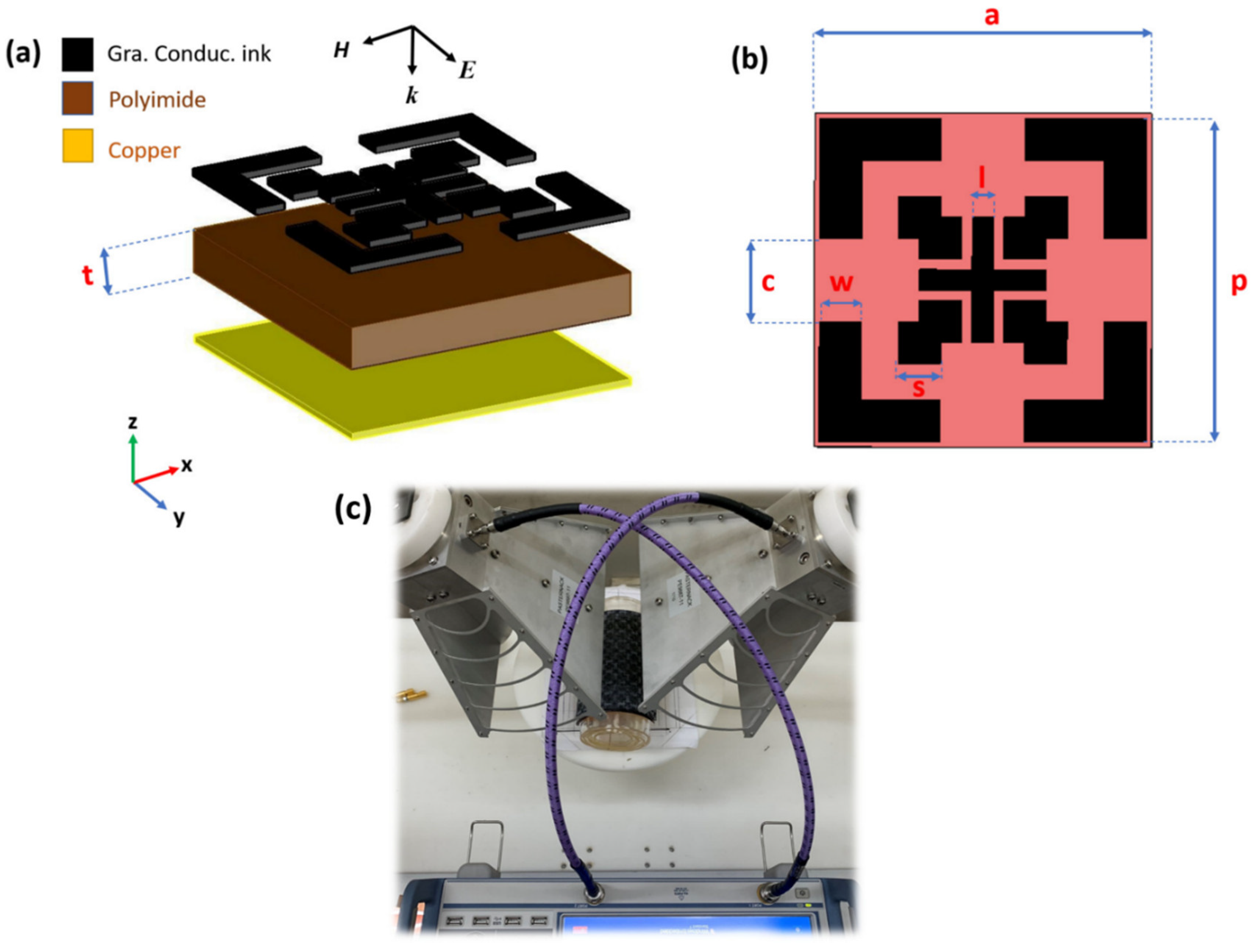
2. Materials and Methods

Figure 1 shows the geometrical parameters of proposed FBMPA, which were designed with the commercial CST software. The unit cell consists of three layers: a printed conductive–graphene ink for impedance matching, a dielectric layer and a continuous metallic plate. In simulation, the pasted conductive–graphene ink layer was modeled as a resistive sheet with a thickness of 0.036 mm. The dielectric layer is a flexible polyimide with a dielectric constant of 3.5 and a loss tangent of 0.0027 for a thickness of 2.5 mm. The bottom layer is covered with a continuous copper sheet, whose thickness and conductivity are 0.036 mm and σ = 5.8 × 10⁷ S/m, respectively. The optimized parameters are a = 16.0, p = 15.5, c = 4.0, w = 2.0, l = 1.0, and s = 2.0 mm.
The unit cell was set with periodic boundary conditions in the x-y plane, and the z axis was set to be open. A normal-incident plane wave propagated along the z direction, with the electric component along the y direction and the magnetic field along the x axis. The numerical simulation was done with CST Microwave Studio software [22].
The absorption of MPA is calculated from the transmission and the reflection: A = 1 R T = 1 | S 11 | 2 | S 21 | 2 , where A is the absorption, and R = | S 11 | 2 , T = | S 21 | 2 and S 11 , S 21 are the reflection, transmission and the reflection, transmission coefficient, respectively. The continuous copper sheet for the bottom layer allows the transmission to be ignored (i.e., T = 0) so that the absorption expression becomes A = 1 R = 1 | S 11 | 2 . The absorption can be, then, calculated simply by measuring the reflection coefficient S 11 . The fractional bandwidth (FBW), which indicates the quality of performance for the proposed FBMPA, is also evaluated by F B W ( % ) = 2 [ ( f h i g h f l o w ) / ( f h i g h + f l o w ) ] × 100 , where at the lowest (flow) and highest (fhigh) frequencies where the absorption is over 90%.
A prototype of the structure was fabricated to demonstrate the performance of proposed FBMPA. The conductive–graphene ink was printed by screen printing. The employed conductive-graphene ink was a commercial product by Dycotec Materials Ltd. [23]. The measurement setup is shown in Figure 1c. A pair of horn antennas working as transmitter/receiver was connected to a VNA (vector network analyzer) to measure the reflectance of the sample. In the measurement process, the reflection coefficient of a copper plate with the same size as the FBMPA sample was measured first for the calibration. Then, the sample was placed at that exact location to be measured. The measurement was conducted from 5 to 18 GHz.

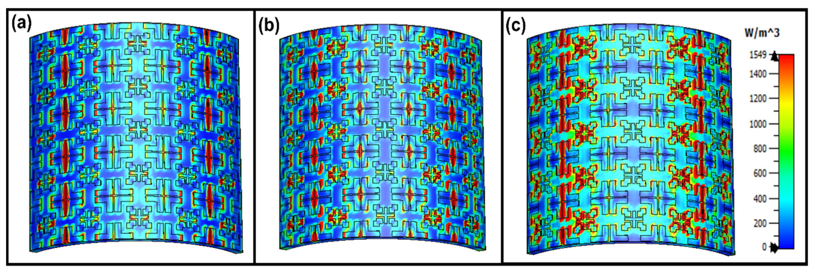
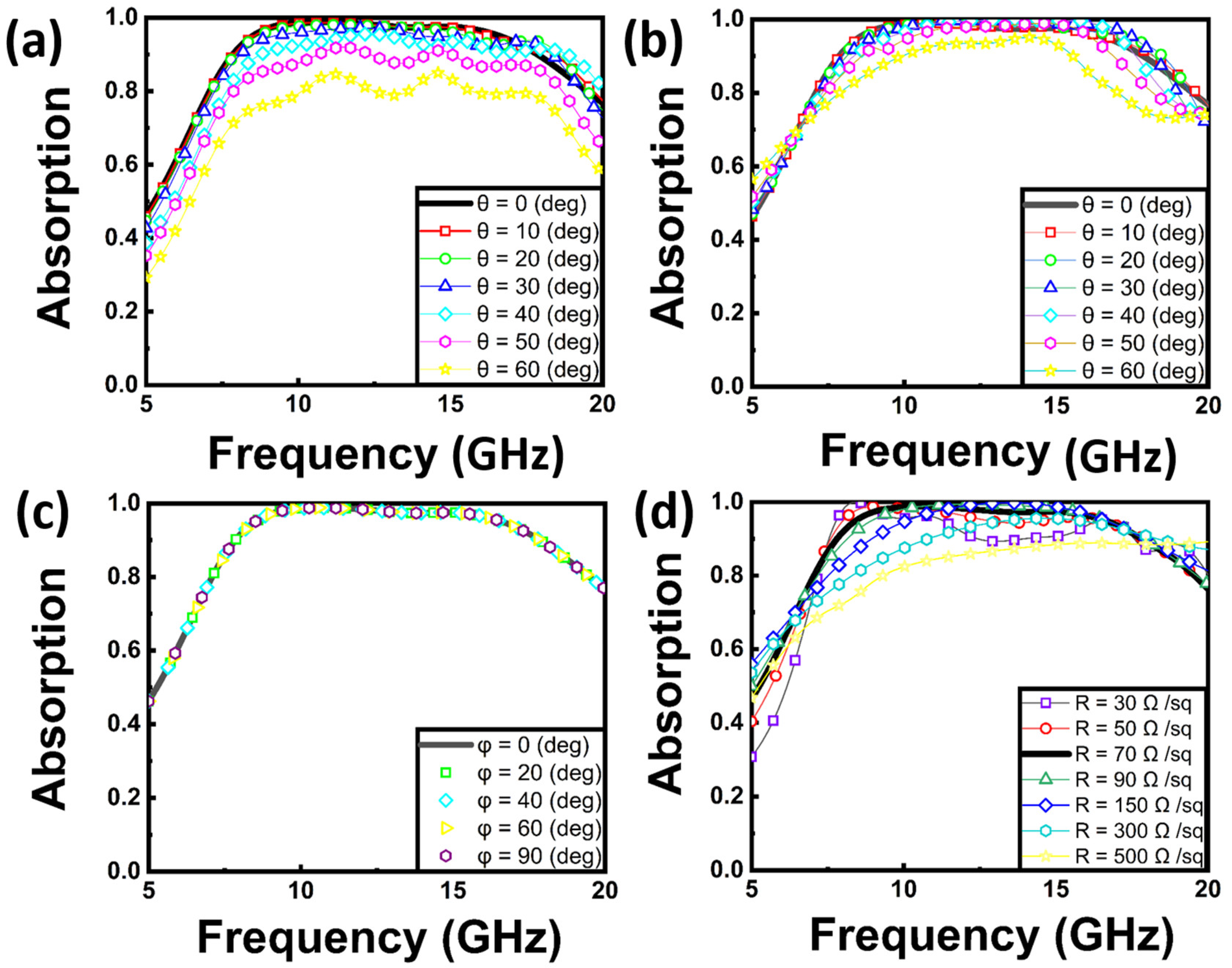
3. Results and Discussion

Figure 2a shows the simulated and measured absorption spectra of FBMPA with a sheet resistance of 70 Ω/sq. The simulated absorption spectrum is seen to be broader in a frequency range from 7.88 to 18.01 GHz with an absorption above 90%, indicating an absolute bandwidth of 10.13 GHz and an FBW of 78.25%. The measured absorption is quite similar to the simulated one. The slight difference might be caused by the surface roughness of the conductive-graphene ink layer. Figure 2b exhibits the spectra of the bent broadband perfect absorber (BBMPA) structure with a radius of 40 mm. The simulated absorption exceeds 90% from 6.7 to 19.8 GHz (FBW = 98.88%). The measured result indicates a good agreement with the simulated one.
To gain insight into the absorption mechanism of FBMPA, Figure 3 shows the distribution of magnetic-energy density and surface power-loss density in the conductive-ink layer (for the TE polarization) at absorption frequencies of 9.2, 13.0, and 18.2 GHz. The surface currents at the top and bottom are anti-parallel to each other, confirming that strong magnetic resonances are excited and play a dominant role for the high absorption. From the distribution in Figure 3a, at a frequency of 9.2 GHz, we observe that the magnetic-energy and surface power-loss densities are mainly concentrated on the resonant rings. Figure 3b,c depict the magnetic-energy density and surface power-loss one in the conductive-graphene ink layer at 13.0 and 18.2 GHz, respectively. At 13.0 GHz, the energy is strongly dissipated in the plus-shaped resonator, while at 18.2 GHz, the energy loss is located mainly in the double-square structures. Hence, the broadband-absorption spectrum of FBMPA can be explained by the efficient combination of these three kinds of constitutive resonances. Each kind of resonance element activates two main absorption peaks. By using the low-conductivity graphene ink (compared with that of the conventional metal), these peaks are broadened to the extent that they overlap and enhance each other. Consequently, a high absorption (over 90%) is achieved over a wide band. In other words, both Ohmic loss (in the conductive-ink layer) and dielectric one are the origin of broadband absorption inside the proposed FBMPA. It can be noted that these power-loss distributions are formed in both dielectric (Pd) and conductive-ink (Pm) layers, which can be expressed by
P d = π ε f t a n δ V d   | E 2 | d V
and
P m = 1 2 π μ f σ S m   | H 2 | d S .
In Equations (1) and (2), V d , ε and t a n δ are the volume, permittivity and tangential loss, respectively, of the dielectric layer. S m , μ, and σ are the surface area, permeability and conductivity, respectively, of the conductor layer. f, E and H are the frequency, electric and magnetic field of incident-plane wave, respectively [24]. It can be concluded that, in the case of the FBMPA, the consumed energy is mainly dissipated in the conductive layer rather than in the dielectric one, as shown by the magnitude of power-loss densities in Figure 3.
For the BBMPA (with a bending radius of 40 mm), the distributions of power-loss density at absorption frequencies of 9.2, 13.0 and 18.2 GHz are slightly changed, as illustrated in Figure 4. At 9.2 GHz, the power-loss density is concentrated on the outer edges of resonant-ring structures. This is noticed mainly on the outer edges of resonant rings and also the plus-shaped resonators at 13.0 GHz, and distributed on all three constitutive resonators at 18.2 GHz. Remarkably, the power loss dissipated in the dielectric and low-conductivity layers contributes simultaneously to the total absorption of BBMPA [24]:
A = P m + P d P i n   and   P i n = R l η 0 , ,
where A is the power captured by the BBMPA. η 0 = μ 0 ε 0 = 120 π     and Pin are the wave impedance of vacuum and the time averaged incident power to the BBMPA, respectively. R and l are the radius and height of cylinder, respectively. Therefore, the power-loss density distributions are only concentrated around the curved sub-areas, which are symmetric about the E-field axis, as shown in Figure 4.
The dependence of absorption behavior on the polarization and incident angle of the incoming wave is also investigated for the FBMPA, as presented in Figure 5. Figure 5a,b show the absorption is inversely proportional to the incidence angle in both cases of TE and TM polarizations. Obviously, the absorption spectra remain relatively stable with an increase of the incident angle up to 30° for the TE mode. Even when the incident angle is increased to be 60°, the absorption is still over 70%, which also covers a wide frequency range from 7.7 to 18.9 GHz. For the TM mode, the FBW of absorption spectra drops from 78.25% to 41.6% as the incident angle reaches 60° from the normal. For both cases, the mismatched impedance between the FBMPA and the surrounding environment reduces the absorption for higher incident angles. Figure 5c shows the independence of absorption spectra of the polarization angle. Since the polarization angle is changed from 0 to 90° (in case of the normal incidence), an FBW of 78.25% for the absorption spectra remains unchanged owing to the symmetric constituent resonances.
An advantage of the conductive ink over the conventional metallic material is that we can manipulate easily the sheet resistance and the conductivity of layer. The sheet resistance of conductive-graphene ink can be engineered to suit a particular application by adding functional materials (such as binder, dispersant, surfactant, slip agent, and more). The absorption characteristics of BBMPA depend on the sheet resistance of conductive ink as indicated in Figure 5d. The simulated results show that the low resistance gives rise to multi-peak absorption while the high one leads to a wide-band absorption. The local absorption is maximized when the sheet resistance comes to be 30 Ω/sq. However, the widest-band absorption (with an absorption higher than 90%) is obtained for a sheet resistance of 70 Ω/sq. When the sheet resistance of graphene ink is increased to be 500 Ω/sq., the absorption is reduced to be roughly 80% in the frequency range of interest.
For the practical applications, the absorbers should be flexible mechanically to cover different shaped objects. The absorption of the cylindrical-absorber model (for vertically-polarized incident wave) was simulated and shown in Figure 6 to study the absorption performance of BBMPA. To simulate the curved BMPA, we construct a full structure instead of the unit cell, as shown in Figure 6a. A normal-incident plane wave propagates along the z direction, with the electric field along the y axis and the magnetic one along the x direction. Figure 6b illustrates the simulated absorption for the bent-absorber model with different bending radii in the range of 40–500 mm. When the bending radius is 500 mm, the curved structure is nearly planar; the absorption spectrum is almost identical to that of the planar structure. As the bending radius decreases from 500 to 80 mm, the absorption in a frequency region from 16 to 20 GHz is enhanced. Then it is reduced gradually when it keeps decreasing from 80 to 40 mm. It is noteworthy that when the bending radius decreases from 80 to 40 mm, the low-frequency edge of absorption spectrum is also changed. The absorption around 7.5 GHz is enhanced while that around 9 GHz is reduced when the MPA is bent further, meaning that the low-frequency edge of the absorption spectrum is not totally flat any more. The absorption band exceeds 95% with an FBW over 80% for all bending radii. The fact that we can achieve robust broadband absorption in the presence of deformation suggests these flexible absorbers might be well suited for many practical applications.
Finally, in order to demonstrate the advantages of proposed absorber over other similar structures, the performance characteristics of the proposed structure are compared with recently-reported broadband absorbers by using conductive ink as shown in Table 1.
The absorbers in Refs. [25,26,27] have a large bandwidth, but are thick and not flexible. The absorbers presented in Refs. [28,29,30] are all flexible, but either require more complicated fabrication process due to the multilayer stack-up structure as in Refs. [29,30] or have a small FBW like in Ref. [28]. The proposed FBMPA shows a good balance among large FBW, small thickness and flexibility.

4. Conclusions

A flexible broadband metamaterial perfect absorber based on conductive-graphene ink, integrated on a polyimide substrate, was characterized for both flat and bending states. The magnetic resonances in both planar and cylindrical resonators gave rise to a broadband absorption of 90% in a greatly-wide frequency range (FBW = 78.25% for the FBMPA and FBW over 80% for the BBMPA). Furthermore, the proposed BMPA works stably with respect to the incident angle (up to 30° in the TE mode and 60° in the TM mode). These results suggest our proposed flexible and broadband metamaterial perfect absorbers could be appropriate for the commercial applications involving next generation of flexible, ultra-broadband, polarization/oblique-incidence insensitive, low-cost, and ultrathin-wearable electromagnetic absorbers in near future.

Author Contributions

L.V.L., B.X.K., Y.L., V.D.L. and H.Z. conceived the idea. The electromagnetic simulation and calculation were carried out by N.S.K., B.S.T., N.T.T., T.T.G., P.T.S., Y.L. and L.C., L.V.L., B.X.K., Y.L. and V.D.L. analyzed and wrote the article. All of the authors discussed and commented on the manuscript. All authors have read and agreed to the published version of the manuscript.

Funding

This research is funded by Vietnam National Foundation for Science and Technology Development (NAFOSTED) under grant number 103.99-2020.23 and by Korea Evaluation Institute of Industrial Technology (Project No. 20016179).

Data Availability Statement

The data presented in this paper are available on request from the corresponding author.

Conflicts of Interest

The authors declare no conflict of interest.

References

  1. Smith, D.R.; Padilla, W.J.; Vier, D.; Nemat-Nasser, S.C.; Schultz, S. Composite medium with simultaneously negative permeability and permittivity. Phys. Rev. Lett. 2000, 84, 4184. [Google Scholar] [CrossRef] [Green Version]
  2. Duan, Z.; Tang, X.; Wang, Z.; Zhang, Y.; Chen, X.; Chen, M.; Gong, Y. Observation of the reversed Cherenkov radiation. Nat. Commun. 2017, 8, 14901. [Google Scholar] [CrossRef]
  3. Seddon, N.; Bearpark, T. Observation of the inverse Doppler effect. Science 2003, 302, 1537. [Google Scholar] [CrossRef]
  4. Landy, N.I.; Sajuyigbe, S.; Mock, J.J.; Smith, D.R.; Padilla, W.J. Perfect metamaterial absorber. Phys. Rev. Lett. 2008, 100, 207402. [Google Scholar] [CrossRef]
  5. Rosenberg, J.; Shenoi, R.V.; Vandervelde, T.E.; Krishna, S.; Painter, O.A. A multispectral and polarization-selective surface-plasmon resonant midinfrared detector. Appl. Phys. Lett. 2009, 95, 161101. [Google Scholar] [CrossRef] [Green Version]
  6. Yu, Z.; Veronis, G.; Fan, S.; Brongersma, M.L. Design of midinfrared photodetectors enhanced by surface plasmons on grating structures. Appl. Phys. Lett. 2006, 89, 151116. [Google Scholar] [CrossRef] [Green Version]
  7. Liao, Y.L.; Zhao, Y. Ultra-narrowband dielectric metamaterial absorber with ultra-sparse nanowire grids for sensing applications. Sci. Rep. 2020, 10, 1–7. [Google Scholar] [CrossRef] [PubMed] [Green Version]
  8. Tao, R.; Zahertar, S.; Torun, H.; Liu, Y.R.; Wang, M.; Lu, Y.; Fu, Y.Q. Flexible and integrated sensing platform of acoustic waves and metamaterials based on polyimide-coated woven carbon fibers. ACS Sens. 2020, 5, 2563–2569. [Google Scholar] [CrossRef] [PubMed]
  9. Feng, H.; Li, X.; Wang, M.; Xia, F.; Zhang, K.; Kong, W.; Yun, M. Ultrabroadband metamaterial absorbers from ultraviolet to near-infrared based on multiple resonances for harvesting solar energy. Opt. Express 2021, 29, 6000–6010. [Google Scholar] [CrossRef] [PubMed]
  10. Elsharabasy, A.; Bakr, M.; Deen, M.J. Wide-angle, wide-band, polarization-insensitive metamaterial absorber for thermal energy harvesting. Sci. Rep. 2020, 10, 1–10. [Google Scholar] [CrossRef]
  11. Iwaszczuk, K.; Strikwerda, A.C.; Fan, K.; Zhang, X.; Averitt, R.D.; Jepsen, P.U. Flexible metamaterial absorbers for stealth applications at terahertz frequencies. Opt. Express 2012, 20, 635–643. [Google Scholar] [CrossRef] [PubMed] [Green Version]
  12. Zhou, B.C.; Wang, D.H.; Ma, J.J.; Li, B.Y.; Zhao, Y.J.; Li, K.X. An ultrathin and broadband radar absorber using metamaterials. Waves Random Complex Media 2019, 31, 1–10. [Google Scholar] [CrossRef]
  13. Kim, J.; Han, K.; Hahn, J.W. Selective dual-band metamaterial perfect absorber for infrared stealth technology. Sci. Rep. 2017, 7, 1–9. [Google Scholar] [CrossRef]
  14. Landy, N.; Bingham, C.; Tyler, T.; Jokerst, N.; Smith, D.; Padilla, W. Design, theory, and measurement of a polarization-insensitive absorber for terahertz imaging. Phys. Rev. B 2009, 79, 125104. [Google Scholar] [CrossRef] [Green Version]
  15. Sadeqi, A.; Nejad, H.R.; Sonkusale, S. Low-cost metamaterial-on-paper chemical sensor. Opt. Express 2017, 25, 16092–16100. [Google Scholar] [CrossRef] [PubMed]
  16. Xin, W.; Binzhen, Z.; Wanjun, W.; Junlin, W.; Junping, D. Design, fabrication, and characterization of a flexible dual-band metamaterial absorber. IEEE Photonics J. 2017, 9, 1–12. [Google Scholar] [CrossRef]
  17. Dayal, G.; Ramakrishna, S.A.J. High temperature VO2 based microbolometer with enhanced light absorption. Phys. D Appl. Phys. 2014, 48, 035105. [Google Scholar] [CrossRef]
  18. Kim, H.K.; Ling, K.; Kim, K.; Lim, S. Flexible inkjet-printed metamaterial absorber for coating a cylindrical object. Opt. Express 2015, 23, 5898–5906. [Google Scholar] [CrossRef]
  19. Nguyen, T.Q.H.; Nguyen, T.K.T.; Cao, T.N.; Nguyen, H.; Bach, L.G. Numerical study of a broadband metamaterial absorber using a single split circle ring and lumped resistors for X-band applications. AIP Adv. 2020, 10, 035326. [Google Scholar] [CrossRef]
  20. Li, S.J.; Wu, P.X.; Xu, H.X.; Zhou, Y.L.; Cao, X.Y.; Han, J.F.; Zhang, Z. Ultra-wideband and polarization-insensitive perfect absorber using multilayer metamaterials, lumped resistors, and strong coupling effects. Nanoscale Res. Lett. 2018, 13, 1–13. [Google Scholar] [CrossRef] [PubMed]
  21. Miles, V.B.; Xian, C.X.; Yang, Y.C.; Shun, Z.; Jizhou, S.; Guoliang, H.J. Experimental demonstration of a dissipative multi-resonator metamaterial for broadband elastic wave attenuation. Sound Vib. 2019, 438, 1–12. [Google Scholar]
  22. CST Microwave Studio 2015, License ID: 52856-1. Dassault Systèmes. Available online: http://www.cst.com (accessed on 15 June 2021).
  23. Dycotec Materials Ltd-Industrial Estate. Unit 6 Stanier Rd. Porte Marsh Rd. Calne SN11 9PX. United Kingdom. Available online: https://www.dycotecmaterials.com/ (accessed on 1 July 2021).
  24. Balanis, C.A. Advanced Engineering Electromagnetics; John Wiley and Sons: Hoboken, NJ, USA, 1989. [Google Scholar]
  25. Fang, W.; Zhou, F.-K.; Wang, Y.-J.; Chen, P. Broadband, wide-angle, polarization-independent and lightweight low-scattering coding metamaterial based on stereo meta-atoms. Results Phys. 2021, 20, 103687. [Google Scholar] [CrossRef]
  26. Yanjie, W.; Hai, L.; Jie, X.; Junjie, H.; Rui, Z.; Feng, D.; Rongxin, T.J. A broadband metamaterial absorber design using characteristic modes analysis. Appl. Phys. 2021, 129, 134902. [Google Scholar]
  27. Guangsheng, D.; Kun, L.; Hanxiao, S.; Yuan, H.; Xiaoying, Z.; Zhiping, Y.; Jun, Y. Wideband absorber based on conductive ink frequency selective surface with polarization insensitivity and wide-incident-angle stability. Nanomater. Nanotechnol. 2020, 10, 1847980420935718. [Google Scholar]
  28. Mohammad, M.N.; Seyed, M.B.; Mohsen, H.; Masoud, M. Ink-jet printed metamaterial microwave absorber using reactive inks. Int. J. Electron. Commun. 2020, 123, 153259. [Google Scholar]
  29. Manish, M.T.; Nisha, G. Broadband Polarization-Insensitive Inkjet-Printed Conformal Metamaterial Absorber. IEEE Trans. Electromagn. Compat. 2021, 1–8. Available online: https://ieeexplore.ieee.org/abstract/document/9502159 (accessed on 1 July 2021).
  30. Guangsheng, D.; Kun, L.; Hanxiao, S.; Yuan, H.; Xiaoying, Z.; Zhiping, Y.; Ying, L.; Jun, Y. An ultra-wideband, polarization insensitive metamaterial absorber based on multiple resistive film layers with wide-incident-angle stability. Int. J. Microw. Wirel. Technol. 2021, 13, 58–66. [Google Scholar]
Figure 1. (a) Schematic of the three-dimensional unit cell and (b) the top view of FBMPA structure. (c) The measurement setup.
Photonics 08 00440 g001
Figure 2. Simulated and measured absorption spectra of the (a) FBMPA and (b) BBMPA structure (a bending radius of 40 mm).
Photonics 08 00440 g002
Figure 3. Three-dimensional distribution of the magnetic-energy density in the dielectric layer (top) and the surface power-loss one (bottom) of MPA structure at (a) 9.2, (b) 13.0, and (c) 18.2 GHz (for the TE polarization).
Photonics 08 00440 g003
Figure 4. Distribution of the power-loss density of BBMPA structure at (a) 9.2, (b) 13.0, and (c) 18.2 GHz (at a bending radius of 40 mm) (for the TE polarization).
Photonics 08 00440 g004
Figure 5. Simulated absorption results for the obliquely-incident angles of (a) TE- and (b) TM-polarized incident wave, according to (c) polarization angle and (d) resistance of the conductive-graphene ink sheet.
Photonics 08 00440 g005
Figure 6. Full-structure of the BBMPA and dependence of the simulated absorption spectrum on bending radius.
Photonics 08 00440 g006
Table 1. Performance comparison of the proposed FBMPA with recently-reported MPAs by using conductive ink.
ReferenceOperating Frequency (GHz)Bandwidth (GHz)
(Absorption over 90%)
FBW (%) (Absorption over 90%)Thickness (mm)Number of Dielectric LayersFlexible
[25]12–231162.8661 (stereo structure)no
[26]3.21–14.3511.14126.889.22no
[27]6.58–16.389.885.43.31no
[28]6.66–7.040.385.557.21yes
[29]8.43–10.381.9520.731.064yes
[30]2.34–18.9516.6115611.33yes
This work7.88–18.0110.1378.252.51yes
Publisher’s Note: MDPI stays neutral with regard to jurisdictional claims in published maps and institutional affiliations.

