Article

Study of an Integration Platform Based on an Adiabatic Active-Layer Waveguide Connection for InP Photonic Device Integration Mirroring That of Heterogeneous Integration on Silicon

1
Department of Electrical & Computer Engineering, Northwestern University, Evanston, IL 60208, USA
2
State Key Laboratory of Integrated Optoelectronics, College of Electronic Science and Engineering, Jilin University, 2699 Qianjin Street, Changchun 130012, China
3
School of Optical and Electronic Information, Huazhong University of Science and Technology, Wuhan 430074, China
4
OptoNet Inc., Evanston, IL 60201, USA
5
Key Laboratory of Supramolecular Structure & Materials, College of Chemistry, Jilin University, 2699 Qianjin Street, Changchun 130012, China
6
Wuhan National Laboratory for Optoelectronics (WNLO), Huazhong University of Science and Technology, Wuhan 430074, China
*
Authors to whom correspondence should be addressed.
Changming Chen and Junyu Li are co-first authors of the article.
Photonics 2021, 8(10), 433; https://doi.org/10.3390/photonics8100433
Submission received: 23 August 2021 / Revised: 24 September 2021 / Accepted: 7 October 2021 / Published: 9 October 2021
(This article belongs to the Special Issue Silicon Based Integrated Optics)

Abstract

:
In this work, a photonic device integration platform capable of integration of active-passive InP-based photonic devices without the use of material regrowth is introduced. The platform makes use of an adiabatic active-layer waveguide connection (ALWC) to move an optical beam between active and passive devices. The performance of this platform is analyzed using an example made up of four main sections: (1) a fiber coupling section for enabling vertical beam coupling from optical fiber into the photonic chip using a mode-matched surface grating with apodized duty cycles; (2) a transparent waveguide section for realizing passive photonic devices; (3) an adiabatic mode connection structure for moving the optical beam between passive and active device sections; and (4) an active device section for realizing active photonic devices. It is shown that the coupled surface grating, when added with a bottom gold reflector, can achieve a high chip-to-fiber coupling efficiency (CE) of 88.3% at 1550 nm. The adiabatic active-layer mode connection structure has an optical loss of lower than 1% (CE > 99%). The active device section can achieve an optical gain of 20 dB/mm with the use of only 3 quantum wells. The optimized structural parameters of the entire waveguide module are analyzed and discussed.

1. Introduction

The III-V semiconductor-based photonic integrated circuits are playing key roles in optical communication systems [1,2,3,4,5]. A few commonly used methods for active-passive III-V semiconductor (e.g., InP/GaAs) photonic device integration include the material regrowth approach [6], vertical twin-guide method without the need for material regrowth [7], and quantum well intermixing (QWI) method [8]. Each method has its own pros and cons. The latter two methods have the advantage of not involving the relatively tedious and expensive material regrowth processes. However, they are more limited in their capabilities compared with the material regrowth method. Thus, each method has its own area of applicability.
Recently, with the advancements of silicon photonics, another active-passive photonic device integration method was introduced, based on wafer bonding of a III-V semiconductor to silicon, enabling the transfer of a thin layer of epitaxial III-V semiconductor material on top of silicon, referred to as heterogenous integration of III-V semiconductor materials on silicon [9,10,11]. This method enables the passive photonic devices to be fabricated on the top silicon layer of a Silicon-on-Insulator (SOI) substrate and the active InP-based devices to be fabricated on the bonded epitaxial layer. In addition, typical optical coupling from the passive silicon waveguide to an optical fiber is usually performed with the use of a surface grating [12,13,14]. Aside from its compatibility with silicon photonics, from an active-passive photonic device integration viewpoint, this approach has a few advantages in that the silicon has relatively low optical absorption, so low-loss passive photonic devices can be fabricated. The surface grating can also be fabricated on the silicon waveguide, enabling optical beam coupling from chip to fiber in a convenient way anywhere inside the photonic chip area (i.e., the coupling does not have to be at the chip’s edge). In addition, strong-guiding waveguides can be fabricated on the silicon layer, enabling compact photonic devices to be realized.
In this paper, we explore an active-passive photonic device integration approach motivated by the “heterogeneous integration method” mentioned above in terms of an active-passive device connection and optical fiber coupling but as a purely InP-based integration platform. We analyze its feasibility in detail using a specific example. We show that this platform can harbor similar advantages to those of the heterogeneous integration method but can be applied to pure InP-based photonic integrated circuits. Compared with “heterogeneous integration of InP devices on silicon,” pure InP-based photonic integration does not need wafer bonding. Note that typically, no single photonic integration is good for all applications. Which method is preferred is dependent on the specific application involved.
As described below, one key difference between this approach and the vertical twin-guide approach is that the beam from the passive device region is brought into the active device region via an adiabatic mode-connecting structure, connecting basically the same waveguide core. More specifically, the optical beam in the passive device region is propagated in the same waveguide core layer as that used for the active device region that contains an active material layer (e.g., the layer with quantum wells that gives optical gain and absorption). In the active device region, the active material layer is placed at the top of the waveguide core. In the passive device region, the active material layer is etched away, leaving only the transparent waveguide core that is typically undoped. The top p-doped structure in the active device region that has high optical absorption is also etched away in the passive device region so that it will not contribute to the optical loss. Thus, the coupling from the passive device region into the active device region with the active material layer is comparatively easier to achieve than that for the twin-guide case and is similar to the evanescence coupling scheme used in “heterogeneous integration of InP devices on silicon”, which involves the use of an adiabatic coupler to bring the optical beam from the passive silicon waveguide into the active gain material region. Note that just like the evanescent vertical coupling used in “heterogeneous integration of InP devices on silicon” case that is relatively insensitive to small misalignments [15], the vertical evanescence coupling or other adiabatic coupling structures used here would also be relatively insensitive to small fabrication misalignments. Furthermore, the approach explored here includes the use of a surface grating to couple light from the passive optical waveguide on the chip to an optical fiber. We showed that with a proper design, high coupling efficiency between the waveguide and optical fiber can be achieved.
We refer to the platform we introduce here as the adiabatic active-layer waveguide connection (ALWC)-based active-passive photonic device integration method to distinguish it from the vertical twin-guide method of previous works.

2. Design and Simulation

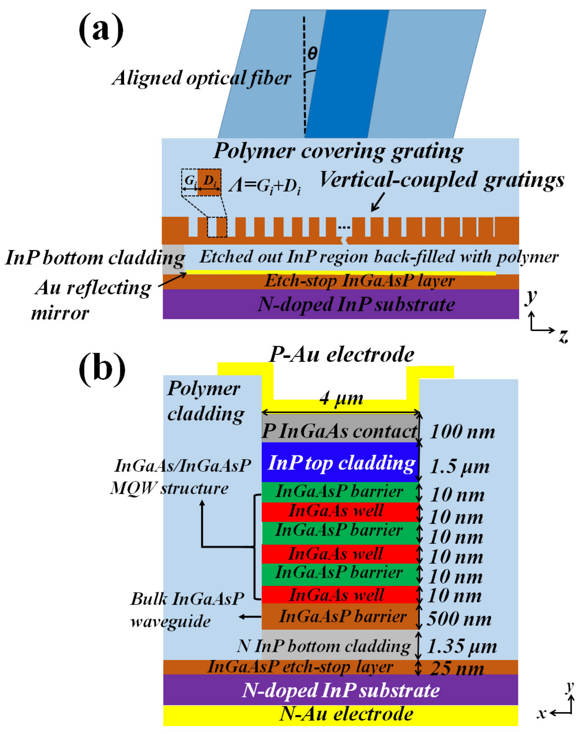
2.1. Overall Description of an Integrated Structure as an Example

We illustrate the platform using the case of an optical amplifier integrated with a passive waveguide and the incorporation of a surface grating to couple light between the waveguide and an optical fiber. The schematic of the entire integrated device structure is shown in Figure 1a,b.
As shown by Figure 1, the entire structure is divided into four sections. In Section A (fiber-coupling structure), an optical beam with a wavelength centered at 1550 nm launched by an aligned optical fiber is first coupled vertically through a surface grating structure into a transparent waveguide made of 500-nm thick undoped InGaAsP materials (with a bandgap wavelength at 1.25 μm so that it is transparent at the 1550-nm wavelength range). The width of this waveguide with the surface grating is ~15 μm so that the beam from the optical fiber with the typical 8.2-μm core diameter, giving a mode diameter of 7.2 μm (measured at 1/e point of the intensity profile), can be captured efficiently into the lowest order mode of the 15-μm side strong-guiding waveguide (i.e., the 7.2-μm 1/e mode width gives the maximum field overlap with the lowest-order mode in the 15-μm wide strong-guiding waveguide). The 15-μm wide waveguide is then tapered down horizontally to a width of 4 μm. The 4-μm wide waveguide then acts as a channel waveguide to bring the beam into the next device section. As explained below, the InP material under this 500-nm thick InGaAsP layer is removed (e.g., via a selective chemical etchant such as HCL that will etch away the InP material without etching the InGaAsP material) and filled with n~1.5 polymer as the “lower cladding”. The space between the surface grating and the fiber is also filled with n~1.5 polymer. Note that the choice of the 4-μm waveguide width and other similar choices made below are somewhat flexible.
In Section B (passive waveguide device), the light beam from Section A is propagated into a 4-μm wide, 500-nm thick InGaAsP passive waveguide core. In this region, the material under this 500-nm thick InGaAsP layer has InP material as the lower cladding (i.e., not polymer). To minimize the optical loss when the beam enters from Section A, which has polymer lower cladding, into this region, which has InP as the lower cladding, a tapering structure at the lower InP cladding is used. As described later, this tapering structure underneath the InGaAsP waveguide core is made via photolithography patterning and selective chemical wet etching. The transparent waveguide structure in Section B can be used to make various passive photonic devices, such as optical beam couplers and beam splitters. In this paper, we show it as a transparent waveguide for illustration purposes (see Section 2.6 for further elaborations on this).
The beam from the passive photonic device in Section B is then brought into Section C via a 4-μm wide connecting waveguide. In Section C (active-passive waveguide connection), the beam is made to slowly connect into an active gain material region through the use of an adiabatic taper structure on top of the 500-nm thick InGaAsP layer (with the bandgap wavelength at 1.25 μm), which is the 4-μm wide connecting channel waveguide from Section B. At the taper, the 500-nm thick InGaAsP waveguide then becomes part of the waveguide core, complete with quantum wells immediately at the top of the 500-nm thick InGaAsP layer, forming a gain waveguide core with a total thickness of 560 nm (the multiple quantum well (MQW) region with three quantum wells immediately on top of the 500-nm thick InGaAsP layer is 60 nm thick). Above this gain waveguide core is 1500-nm thick, lightly P-doped InP material, forming a P-doped top waveguide cladding followed by a 100-nm thick, highly P-doped InGaAs layer that forms the P-ohmic contact layer at the top surface. Below the 560-nm gain waveguide core is a 1350-nm thick, moderately N-doped InP layer forming the lower waveguide cladding. This 1350-nm thick N-doped InP layer also serves as the N-ohmic contact layer. Right below this N-doped InP layer is a 25-nm thick N-doped InGaAsP layer (with the bandgap wavelength at 1.25 μm) that serves as an “etch-stop layer”, whose function will be explained in more detail below. Basically, it is used for optimizing the fiber-coupling grating performances. This tapering structure of Section C acts as an adiabatic mode connection structure to connect the lowest-order mode from the passive waveguide structure of Section B to the lowest-order mode in the active gain waveguide structure of Section D.
After Section C’s taper, in Section D (active waveguide device), the beam enters into the active gain material region. The waveguiding structure with optical gain material in Section D can be used to make an optical amplifier, light-emitting device, laser, optical switches, or a modulator, depending on the application. If needed, the beam in Section D can be transmitted to the next device by connecting Section D’s output to another passive waveguide device section (called Section F) similar to that of Section B via an active-passive waveguide connection section (called Section E), similar to the tapering structure of Section C but oriented in the opposite direction so that the upper part is tapered down to a point from Section D toward Section F. The beam from the active waveguide device section of Section D can then be smoothly propagated into the passive waveguide device section of Section F without much optical loss.
The above layered structure is summarized by Table 1. The “top view” given by an X-Z horizontal cross-section of the entire structure encompassing Sections A–D is shown in Figure 1b. As shown in Figure 1b, W1 is the width of the vertically coupled apodized grating and W2 is the width of the InGaAsP channel waveguide. L1 + L2 is the length of the grating structure plus the length of a 15-μm wide connecting waveguide (with polymer as the lower cladding), L3 is the length of the horizontal taper after the grating (tapering from 15 μm to 4 μm horizontally), L4 + LBT is the length of a 4-μm wide connecting waveguide (with polymer below) plus the length of a “bottom taper” involving the lower InP cladding, L5 + LT is the lengths of the 4-μm wide connecting waveguide (with InP cladding below) plus a “top taper” involving the top MQW+InP structure, and L6 is the length of the MQW active waveguide device section. Section A is formed by L1 + L2 + L3; Section B is formed by L4 + LBT; Section C is formed by L5 + LT; and Section D is formed by L6. As shown in Figure 1a,b, the InGaAs/InGaAsP MQW structure is constructed on top of the passive 500-nm thick InGaAsP waveguide. The ohmic contact electrodes are formed on the N- and P-ohmic contact regions. The detailed parameters such as the doping type, thickness, refractive index at a 1550-nm wavelength, and the carrier concentration for each semiconductor layer of the MQW gain waveguide structure are given in Table 1. The Y-Z (vertical-lateral) cross-sectional drawing for the vertically coupled apodized optical grating region and the Y-X (vertical-fontal) cross-sectional drawing for the active waveguide device section are shown in Figure 2a,b, respectively. Below, we describe each of the sections (A–D) in more detail.

2.2. Design for the Fiber-Coupling Structure of Section A

Below, we describe the design for the vertically coupled grating together with a suggested fabrication procedure for the design.
To realize coupling of the beam between the optical fiber and the photonic chip, a surface grating can be fabricated by first writing the grating pattern using electron beam lithography (e.g., using the 300-nm thick PMMA as the E-beam resist) on a ~150-nm thick silicon dioxide layer pre-deposited on the 500-nm thick InGaAsP waveguide surface. The grating pattern is then transferred down to the oxide layer using dry etching (e.g., using Reactive Ion Etching (RIE) with, for example, CHF3, Ar, and O2 as the reactive gasses) with the E-beam resist as the dry etching mask. The oxide layer with the transferred pattern is then used as a dry etching mask for etching vertically into the 500-nm thick InGaAsP layer (e.g., using RIE with methane-hydrogen as the reactive gasses) to form the surface grating. As an example, the etch depth into the 500-nm InGaAsP layer can be 400 nm for the gap region of the grating teeth while the ridge region of the grating teeth is unetched. Note that the grating teeth are filled with polymer (with n = 1.5), as described in more detail below.
Next, we describe the design of the grating structure. To realize high coupling efficiency between the optical fiber and coupling grating structure, the duty cycle and period Λi of the teeth in the fiber coupling grating are varied, forming an apodized grating. The design is based on Equations (1)–(4) in [16]. As shown in Figure 2a, Gi and Di (Λi = Gi + Di) are the lengths of the gap and ridge region, respectively, for each of the grating periods. The variation of the duty cycle and period enable the coupling strength for the beam energy exiting the grating to be varied along the propagation direction so that the beam intensity profile for the beam coming out of the grating and propagating toward the optical fiber will approximately match the beam shape and size of the optical beam in the single-mode optical fiber. This enables the beam from the waveguide to be efficiently coupled into the optical fiber. As light propagation is reciprocal, that means the beam from the fiber coupling into the waveguide via the surface grating will also be efficient. The specific values for Gi and Di are calculated and given in Table 2. The total length L1 and the width W1 (Figure 1b) of the grating are 20 μm and 15 μm, respectively. We call this grating which uses varying cycles to achieve mode profile shaping and mode matching the “apodized surface grating”.
The schematic diagram for the structure used for computational electromagnetic simulation of this vertically coupled InGaAsP apodized surface grating structure is shown in Figure 3a. To further enhance the coupling efficiency between the optical fiber and the chip, a gold (Au) reflecting surface is formed at a location below the grating region. This is formed by first protecting the surface of the grating region with a 1-µm thick silicon dioxide layer to give a higher mechanical strength. An opening is created on the silicon dioxide layer using photolithography. Dry etching, such as Reactive Ion Etching (e.g., using methane-hydrogen as the reactive etching gasses), is then used to vertically etch into the 500-nm thick InGaAsP waveguide core and then down into the InP material region below the waveguide core. Through the same opening, wet etching involving the use of HCL is then used to selectively wet etch away the InP material below the 500-nm thick InGaAsP waveguide core. HCL etches the InP material much faster than the InGaAsP material, so the InGaAsP waveguide core is basically unetched during the process. The 25-nm thick InGaAsP layer 1350 nm below the bottom of the 500-nm thick InGaAsP waveguide core serves as an etched stop layer, so the HCL wet etching will not penetrate below this etch stop layer and instead will form a smooth surface that is exactly 1350 nm below the bottom of the 500-nm InGaAsP waveguide core. A 100-nm thick piece of gold metal is then deposited onto the surface of this etched stop layer, forming an optical reflector. This deposition can be achieved by titling the chip during deposition so the gold will go underneath the 500-nm thick InGaAsP waveguide with surface grating (a large space is etched on both sides of the grating bridge to enable the gold deposition to go underneath). The hollowed-out bottom region of the grating is then filled with polymer by spin coating (e.g., with Benzocyclobutene (BCB) polymer or, alternatively, with the fluorinated polymer discussed below). The polymer is etched back to clear the grating surface. Any gold deposited on the silicon dioxide material on the grating can then be removed by a gold-etching chemical. After optical fiber alignment, the fiber position is fixed by epoxy so that the epoxy polymer will cover the region between the optical fiber tip and the grating surface.
We note that the removal of the InP material below the 500-nm thick InGaAsP waveguide is not just for placing the reflector. It turns out that when the reflective index of the InP is high, it makes the grating structure highly asymmetric (i.e., the refractive index above the grating waveguide is low (n~1.5), while the refractive index (n~3.1) of the InP material below the grating is too close to the refractive index of the InGaAsP waveguide core material (n~3.4) on which the grating is made). Our simulation showed that as a result of the high refractive index asymmetry, there was an unwanted diffraction order of the grating that emitted a significant amount of optical beam energy at a glancing angle close to the surface, making it impossible to obtain more than the 10% emission efficiency in the vertical direction that we wanted. Hence, in order to achieve a high vertical emission efficiency from the grating of ~50% or higher, we had to replace the material below the 500-nm InGaAsP waveguide with low-refractive index polymer.
The resulting structure showing the optical fiber, the grating, the gold reflector, and the polymer coverage is illustrated in Figure 3a. In the figure, h1, h2, h3, h4, and h5 are the thicknesses of the top polymer cladding layer (h1), InGaAsP waveguide layer with the grating structure (h2), bottom polymer cladding layer (h3), gold reflector layer (h4), and etched stop InGaAsP layer (h5). The coupling optical field distribution between the optical fiber and grating was simulated with Lumerical 2D FDTD software, assuming h1 = 2 μm, h2 = 500 nm, h4 = 100 nm, and h5 = 25 nm. The 2D FDTD simulation approximation was sufficient for the purpose of showing the basic idea of the proposed design. The result is shown in Figure 3b. It can be seen from the figure that the optical beam from the optical fiber above was coupled into the InGaAsP waveguide efficiently. The vertical beam fiber coupling efficiency (Tf) (between the waveguide and the optical fiber) as a function of the thickness h3 of the bottom polymer cladding is given in Figure 4a. More specifically, the beam-coupling efficiency curve (Tf) for the optical beam from the waveguide emitted into the fiber’s fundamental mode and the efficiency curve (Ta) for the optical beam from the waveguide emitted vertically in all directions above the grating surface are shown. Note that Ta includes the optical power emitted into the fiber’s fundamental mode and all the other spatial regions above the grating surface. It was found that when h3 was 1250 nm, the beam coupling efficiency Tf reached the maximum value (Tf = 88.3% and Ta = 95.5%). Compared with the Tf of 63% when no gold reflector was used (but still with polymer material filling the space below the grating and with the surface of the InGaAsP etched stop layer as a reflecting surface with only 15% reflectivity intensity), the fiber’s fundamental mode coupling efficiency (Tf) with the gold reflector was increased by 25%. The gold reflecting surface reflected the beam energy traveling downward from the grating, back to the grating, and then exiting the grating’s top surface. Figure 4b shows the normalized beam intensity profile (Igra) for the beam from the grating based on the FDTD simulation. It also shows a Gaussian function fitting curve (Igfi) for the beam profile Igra and the normalized beam intensity profile (Ifib) of the fiber’s fundamental mode. The 1/e width of the Gaussian fitted curve agfi (=7.4 μm) matched the beam width of the fiber mode intensity profile afib (=7.2 μm) well. The relationship between the coupling angle θ and coupling efficiency is given in Figure 4c. It was found that when θ = 10°, the coupling efficiency could reach the maximum value (with the wavelength at 1550 nm). With θ = 10°, the curve for the coupling efficiency as a function of the beam wavelength (λ) is shown in Figure 4d. It was found that the coupling efficiency reached the maximum value at the central 1550 nm wavelength, as expected from the design equations we used for designing the grating. The spectral width of the coupling efficiency curve, defined by the two points where the coupling efficiencies dropped by 30% (−1.5 dB) from the peak value, was 44 nm (in wavelength units). We found from the simulation that when the beam was launched from the optical fiber toward the surface grating, the reflection back to the optical fiber was 1.5%. When the beam was launched from the on-chip waveguide toward the grating, the reflection back to the fundamental mode of the waveguide was 2%. These levels of back reflection are low for integrated photonic chip applications.
In Section A, a light beam coupled into the 500-nm InGaAsP waveguide via the surface grating has a 1/e beam intensity width of about 7.2 μm. This 7.2-μm beam width is guided by the 500-nm thick InGaAsP waveguide with a width of 15 μm. As illustrated in Figure 5, this 15-μm waveguide width is then tapered down horizontally to about 4 μm with a tapering length L3. Figure 5a shows the transmission efficiency for the lowest-order transverse-electric (TE) mode at the initial 15-μm wide waveguide, propagating to the lowest-order transverse-electric (TE) mode at the final 4-μm wide waveguide of this tapering region as a function of the tapering length L3. Note that TE mode has an electric field pointing in the planar or horizontal direction. This efficiency is referred to as the “lowest-order TE-mode connection efficiency”, or simply as the “mode connection efficiency”, which will also be the case for all the other tapering sections described below. The figure shows that an efficiency of 98.5% can be achieved at L3 = 240 μm. Figure 5b,c shows the optical mode at the input and output regions of this taper. Figure 5d shows a horizontal cross-section illustrating the behavior of the propagating beam in the taper with L3 = 240 μm.
To reduce the optical absorption loss and improve the thermal stability of the fiber-mode coupling gratings, instead of using BCB polymer, highly fluorinated polymer can be used as the cladding material above and below the grating, which is composed of fluorinated bis-phenol-A novolac resin (FSU-8) and fluorinated, epoxy-terminated, low-molecular-weight bisphenol A polycarbonate (FBPA-PC EP). The fluorinated polymer has low optical absorption loss at the 1550-nm wavelength range due to reduced vibration overtone by replacing the C-H bonds with C-F bonds [17,18]. More importantly, the polymer material, when used for covering the InGaAsP grating teeth, can help to lower the temperature dependence of the grating coupling wavelength, making it athermal. As the coefficient of thermal expansion (CTE) of the InGaAsP guiding layer is positive while the thermo-optic coefficient of the fluorinated polymer covering layer is negative, the fluorinated polymer can be used to reduce the wavelength shift of the grating (Δλ) with temperature T (see [16,19]). In fact, the thermal dependence of the refractive index of the fluorinated polymer can be tuned by incorporating different percentages of the FSU-8 content into the polymers. The tuning will allow one to design it to substantially cancel the wavelength shift of the grating with the temperature.

2.3. Design for the Passive Waveguide Device of Section B

Afterward, the light beam is propagated into Section B, for which the material under this 500-nm thick InGaAsP layer has InP material as the lower cladding (i.e., not polymer). The width of the waveguide at the input was assumed to be 4 μm wide. In our simulation, there could be an optical loss of about 37.8% when the beam entered from the region with polymer lower cladding to the region with InP lower cladding if the polymer-to-InP transition region had a straight edge crossing the width of the waveguide. However, this loss could be minimized with a tapering structure at the InP lower cladding as shown in Figure 1, which is illustrated with more detail in Figure 6. The structure at Section B could be formed by first etching the 4-μm wide InGaAsP beam using dry etching by RIE (after photolithography patterning) to etch through the 500-nm thick InGaAsP layer down partially into the InP layer of the lower cladding. The tapering structure underneath has a tapering length LBT and can then be made via patterning a slanted opening in the photolithography pattern (see Figure 6f) so that during the under-etching of the InP material for the grating region via wet selective etchant (e.g., with a selective chemical etchant such as HCL that will etch away the InP material without etching the InGaAsP material), a taper shape can be formed accordingly. The taper tip shown in Figure 6a was assumed to have a width of 100 nm, and it was tapered up to the width of W2, which was assumed to be 4 μm wide for the case in Figure 6a, which shows the mode connection efficiency of this tapering region as a function of the tapering length LBT. Figure 6a shows that the mode connection efficiency was 95.3% at LBT = 100 μm, and the mode connection efficiency was 97.1% at LBT = 162 μm. The amount of reflection back to the fundamental waveguide mode of the input beam was less than 0.5% for the taper. It was found that when there was no taper (i.e., when the taper length was zero), the amount of loss was 37.8%. Figure 6b,c shows the optical mode at the input and output regions of this taper, respectively. Figure 6d,e shows a horizontal cross-section and vertical cross-section, respectively, illustrating the behavior of the propagating beam in the taper with LBT = 162 μm. Hence, the length LBT could be chosen to be around 160 μm for typical applications.
After the beam entered the transparent waveguide structure of Section B (with InP material as the lower cladding), the beam could be led to various passive photonic devices made by the transparent waveguide structure as needed. (These are not illustrated in Figure 1b, for which only a straight waveguide is shown) After the beam was processed by the passive photonic devices, it would be moved to a channel waveguide with a waveguide width of 4 μm as the “output waveguide for the passive waveguide device section”.

2.4. Design for the Active-Passive Waveguide Connection (Section C)

The optical beam from the passive waveguide device (Section B) then enters Section C using the 4-μm wide output waveguide. In Section C, the beam is slowly connected into an active gain material region with the use of an adiabatic taper structure made on top of the 500-nm thick and 4-μm wide InGaAsP waveguiding layer from Section B (with InP below the InGaAsP layer). The taper structure is shown in Figure 7. At the taper, the 500-nm thick and 4-μm wide InGaAsP waveguide becomes part of the waveguide core, completed with a 60-nm thick InGaAs/InGaAsP multi-quantum well (MQW) structure immediately at the top of the InGaAsP layer, forming a gain waveguide core with a total thickness of 560 nm. Above this gain waveguide core is 1500-nm thick P-doped InP material forming a P-doped top waveguide cladding, followed by a 100-nm highly P-doped InGaAs layer forming the P-ohmic contact layer at the top surface. Below the 560-nm thick gain waveguide core is a 1350-nm thick, moderately N-doped InP layer forming a lower waveguide cladding. This 1350-nm thick n-InP layer also serves as the N-ohmic contact layer in the situation where the N-ohmic contact metal is made from the top surface using a “via hole” that is etched through the top surface so that the metal can be deposited from the top to make contact with this n-InP layer. The N-ohmic contact metal can also be made at the bottom of the N-doped substrate.
For the 60-nm thick InGaAs/InGaAsP MQW structure, there are 3 InGaAs quantum wells, and the thickness of the quantum well is 10 nm, sandwiched by InGaAsP barrier material (see details in Table 1). The width of the MQW waveguide at the end of the taper is 4 μm, matching the width of the 500-nm thick InGaAsP layer at the beginning of the taper. The total length of the taper is LT.
Figure 7a shows the lowest-order TE-mode connection efficiency of this tapering region as a function of the tapering length LT. Figure 7a shows that the mode connection efficiency was 72.0% at LT = 22 μm, and the mode connection efficiency was ~99% at LT = 114 μm. It was found that when there was no taper (i.e., when the taper length was zero), the amount of optical loss was 31%. The taper tip shown in Figure 7a was assumed to have a width of 100 nm, and it was tapered up to the width of W2, which was assumed to be 4 μm wide for the case in Figure 7a. Figure 7b,c shows the optical mode at the input and output regions of this taper. Figure 7d,e shows a horizontal cross-section and vertical cross-section, respectively, illustrating the behavior of the propagating beam in the taper with LT = 114 μm. At LT > 175 μm, the mode connection efficiency reached a steady value of 99.5%. Hence, the length LT could be chosen to be around 114 μm for typical applications. Table 3 gives a summary of the various parameters used for the MQW active waveguide part. The amount of reflection back to the fundamental waveguide mode of the input beam was less than 0.2% for this taper.

2.5. Design for the Active Waveguide Device (Section D)

The beam after the taper enters the active gain waveguide region, which is pumped by an injection current to achieve optical gain. The width of the gain waveguide part is taken to be 4 μm (see Section 2.6 on possible variations below). Note that this pumping is also extended to the taper region of Section C so the quantum well structure will not be absorptive there. To estimate the optical gain, we computed the mode overlapping factor of the lowest-order TE-propagating optical beam with the quantum well materials. The mode overlapping factor was found to be 3.0% via numerical simulation of the mode field profile using Lumerical mode solver software. Assuming the quantum well gain material can be pumped to a material gain coefficient of over 0.15/μm, the estimated optical gain coefficient that can be achieved is over 0.0045/μm = 4.5/mm (obtained from 3% × 0.15/μm), which corresponds to an optical power gain of ~20 dB (or 100 times) for a 1-mm propagation length, being adequate for various applications. The MQW placed at the waveguide center vertically for the 560-nm thick waveguide core layer would have a mode overlapping factor of 4.5% in comparison (giving gain of 29 dB/mm).
In Table 4, based on the discussions above for the various sections, we summarize an exemplary case with a particular chosen length for each section and the estimated optical loss at each section.

2.6. Design Rationales and Possible Variations

The 500-nm thickness chosen for the InGaAsP layer was to ensure that the mode in the passive waveguide device (at a waveguide width of 4 μm) was reasonably well confined vertically. The mode there was more sensitive than the mode at the active waveguide device, as the waveguide’s vertical structure at the passive waveguide device was highly asymmetrical in terms of the refractive indices of the upper cladding and that of the lower cladding. The asymmetrical waveguide could have a mode cutoff thickness for the lowest-order mode, whereas the symmetric waveguide did not have a mode cutoff thickness. Importantly, when the thickness goes below 400 nm, the mode in the passive waveguide device (at a 4-μm waveguide width) will extend downward a lot more due to the much lower refractive index of the top cladding. In Figure 8a, we show the vertical mode size (measured at the FWHM of the energy density profile) in the 4-μm wide output region of the passive waveguide device as a function of the thickness for this InGaAsP layer, with n = 1.5 polymer as the top cladding and InP as the bottom cladding. Figure 8b–d shows the 2D mode intensity profiles at the output region of the passive waveguide device for the InGaAsP waveguide core thicknesses of 350 nm, 400 nm, and 500 nm, respectively. We can see that at the InGaAsP core thickness of 400 nm, the mode still had a reasonably well-confined vertical mode size, but at a thickness of 350 nm, the mode became very large vertically and had a lot of mode energy channeling toward the substrate direction. Thus, the choice of the 500-nm core thickness for the structure described above was a safe choice.
In Figure 8e, we changed the top cladding material to titanium dioxide (TiO2) (n ~2.43) for the mode simulation (with a waveguide width of 4 μm). Figure 8f–h shows the 2D mode intensity profiles at the output region of the passive waveguide device for the InGaAsP waveguide core thicknesses of 325 nm, 350 nm, and 400 nm, respectively (with TiO2 as the top cladding material). We can see that at the InGaAsP core thickness of 350 nm, the mode still had a reasonably well-confined vertical mode size, but at a thickness of 325 nm, the mode became very large vertically and had a lot of mode energy channeling toward the substrate’s direction. Thus, with TiO2 used as the top cladding material, the waveguide core thickness could be reduced to 350 nm (at a waveguide width of 4 μm). At the passive waveguide device, the total waveguide core thickness would be 410 nm (with the 60-nm MQW structure added on top of the 350-nm thick InGaAasP layer). Thus, with the use of TiO2 as the top cladding, the 410-nm thick waveguide core may be a more ideal thickness for the active gain waveguide structure. In that case, the gain material’s overlapping factor can be increased to 3.74%, giving an optical gain coefficient of 0.0056/μm, which would correspond to an optical power gain of over 24.3 dB (or 270 times) for a 1-mm propagation length.
The figure above explains the choice of 500 nm for the InGaAsP layer when polymer with n = 1.5 was used as the top cladding material. We discussed the possible variation of reducing the InGaAsP layer thickness to 350 nm if the top cladding was changed to a material with a higher refractive index of n = 2.43 (e.g., with the use of TiO2 as the top cladding material). These data assumed a waveguide width of 4 μm at the passive waveguide device. If the waveguide width is narrower, the vertical mode size will be enlarged, and the choice of the core thickness may have to be larger. This factor places a constraint on the connecting waveguide width at least at the passive waveguide device (which has a high width sensitivity, as noted above). In addition, while the 4-μm wide waveguide is not a single-mode waveguide laterally (i.e., in the horizontal direction), in the passive waveguide device, it is possible to connect the 4-μm wide input waveguide after the bottom tapering region to a rib waveguide structure to put it in a single lateral mode if needed for certain passive device applications. Note that the vertical direction is already in the single mode. Similarly, in the active waveguide device, the 4-μm wide input waveguide after the top tapering region can be connected to a rib waveguide structure to put it in a single lateral mode if needed for certain active device applications.
To investigate the effect of changing the connecting waveguide width, we investigated the required grating output region taper length (L3), bottom taper length (LBT) at the passive waveguide device, and the upper taper length (LT) at the active-passive waveguide connection for the situation where a narrower connecting waveguide width (W2) was used. Figure 9a,b shows the mode connection efficiency for the grating output region as a function of L3 for the cases of W2 = 3 μm and W2 = 2 μm, respectively. We saw that the mode connection efficiencies for these two cases were not much different from that of the W2 = 4 μm case (meaning L3 = 240 μm chosen for the 4-μm case could still be used).
Figure 9c,d shows the mode connection efficiency for the passive waveguide device as a function of LBT for the cases of W2 = 3 μm and W2 = 2 μm, respectively. We saw that the W2 = 3 μm case could achieve a mode connection efficiency of ~95% when LBT was longer than ~30 μm, and after that, it seemed to saturate at a maximum efficiency of ~98% (i.e., it could not get higher) at LBT > 50 μm. The W2 = 2 μm case could achieve an efficiency of ~95% at LBT ~30 μm but saturated at 96% at LBT > 50 μm. These were to be compared with the W2 = 4 μm case, for which the efficiency could also reach ~98% but at a long length of LBT ~250 μm (see Figure 6).
Figure 9e,f shows the mode connection efficiency for the active-passive waveguide connection as a function of LT for the cases of W2 = 3 μm and W2 = 2 μm, respectively. We saw that the W2 = 3 μm case could achieve a mode connection efficiency of ~80% at LT = 10 μm, it reached ~98% when LT ~50 μm, and after that, it seemed to saturate at the maximum efficiency of ~99% at LT > 100 μm. The W2 = 2 μm case could achieve a mode connection efficiency of ~90% at LT = 10 μm. It reached ~98% when LT ~50 μm, and after that, it seemed to saturate at a maximum efficiency of ~99% at LT >100 μm. These were to be compared with the W2 = 4 μm case, for which the efficiency could also reach ~99% but at a long length of LBT ~200 μm (see Figure 7).
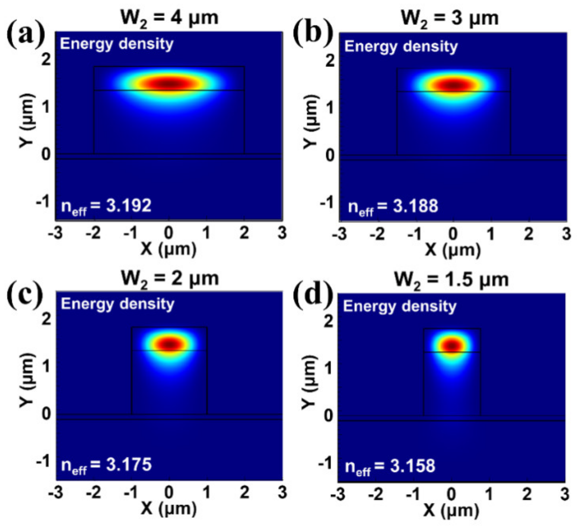
The 2D mode profiles with W2 = 4 μm, W2 = 3 μm, W2 = 2 μm, and W2 = 1.5 μm and their respective propagating indices are shown in Figure 10a–d, respectively. These were simulated with polymer as the upper cladding and material at both sides of the waveguide. Our simulation showed that at W2 = 1.5 μm, the mode began to be coupled to the substrate at the passive waveguide device as the real part of its propagating refractive index (n = 3.158) became lower than the refractive index of the InP lower cladding (n = 3.17), and in fact, the imaginary part of its propagating refractive index had a high nonzero value when the absorbing boundary was used for boundary lines surrounding the substrate, indicating energy loss through the substrate.
Thus, from the above data, we can conclude that it is possible to use a W2 narrower than 4 μm but wider than (or equal to) 2 μm to achieve roughly the same mode connection efficiency but with a taper length a few times shorter for both LBT and LT than that of the 4-μm wide case. These analyses also show that the device structures were reasonably tolerant to structural and fabrication variations in terms of impacting the device performances.

3. Conclusions

In summary, we analyzed an integration platform capable of realizing the integration of active or passive InP-based photonic devices without the use of material regrowth. The method makes use of the transparent intrinsic layer of the gain waveguide core as a passive waveguide and an adiabatic mode connection structure to bring the optical beam from the passive waveguide into the active gain waveguide region, somewhat similar to the approach used in heterogenous integration of InP devices on silicon involving evanescent interaction of the beam with the active gain medium on top. The optimal structural parameters for the fiber-coupling surface grating structure was simulated and given. The fiber beam-coupling efficiency of this surface grating was found to be 88.3% when a gold reflector was placed below the grating region. The optical gain achievable for the active waveguide device section with MQW was found to be ~20 dB/mm with the use of a 560-nm thick waveguide and 3 quantum wells. With use of a thinner waveguide core thickness of 410 nm, a gain of over 24 dB/mm was achievable, but the upper cladding of the passive waveguide region would have to have a higher refractive index. The photonic device integration method introduced here is suitable for realizing compact InP-based photonic integrated circuits with both active and passive photonic devices integrated together without the use of material regrowth. Like all other photonic integration schemes, this scheme also has its advantages and disadvantages. This scheme is relatively simple in terms of connecting the passive and active sections together, as the mode connection efficiency is not very sensitive to the length or shape of the taper or possible fabrication inaccuracies. The performance of the taper is also not wavelength-sensitive, which is the nature of an “adiabatic taper” (compared with resonance waveguide coupling). The mode connection is along a main waveguide core (not between two separate waveguides, such as in the case of the vertical twin-waveguide method), making it able to achieve high coupling efficiency (>99%) with a relatively short taper length, which is high compared with the typical passive section to active section coupling efficiency of ~95% for the twin-waveguide method. The passive-active waveguide joint would be smoother than most regrowth methods. A disadvantage of this scheme is that it is not easy to involve two or more different active structures (e.g., a laser and modulator), though in principle, one can grow different active structures on top of the main waveguide core via selective area growth.
For example, the scheme introduced here can be applied in various situations, including but not limited to the realization of Distributed Bragg Refractor (DBR) lasers, for which the laser cavity is formed by two linear Bragg grating structures that can be fabricated in the passive device sections (Section B and Sections F), and the active gain section (Section D) is between Section B and Section F to provide the intra-cavity optical gain. Likewise, it can be used to realize a diffraction grating-based laser [20,21,22,23], for which the integrated diffraction grating is fabricated in the passive device section (e.g., Section F) to provide backside frequency selective reflection, and a linear Bragg grating structure at the “front” is fabricated in the passive device section of Section B to serve as the “laser output mirror” to output the laser beam to the surface grating structure of Section A, which then couples the output beam into an optical fiber. Other applications include integrated devices involving semiconductor optical amplifiers (SOAs), such as ultra-fast all-optical switches [24,25,26], for which the two Y-splitters (or the MMI splitter or 2 × 2 optical waveguide coupler splitter) needed for forming a Mach Zehnder interferometer can be fabricated in the passive device sections (Sections B and F). The passive sections can also form thermo-optic-based devices (similar to thermo-optic switching devices implemented using silicon waveguides). The passive section can also be implanted with lateral P-N junctions to realize electro-optic-type modulators (similar to a silicon modulator). This will enable integration of a laser with a modulator on the chip. These are some of the potential applications among many other possible applications. The advantage over the twin-waveguide method was already discussed above. The advantage over the QWI method would be lower loss and broader optical bandwidth. (QWI usually can only shift the passive sections to transparency for a narrow optical bandwidth of ~50 nm) The advantage over the regrowth method would be lower fabrication complexity and lower fabrication cost for the integrated device examples discussed.
To summarize, the photonic integration platform described here is referred to as adiabatic active-layer waveguide connection (ALWC)-based active-passive photonic device integration method, or simply the “ALWC Photonic Integration Method”. It will have various applications that can make use of its advantages and can complement other photonic device integration methods in its areas of applicability.

Author Contributions

Conceptualization, C.C.; formal analysis, J.L.; data curation, C.W. and J.L.; methodology, Y.H. and C.C.; funding acquisition, S.-T.H. and D.Z.; project administration, S.-T.H.; resources, Z.S. and Z.C.; writing—original draft, F.Y. and C.W.; writing—review and editing, J.L. and C.C. All authors have read and agreed to the published version of the manuscript.

Funding

This research was funded by the National Key R&D Program of China (2019YFB2203001), Science and Technology Development Plan of Jilin Province (20190302010GX), and National Natural Science Foundation of China (61675087, 61875069, 11774112 and 11604110). This work was partially supported by a NASA Early Stage Innovations grant. This work was also performed, in part, at the Center for Nanoscale Materials and a U.S. Department of Energy Office of Science user facility and was supported by the U.S. Department of Energy’s Office of Science under Contract No. DE-AC02-06CH11357.

Institutional Review Board Statement

Not applicable.

Informed Consent Statement

Not applicable.

Data Availability Statement

Not applicable.

Conflicts of Interest

The authors declare no conflict of interest.

References

  1. Midkiff, J.; Yoo, K.M.; Shin, J.; Dalir, H.; Teimourpour, M.; Chen, R.T. Optical phased array beam steering in the mid-infrared on an InP-based platform. Optica 2020, 7, 1544–1547. [Google Scholar] [CrossRef]
  2. Augustin, L.M.; Santos, R.; Haan, E.; Kleijn, S.; Thijs, P.J.A.; Latkowski, S.; Zhao, D.; Yao, W.; Bolk, J.; Ambrosius, H.; et al. InP-Based Generic Foundry Platform for Photonic Integrated Circuits. IEEE J. Sel. Top. Quantum Electron. 2018, 24, 6100210. [Google Scholar] [CrossRef]
  3. Soares, F.M.; Baier, M.; Gaertner, T.; Feyer, M.; Möhrle, M.; Grote, N.; Schell, M. High-Performance InP PIC Technology Development based on a Generic Photonic Integration Foundry. In Proceedings of the Optical Fiber Communication Conference, Optical Society of America, San Diego, CA, USA, 11–15 March 2018. [Google Scholar]
  4. Spencer, D.T.; Drake, T.; Briles, T.C.; Stone, J.; Sinclair, L.C.; Fredrick, C.; Li, Q.; Westly, D.; Ilic, B.R.; Bluestone, A.; et al. An optical-frequency synthesizer using integrated photonics. Nature 2018, 557, 81–85. [Google Scholar] [CrossRef]
  5. Williams, K.A.; Bente, E.A.J.M.; Heiss, D.; Jiao, Y.; Ławniczuk, K.; Leijtens, X.J.M.; van der Tol, J.J.G.M.; Smit, M.K. InP photonic circuits using generic integration. Photon. Res. 2015, 3, B60–B68. [Google Scholar] [CrossRef]
  6. Chen, Z.-B.; Cai, J.; Ji, X.; Sun, Y.; Lin, J.; Zhao, X.; Yu, X.; Zhang, J.; Chao, F.-S. On the growth and fabrication of an integrated DFB laser and EA modulator. In Application of Photonic Technology 6; Lessard, R.A., Lampropoulos, G.A., Eds.; International Society for Optics and Photonics: Bellingham, DC, USA, 2003. [Google Scholar]
  7. Studenkov, P.V.; Gokhale, M.R.; Wei, J.; Lin, W.; Glesk, I.; Prucnal, P.R.; Forrest, S.R. Monolithic integration of an all-optical Mach Zehnder demultiplexer using an asymmetric twin-waveguide structure. IEEE Photon. Technol. Lett. 2001, 13, 600–602. [Google Scholar] [CrossRef]
  8. Jain, S.R.; Sysak, M.N.; Kurczveil, G.; Bower, J.E. Integrated hybrid silicon DFB laser-EAM array using quantum well intermixing. Opt. Express 2011, 19, 13692–13699. [Google Scholar] [CrossRef] [PubMed] [Green Version]
  9. Fujii, T.; Takeda, K.; Nishi, H.; Diamantopoulos, N.; Sato, T.; Kakitsuka, T.; Tsuchizawa, T.; Matsuo, S. Multiwavelength membrane laser array using selective area growth on directly bonded InP on SiO2/Si. Optica 2020, 7, 38–846. [Google Scholar] [CrossRef]
  10. Zhang, J.; Muliuk, G.; Juvert, J.; Kumari, S.; Goyvaerts, J.; Haq, B.; Beeck, C.; Kuyken, B.; Morthier, G.; Thourhout, D.; et al. III-V-on-Si photonic integrated circuits realized using micro-transfer-printing. APL Photon. 2019, 4, 110803. [Google Scholar] [CrossRef] [Green Version]
  11. Davenport, M.L.; Skendzic, S.; Volet, N.; Hulme, J.C.; Heck, M.J.R.; Bowers, J.E. Heterogeneous Silicon/III-V Semiconductor Optical Amplifiers. IEEE J. Sel. Top. Quantum Electron. 2016, 22, 78–88. [Google Scholar] [CrossRef]
  12. Yu, J.; Yamada, H. Design and investigation of a dual-layer grating coupler for efficient vertical fiber-chip coupling. Appl. Phys. Express 2019, 12, 012004. [Google Scholar] [CrossRef]
  13. Mekis, A.; Gloeckner, S.; Masini, G.; Narasimha, A.; Pinguet, T.; Sahni, S.; Dobbelaere, P. A Grating-Coupler-Enabled CMOS Photonics Platform. IEEE J. Sel. Top. Quantum Electron. 2011, 17, 597–607. [Google Scholar] [CrossRef]
  14. Laere, F.; Roelkens, G.; Ayre, M.; Schrauwen, J.; Taillaert, D.; Thourhout, D.; Krauss, T.F.; Baets, R. Compact and Highly Efficient Grating Couplers Between Optical Fiber and Nanophotonic Waveguides. J. Lightwave Technol. 2007, 25, 151–156. [Google Scholar] [CrossRef] [Green Version]
  15. Mu, J.F.; Sefunc, M.A.; Xu, B.J.; Garcia-Blanco, S.M. Design and fabrication of adiabatic vertical couplers for hybrid integration by flip-chip bonding. Proc. SPIE 2016, 9750, 975012. [Google Scholar]
  16. Wang, L.; Bogaerts, W.; Dumon, P.; Baets, R.; Morthier, G. Athermal arrayed waveguide gratings in silicon-on-insulator by overlaying a polymer cladding on narrowed arrayed waveguides. Appl. Opt. 2012, 51, 1251–1256. [Google Scholar] [CrossRef] [Green Version]
  17. Cai, Z.; Zhang, Y.; Song, Y.; Cheng, Q.; Zheng, Y.; Cui, Z.; Shi, Z.; Chen, C.; Zhang, D. Optically transparent fluorine-containing polycarbonates with high refractive indices for thermo-optic switches. Mater. Chem. Front. 2017, 1, 2031–2038. [Google Scholar] [CrossRef]
  18. Zheng, Y.; Chen, C.; Wang, J.; Shi, Z.; Cai, Z.; Sun, X.; Wang, F.; Cui, Z.; Zhang, D. Fluorinated photopolymer waveguide thermooptic switches with loss-compensation function based on erbium-containing cladding structure. Phys. Chem. Chem. Phys. 2016, 18, 25553–25559. [Google Scholar] [CrossRef]
  19. Namnabat, S.; Kim, K.; Jones, A.; Himmelhuber, R.; Derose, C.T.; Trotter, D.C.; Starbuck, A.L.; Pomerene, A.; Lentine, A.L.; Norwood, R.A. Athermal silicon optical add-drop multiplexers based on thermo-optic coefficient tuning of sol-gel material. Opt. Express 2017, 25, 21471–21482. [Google Scholar] [CrossRef] [Green Version]
  20. Wang, Y.; Engelen, J.; Reniers, S.F.G.; Rijn, M.; Zhang, X.; Cao, Z.; Dolores-Calzadilla, V.; Williams, K.A.; Smit, M.K.; Jiao, Y. InP-Based Grating Antennas for High-Resolution Optical Beam Steering. IEEE J. Sel. Top. Quantum Electron. 2021, 27, 6100107. [Google Scholar] [CrossRef]
  21. He, W.; Zhang, Q.; Meng, F.; Zhu, L. Single-wavelength tunable erbium-doped fiber laser based on electron beam lithography inscribed varied-period plane diffraction grating. Opt. Laser Technol. 2021, 140, 107064. [Google Scholar]
  22. Belay, G.Y.; Hoving, W.; Put, A.; Vervaeke, M.; VanErps, J.; Thienpont, H.; Ottevaere, H. Miniaturized broadband spectrometer based on a three-segment diffraction grating for spectral tissue sensing. Opt. Laser Eng. 2020, 134, 106157. [Google Scholar] [CrossRef]
  23. Wang, Y.; Wei, Y.; Huang, Y.; Tu, Y.; Ng, D.; Lee, C.; Zheng, Y.; Liu, B.; Ho, S.T. Silicon/III-V Laser with Super-compact diffraction grating for WDM applications in electronic-photonic integrated circuits. Opt. Express 2011, 19, 2006–2013. [Google Scholar] [CrossRef] [PubMed]
  24. Gao, J.; Nazemosadat, E.; Yang, Y.; Fu, S.; Tang, M.; Schröder, J.; Karlsson, M.; Andrekson, P.A. Elliptical-Core Highly Nonlinear Few-Mode Fiber Based OXC for WDM-MDM Networks. IEEE J. Sel. Top. Quantum Electron. 2021, 27, 7600511. [Google Scholar] [CrossRef]
  25. Grinblat, G.; Zhang, H.; Nielsen, M.P.; Krivitsky, L.; Berté, R.; Li, Y.; Tilmann, B.; Cortés, E.; Oulton, R.F.; Kuznetsov, A.I.; et al. Efficient ultrafast all-optical modulation in a nonlinear crystalline gallium phosphide nanodisk at the anapole excitation. Sci. Adv. 2020, 6, eabb3123. [Google Scholar] [CrossRef]
  26. Liu, W.; Li, M.; Guzzon, R.S.; Norberg, E.J.; Parker, J.S.; Lu, M.; Coldern, L.A.; Yao, J. A fully reconfigurable photonic integrated signal processor. Nat. Photonics 2016, 10, 190–196. [Google Scholar] [CrossRef]
Figure 1. (a) The geometry of the proposed photonic device integration scheme with 4 separate sections. (b) X-Z cross-sectional profile of the 4 sections.
Photonics 08 00433 g001
Figure 2. (a) Y-Z cross-sectional diagram of the vertical beam fiber-coupling apodized grating with a gold reflecting mirror structure below the grating. (b) Y-X cross-sectional diagram of the InGaAs/InGaAsP MQW active waveguide device.
Photonics 08 00433 g002
Figure 3. (a) The schematic and computational model for the vertical beam fiber-coupling apodized InGaAsP grating and (b) the optical field distribution between the optical fiber and grating, simulated by Lumerical 2D FDTD software.
Photonics 08 00433 g003
Figure 4. (a) The relationship between the vertical beam fiber coupling efficiency and the thickness of the bottom polymer cladding. (b) The normalized beam intensity profile (Igra) for the beam from the grating based on an FDTD simulation, the Gaussian function fitting curve (Igfi) for the beam profile Igra, and the normalized beam intensity profile (Ifib) of the fiber’s fundamental mode. (c) The relationship between the fiber angle and the coupling efficiency (with the wavelength at 1550 nm). (d) The coupling efficiency as a function of the optical wavelength. showing a bandwidth of 44.3 nm at −1.5 dB (reduced from the peak by 30%) with θ = 10°.
Photonics 08 00433 g004
Figure 5. (a) The mode connection efficiency between the 15-μm wide waveguide and the 4-μm wide waveguide as a function of the taper length L3. The taper loss at L3 = 240 μm was 1.5%. (b) Simulated 2D profile of the input mode. (c) Simulated 2D profile of the output mode. (d) Horizontal cross-section illustrating the behavior of the propagating beam in the taper with L3 = 240 μm.
Photonics 08 00433 g005
Figure 6. (a) The mode connection efficiency for the bottom taper in the passive waveguide device as a function of the taper length LBT. (b) Simulated 2D profile of the input mode. (c) Simulated 2D profile of the output mode. (d) Horizontal cross-section illustrating the behavior of the propagating beam in the taper with LBT = 162 μm. (e) Vertical cross-section illustrating the behavior of the propagating beam in the taper with LBT = 162 μm. (f) Slanted opening to fabricate the InP taper.
Photonics 08 00433 g006
Figure 7. (a) The mode connection efficiency for the top taper in the active waveguide device as a function of the taper length LT. (b) Simulated 2D profile of the input mode. (c) Simulated 2D profile of the output mode. (d) Horizontal cross-section illustrating the behavior of the propagating beam in the taper with LT = 114 μm. (e) Vertical cross-section illustrating the behavior of the propagating beam in the taper with LT = 114 μm.
Photonics 08 00433 g007
Figure 8. (a) Vertical FWHM mode size in the 4-μm wide output region of the passive waveguide device as a function of the InGaAsP layer thickness with polymer (n = 1.5) as the top cladding and InP as the bottom cladding. (b) The 2D mode intensity profile for a core thickness of 350 nm. (c) The 2D mode intensity profile for a core thickness of 400 nm. (d) The 2D mode intensity profile for a core thickness of 500 nm. (e) Vertical FWHM mode size in the 4-μm wide output region of the passive waveguide device as a function of the InGaAsP layer thickness with TiO2 (n = 2.43) as the top cladding and InP as the bottom cladding. (f) The 2D mode intensity profile for a core thickness of 325 nm (for the TiO2 case). (g) The 2D mode intensity profile for a core thickness of 350 nm (for the TiO2 case). (h) The 2D mode intensity profile for a core thickness of 400 nm (for the TiO2 case).
Photonics 08 00433 g008
Figure 9. (a) Mode connection efficiency for the grating output region as a function of L3 for the case of W2 = 3 μm. (b) Mode connection efficiency for the grating output region as a function of L3 for the case of W2 = 2 μm. (c) Mode connection efficiency for the passive waveguide device as a function of LBT for the case of W2 = 3 μm. (d) Mode connection efficiency for the passive waveguide device part as a function of LBT for the case of W2 = 2 μm. (e) Mode connection efficiency for the active-passive waveguide connection as a function of LT for the case of W2 = 3 μm. (f) Mode connection efficiency for the active-passive waveguide connection as a function of LT for the case of W2 = 2 μm.
Photonics 08 00433 g009
Figure 10. (a) The 2D mode profile with W2 = 4 μm. (b) The 2D mode profile with W2 = 3 μm. (c) The 2D mode profile with W2 = 2 μm. (d) The 2D mode profile with W2 = 1.5 μm.
Photonics 08 00433 g010
Table 1. Detailed parameters for each semiconductor layer of the MQW waveguide amplifier (the bandgap of InGaAsP is at 1.25 μm).
Layer DefinitionTypeThickness (nm)MaterialRefractive IndexCarrier Concentration (cm−3)
P-contactP100InGaAs3.461 × 1019
P-claddingP1500InP3.171 × 1018
Barrier layerI10InGaAsP3.31
Well layerI10InGaAs3.46
Barrier layerI10InGaAsP3.31
Well layerI10InGaAs3.46
Barrier layerI10InGaAsP3.31
Well layerI10InGaAs3.46
Barrier layerI500InGaAsP3.31
N-claddingN1350InP3.171 × 1018
Etch-stop layerN25InGaAsP3.311 × 1018
N-doped substrateNSubstrateInP3.311 × 1018
Table 2. Specific values of Gi and Di for each grating period (Λi = Gi + Di).
IGi (nm)Di (nm)iGi (nm)Di (nm)iGi (nm)Di (nm)
126.8447.01278.3406.423233.5283.8
226.8447.01388.7398.224233.5283.8
326.8447.014100.1389.225233.5283.8
426.8447.015112.5379.426233.5283.8
526.8447.016126.1368.627233.5283.8
632.1442.917141.3356.728233.5283.8
738.0438.218158.3343.329233.5283.8
844.6433.019178.2327.730233.5283.8
951.9427.220201.8308.831233.5283.8
1059.9420.921233.5283.832233.5283.8
1168.7414.022233.5283.833233.5283.8
Table 3. Parameters used for the MQW active waveguide section.
ParameterValue
Width of active quantum-well waveguide (nm)4000
Thickness of active quantum-well waveguide core (nm)560
Effective refractive index of active waveguide3.362
Recommended length of top taper waveguide (LT) (μm)114
Quantum well/barrier materialIn0.53Ga0.47As (Q = 1.7 μm)/InGaAsP (Q = 1.25 μm)
Number of quantum wells3
Thickness of a single quantum well (nm)10
Mode overlapping factor with quantum well3.0%
Estimated optical gain of active waveguide~20 dB/mm
Table 4. Exemplary length for each section and the estimated optical loss at each section.
Section LabelSection ASection BSection CSection D
TypePassivePassivePassiveActive
LengthL1 = 20 μm
(h3 = 1.25 μm)
L3 = 240 μmLBT = 162 μmLT = 114 μmL6
Efficiency88.3%98.5%97.1%99.0%\
Loss−0.54 dB−0.066 dB−0.13 dB−0.044 dB\
Gain\\\\+19.5 dB/mm
Publisher’s Note: MDPI stays neutral with regard to jurisdictional claims in published maps and institutional affiliations.

