Letter

Silicon Photonic Mode-Division Reconfigurable Optical Add/Drop Multiplexers with Mode-Selective Integrated MEMS Switches

School of Electrical Engineering and Computer Science, Gwangju Institute of Science and Technology, Buk-gu, Gwangju 61005, Korea
*
Author to whom correspondence should be addressed.
Photonics 2020, 7(4), 80; https://doi.org/10.3390/photonics7040080
Submission received: 4 August 2020 / Revised: 18 September 2020 / Accepted: 22 September 2020 / Published: 24 September 2020
(This article belongs to the Special Issue Photonic Devices and Systems)

Abstract

:
Mode-division multiplexing (MDM) is an attractive solution for future on-chip networks to enhance the optical transmission capacity with a single laser source. A mode-division reconfigurable optical add/drop multiplexer (ROADM) is one of the key components to construct flexible and complex on-chip optical networks for MDM systems. In this paper, we report on a novel scheme of mode-division ROADM with mode-selective silicon photonic MEMS (micro-electromechanical system) switches. With this ROADM device, data carried by any mode-channels can be rerouted or switched at an MDM network node, i.e., any mode could be added/dropped to/from the multimode bus waveguide flexibly and selectively. Particularly, the design and simulation of adiabatic vertical couplers for three quasi-TE modes (TE0, TE1, and TE2 modes) based on effective index analysis and mode overlap calculation method are reported. The calculated insertion losses are less than 0.08 dB, 0.19 dB, and 0.03 dB for the TE0 mode, TE1 mode, and TE2 mode couplers, respectively, over a wavelength range of 75 nm (1515–1590 nm). The crosstalks are below −20 dB over the bandwidth. The proposed device is promising for future on-chip optical networks with flexible functionality and large-scale integration.

1. Introduction

The explosive growth of data traffic passing through optical networks has emerged as a critical problem in optical communications [1]. The demand for high capacity and flexible data transmission has become increasingly challenging. High density, low power consumption, low-cost, remotely configurable devices based on monolithic photonic integration circuits are required for the next generation optical networks [2,3]. The capacity of optical interconnects was enhanced by utilizing advanced multiplexing techniques enabling parallel multi-channel transmissions. Wavelength-division multiplexing (WDM) was introduced as a breakthrough to provide high capacity data communications by allowing simultaneous transmissions of multiple wavelength channels in a single optical fiber [4,5]. Polarization-division-multiplexing (PDM) is another well-established technique to double the capacity with two polarized channels [6]. Recently, mode-division multiplexing (MDM) has emerged as a potential route to increase the data transmission capacity by utilizing the multiple spatial guided-modes in multimode waveguides, which can enhance the optical link capacity many folds using only a single wavelength source [7]. MDM appears particularly attractive for future networks-on-chip in computing because it does not require an array of lasers of precise wavelengths like WDM systems do. Hybrid multiplexing techniques, such as MDM-WDM [8,9,10] and MDM-PDM [11], have been also realized. MDM communications were demonstrated with multiple modes in silicon photonic integrated circuits, where each mode represented an independent data channel [12,13,14,15,16,17,18,19,20,21,22]. On-chip MDMs have been realized by various structures, such as multimode interferometers (MMIs) [14,15], asymmetric directional couplers (ADCs) [16,17], topology optimized waveguides [18,19], and adiabatic mode-evolution couplers [20,21,22].
Mode-selective switches (MSSs) and mode-division reconfigurable optical add/drop multiplexers (ROADMs) are key building blocks to construct on-chip MDM networks, which allow each mode channel to be transmitted, rerouted, dropped, or added to perform optical channel processing. Typical MSSs and mode-division ROADMs are realized with combined architectures of passive mode-division (de)multiplexers and space switches [23,24,25,26,27,28,29,30] or cascaded mode-selective ring resonators with bus waveguide taper transitions [31,32,33] that are subject to accumulated optical losses and crosstalks with large footprints owing to the requirement for combining various photonic components. In this paper, we propose a novel scheme for mode-division ROADMs with mode-selective silicon photonic MEMS switches. The mode-selective silicon photonic MEMS switches allow direct and selective mode-couplings from the bus waveguide, eliminating the requirement of mode-division (de)multiplexers or taper transitions in the bus waveguide. The proposed ROADM device is composed of vertically-actuated adiabatic couplers for the three quasi-TE modes (i.e., TE0, TE1, and TE2 modes), which inherit the advantages of silicon photonic MEMS switches such as unprecedented loss, crosstalk, and extinction ratio [25,34,35]. The modes in our rib waveguide are quasi-TE modes with dominant electric field component [36]. However, we will call them just TE modes for convenience as common terminology in silicon photonics. The total length for three couplers is short (less than 300 µm) and the device exhibits low insertion losses less than 0.08 dB for TE0 mode coupler, less than 0.19 dB for TE1 mode coupler, less than 0.03 dB for TE2 mode coupler over a wide bandwidth of 75 nm.

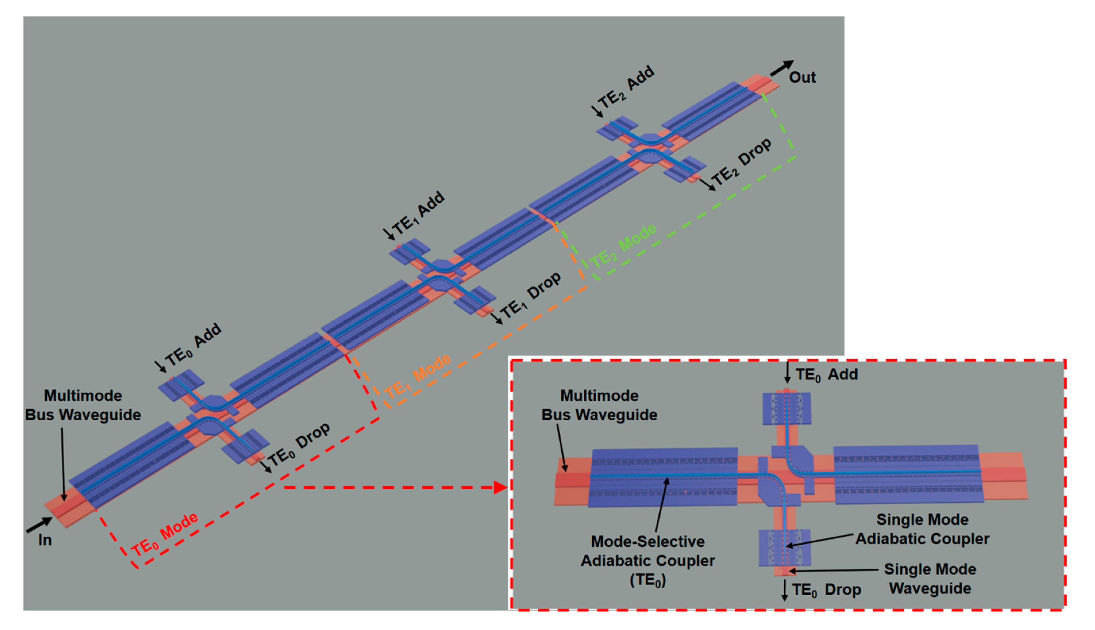
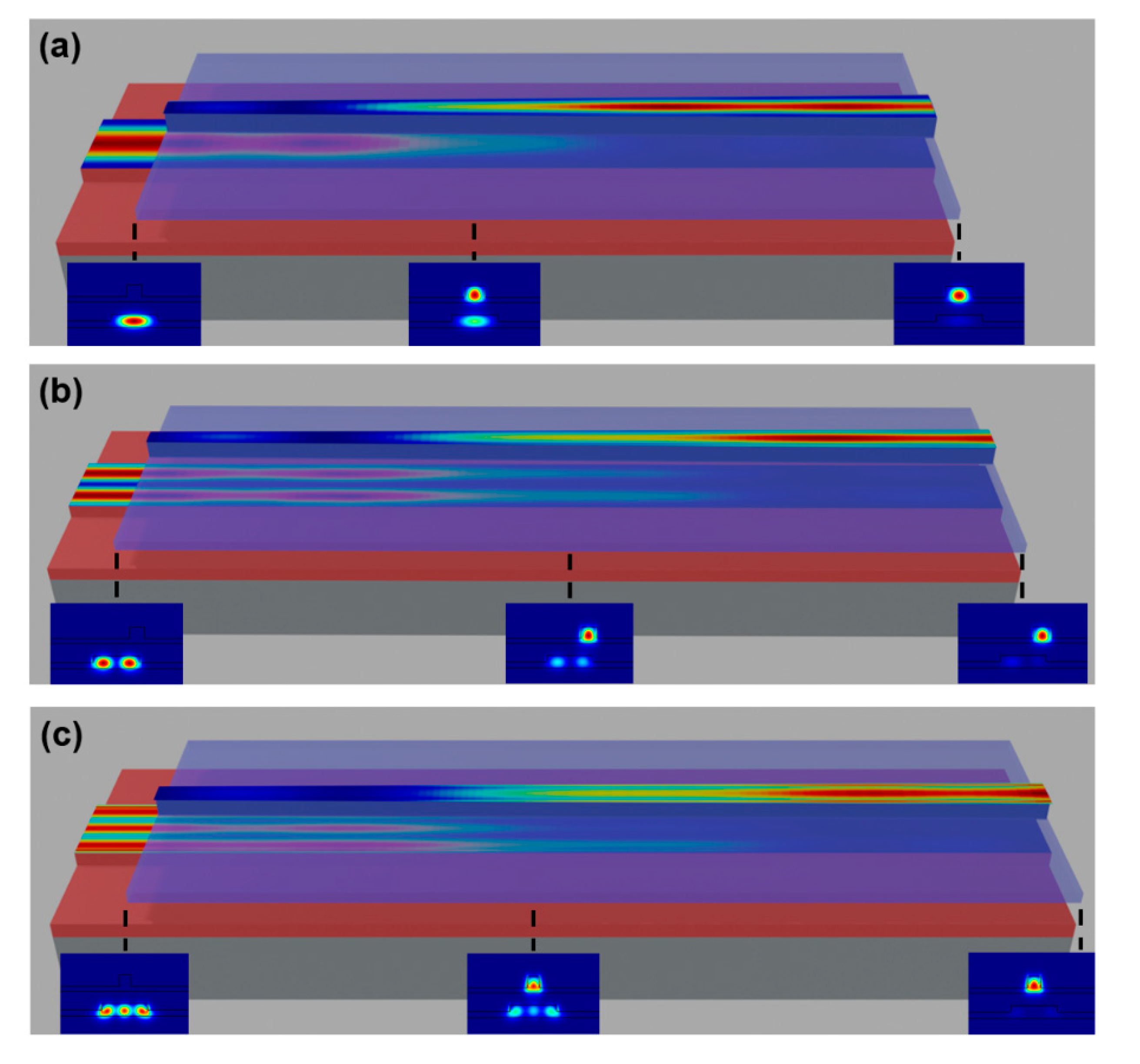
2. Device Architecture

The device architecture is based on mode-selective MEMS-actuated vertical adiabatic couplers as shown in Figure 1. The device was designed for operation with TE-polarization. The multimode bus waveguide (red) was implemented with a 2-µm-thick buried oxide (BOX) layer (n = 1.444 at 1550 nm) and a silicon rib waveguide (n = 3.476 at 1550 nm) with a height of 220 nm, a partial etch depth of 110 nm, and a constant width of 1.4 μm as shown in Figure 2. The bus waveguide had a fixed width, which was important to sustain system modularity. The multimode bus rib waveguide with a constant width of 1.4 μm supported three first TE modes only, i.e., TE0, TE1, and TE2 modes. The upper adiabatically-tapered waveguide (shown in light blue for highlight purpose; the material is poly-Si (n = 3.476 at 1550 nm), which is similar to the MEMS structure (shown in blue)) was 200 nm shallow-etched (300 nm-height) poly-Si rib waveguide. Any of the mode channels (TE0, TE1, and TE2 mode channels) could be added/dropped to/from the bus waveguide by turning on the MEMS-actuation and achieving the optimum gap spacing with the mechanical stoppers [25,34,35]. The add/drop ports were designed with single mode waveguides and typical single mode MEMS switches, which were experimentally demonstrated in [25]. It is clearly noted that for add/drop ports, the bus waveguides are single mode waveguide with width of 600 nm. By controlling the MEMS-actuators of a target mode channel, the mode channel can be coupled out from the bus waveguide and dropped to the single mode waveguide in the targeted drop port. Similarly, a new channel signal can be added from an add port and coupled into the bus waveguide. The MEMS actuators were designed with parallel-plated-type gap-closing electrostatic actuators with folded spring suspensions as reported in previous works [25,34,35]. The fabrication process including MEMS structure implementation was similar to the details presented in those works. In our device, the ON state occurred when the gap spacing was 250 nm, which was precisely defined by the mechanical stoppers. The gap spacing of 1000 nm (the rest-position of the actuator) defined the OFF state. The estimated switching time between ON state and OFF state should be in the range of sub-microsecond as experimentally reported in [25,34,35].

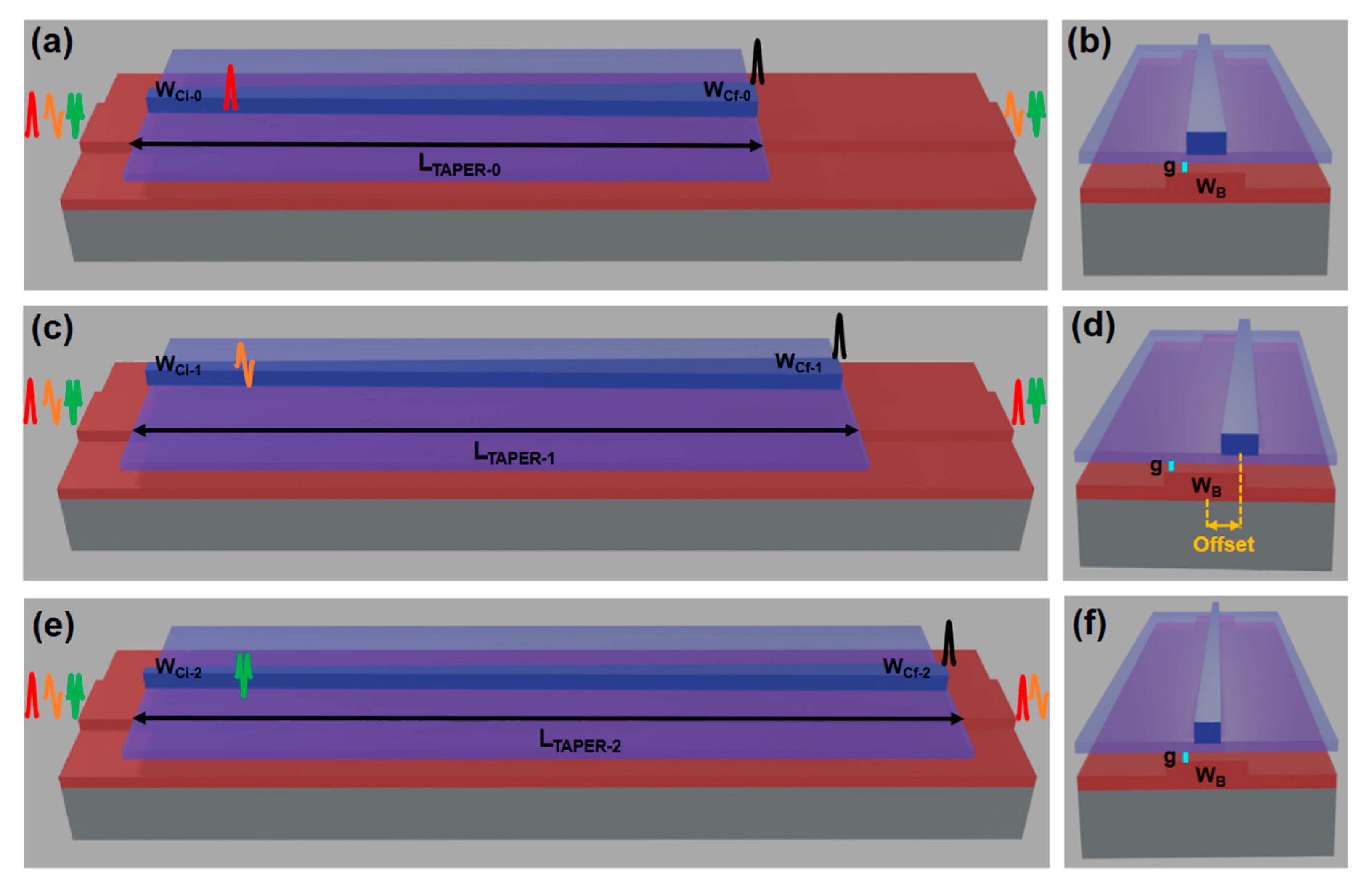
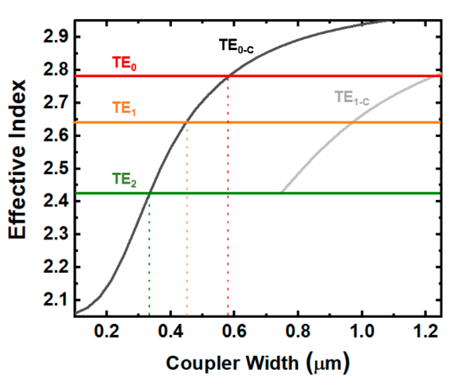
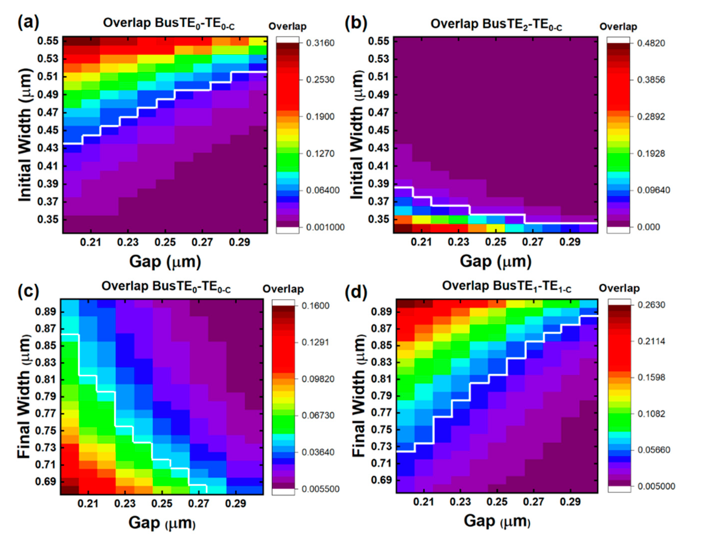
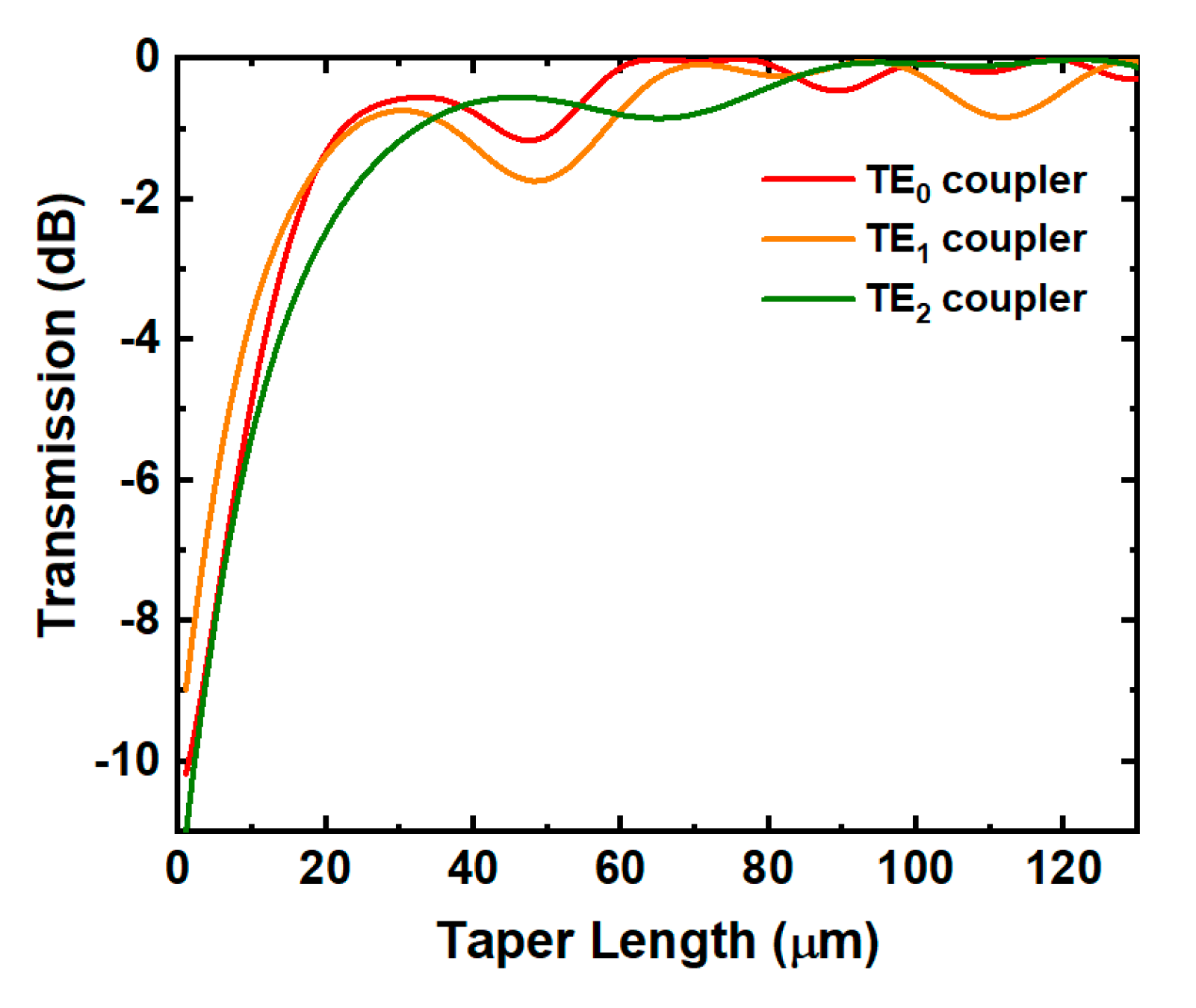
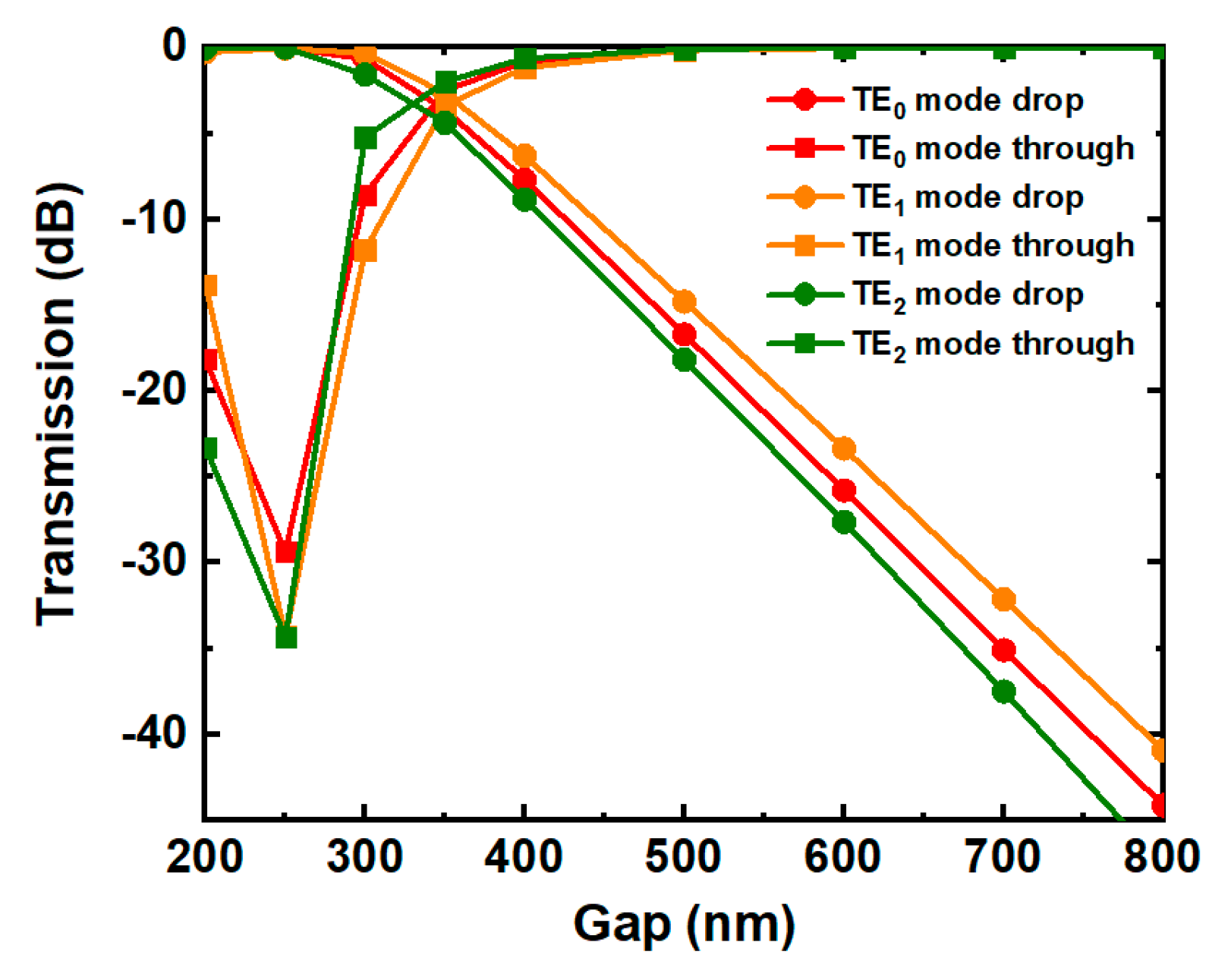
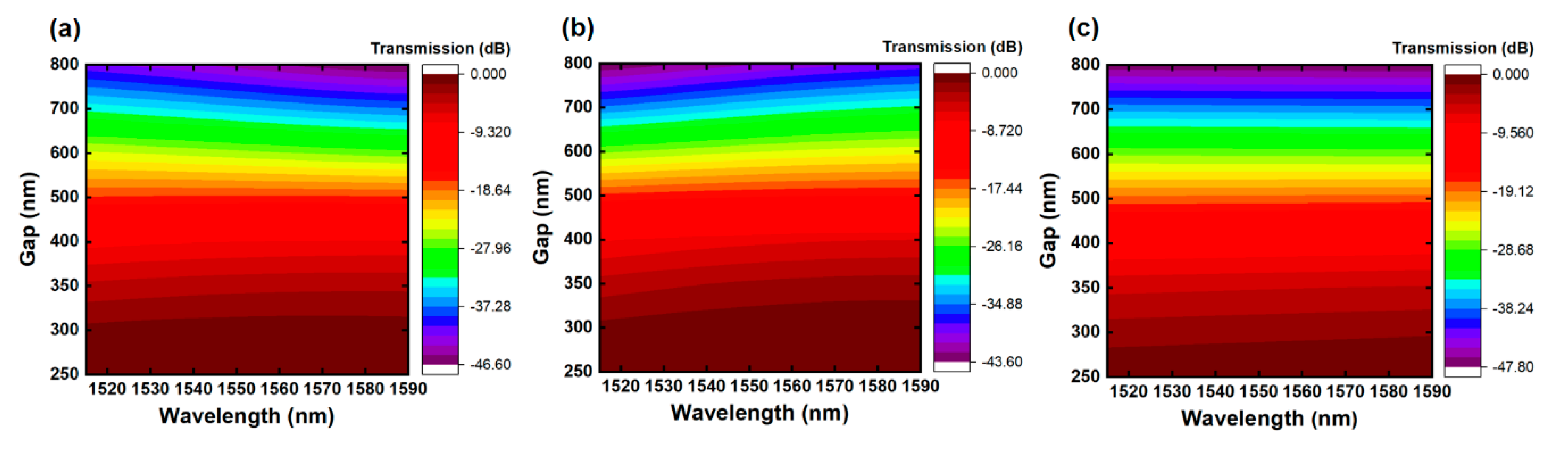
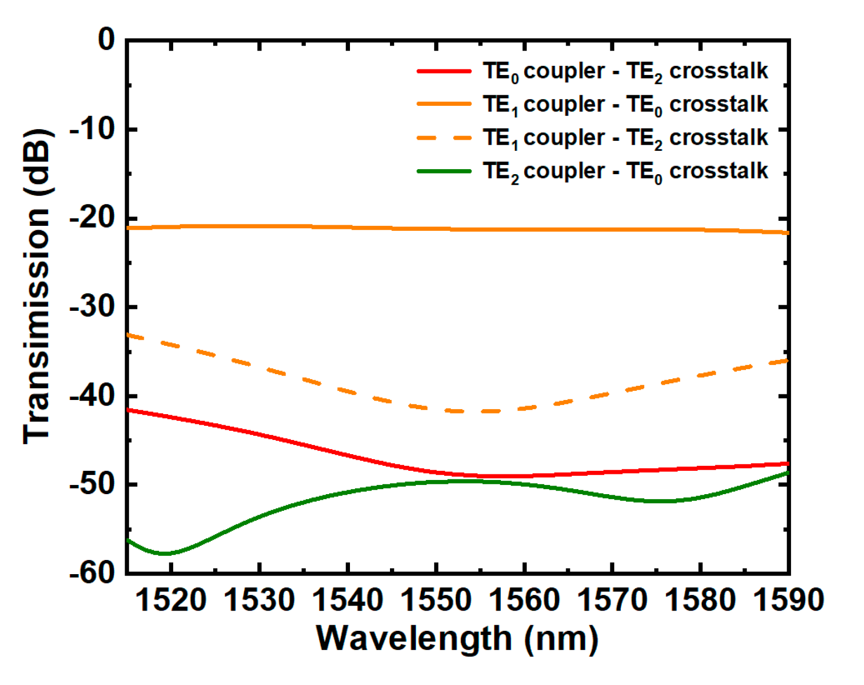
3. Device Design and Simulation Results

A basic building block of the mode-division ROADM with integrated MEMS switching was a mode-selective adiabatic vertical coupler, which could add/drop a signal to/from the selected mode of the multimode waveguide serving as an optical data bus. The schematics of the simplified mode-selective adiabatic vertical couplers are shown in Figure 2. In the real simulation, the structure includes the vertical S-bending and straight output waveguide, which results in very small propagation loss and almost no affection to the coupling. It was designed based on adiabatic power transfer, which characterized a linearly changing coupling coefficient along the propagation length. Perspective views of the TE0 mode coupler in are presented in Figure 2a,b. Those of the TE1 mode coupler and TE2 mode coupler are presented in Figure 2c,d and in Figure 2e,f, respectively. The multimode bus waveguide of a constant width (WB = 1.4 µm) supports three TE-polarized modes of TE0, TE1, and TE2. WCi-j, WCf-j, and LTAPER-j are the initial width, final width and the length of the tapered coupler waveguides, respectively (j is 0, 1, 2 in accordance with the modes of TE0, TE1, and TE2); g is the vertical gap between the bus waveguide and the coupler waveguide. The vertical couplers for the TE0 mode and TE2 mode were laterally aligned at the center of the bus waveguide since their mode profiles exhibited even symmetries, which provided good spatial mode overlapping with the TE0 mode of the coupler waveguide. For the TE1 mode coupler, it was required to have a lateral offset from the center of bus waveguide as shown in Figure 2d to achieve spatial mode matching as the mode profile of the TE1 mode had odd symmetry.
The couplers were designed by first analyzing the effective index matching as shown in Figure 3. The effective indices of the bus waveguide were matched at the coupler widths of 0.58 µm, 0.45 µm, and 0.33 µm for the TE0 mode, TE1 mode, and TE2 mode, respectively. The width of the each coupler waveguide should be tapered adiabatically from an initial width (below the corresponding matched width) to a final width (above the corresponding matched width). The black curve, which represented the effective index of fundamental mode in the coupler waveguide, was for defining the matching points with the modes (TE0, TE1, TE2 mode) in the bus waveguide. Then, we could define the designed space for initial width and final width for each coupler waveguide. The first order mode (shown in light grey) was for limiting the final width of TE0 mode’s coupler waveguide, which should be far smaller from the matching width for effective indices of TE1 in the bus waveguide and TE1-C in the coupler waveguide. Moreover, the initial width and the final width should be designed not to cause unwanted-mode scatterings for ideal adiabatic operation. Therefore, we investigated mode overlap integrals between the individual bus waveguide and the coupled system of the bus and coupler waveguides. The results of the mode overlap integrals of the taper initial and final widths for the TE0 mode coupler are shown in Figure 4. We designed the initial and final widths to have overlap integrals below 0.05 to suppress unwanted mode scatterings at the beginning and the end of the tapered coupler. The gap of 250 nm was chosen in order to keep the tapered length short with low overlap integrals. The initial and final widths of the taper was designed to be 450 nm and 770 nm, respectively. For the TE1 mode coupler, the lateral offset was optimized to be 600 nm with a strong coupling between the target super modes (TE1-like mode in the bus waveguide and TE0-like mode in the coupler waveguide, see Figure S1 in Supplementary Information). Subsequently, the initial width and final width were designed to be 400 nm and 500 nm for the TE1 mode coupler from the mode overlap analysis. Similarly, the initial and final widths of the TE2 mode coupler were designed to be 310 nm and 360 nm, respectively (see Figures S2 and S3 in Supplementary Information).
Using eigenmode expansion (EME) solver (Lumerical Mode Solution), the taper lengths for the three couplers were determined by investigating the transmission with the taper length sweep as shown in Figure 5. It is noted that we did the convergence tests for all the simulation parameters and set proper number for each parameter in the simulation, e.g., maximum mesh step for whole region: 50 nm; mesh override regions for tapered regions and bending regions: 20 nm; number of modes for all cell groups: 20 modes; and cells for tapered region and bending region: 30 cells. For the TE0 mode coupler (the red line) and the TE2 mode coupler (the orange line), the taper lengths were chosen to be 76 µm and 122 µm, respectively, exhibiting insertion losses below −0.01. For the TE1 mode coupler (the green line), the taper length was designed to be 94 µm with an insertion loss lower than −0.04 dB. The E-field intensity profiles in the propagation direction (formed by superimposing the profile on the 3D perspective structures) and in cross-sectional mode profiles are shown in Figure 6. The profiles advocated good couplings between the multimodes in the bus waveguide and the fundamental mode in the coupler waveguide.
The simulated drop and through transmissions versus vertical gap spacings between the bus and coupler waveguides at 1550 nm wavelength is presented in Figure 7. The optimum gap for the coupling and the extinction was 250 nm with a fabrication tolerance of ±20 nm. Figure 8 shows spectral responses of the three mode-selective adiabatic couplers for various gap spacings. At the optimum gap spacing of 250 nm (ON state), the ILs for TE0 mode coupler, TE1 mode coupler, and TE2 mode coupler were 0.08 dB, 0.19 dB and 0.03 over the bandwidth of 75 nm from 1515 nm to 1590 nm, respectively. If the gap spacing were larger than 800 nm, there would be almost no coupling (below −40 dB). The extinction ratios (ERs) of drop/through at the optimum gap of 250 nm were better than 15 dB over the bandwidth. These values with the designed dimensions are summarized in Table 1.
Crosstalks of the mode-selective adiabatic couplers over a wavelength range of 75 nm (1515–1590 nm) are shown in Figure 9. For the TE0 mode coupler, prominent crosstalk was the TE2 mode crosstalk, which was below −40 dB. TE0 mode crosstalk of the TE2 mode coupler was less than −50 dB. TE1 mode crosstalks of the TE0 and TE2 mode couplers were negligible (below −200 dB) owing to spatial mode mismatch between odd and even symmetries, hence, they were not presented in the figure. For the TE1 mode coupler, TE0 mode crosstalk TE2 mode crosstalk were calculated to be below −20 dB and −30 dB, respectively.

4. Conclusions

A compact mode-division ROADM device with mode-selective integrated MEMS switches was proposed for the first time, to the best of our knowledge. The mode-selective integrated MEMS switches enable direct couplings of target mode channels from the bus waveguide, which eliminate the requirement of mode-division (de)multiplexers or taper transitions of the bus waveguide and offer a compact footprint and low optical losses. Short couplers (the total length for three couplers was less than 300 µm), low ILs (less than 0.08 dB for TE0 mode coupler, less than 0.19 dB for TE1 mode coupler, less than 0.03 dB for TE2 mode coupler), high ERs (>15 dB), and low modal crosstalks (<−20 dB) over a broad bandwidth of 75 nm were validated by EME simulation of the designed device. The compact and low loss mode-division ROADM device with mode-selective integrated MEMS switches can be a promising solution in constructing future on-chip photonic network systems.

Supplementary Materials

The following are available online at https://www.mdpi.com/2304-6732/7/4/80/s1, Figure S1: Mode overlap integral result of the lateral offset versus gap spacings for TE1 mode coupler, Figure S2: Mode overlap integral results of the initial and final widths of the tapered waveguide for the TE1 mode coupler. (a) Overlap integral between the TE1 mode of the bus waveguide and the TE0 mode of the coupler waveguide for the initial width of the tapered coupler. (b) Overlap integral between the TE2 mode of the bus waveguide and the TE0 mode of the coupler waveguide for the initial width of the tapered coupler. (c) Overlap integral between the TE1 mode of the bus waveguide and the TE0 mode of the coupler waveguide for the final width of the tapered coupler. (d) Overlap integral between the TE2 mode of the bus waveguide and the TE0 mode of the coupler waveguide for the final width of the tapered coupler. The white lines show the boundaries of overlap integrals of 0.05, Figure S3: Mode overlap integral results of the initial and final widths of the tapered waveguide for the TE2 mode coupler. (a) Overlap integral between the TE2 mode of the bus waveguide and the TE0 mode of the coupler waveguide for the initial width of the tapered coupler. (b) Overlap integral between the TE0 mode of the bus waveguide and the TE0 mode of the coupler waveguide for the initial width of the tapered coupler. (c) Overlap integral between the TE2 mode of the bus waveguide and the TE0 mode of the coupler waveguide for the final width of the tapered coupler. (d) Overlap integral between the TE0 mode of the bus waveguide and the TE0 mode of the coupler waveguide for the final width of the tapered coupler. The white lines show the boundaries of overlap integrals of 0.05.

Author Contributions

Design, V.H.N.; Simulation and Layout, V.H.N. and I.K.K.; writing—original draft preparation, V.H.N.; writing—review and editing, V.H.N. and T.J.S.; supervision, T.J.S. All authors have read and agreed to the published version of the manuscript.

Funding

This research was supported by National Research Foundation of Korea (NRF) grant funded by the Korean government (MSIT) (No. 2018R1C1B6005302); GIST Research Institute (GRI) grant funded by the GIST in 2020.

Conflicts of Interest

The authors declare no conflict of interest.

References

  1. Richardson, D.J.; Fini, J.M.; Nelson, L.E. Space-division multiplexing in optical fibres. Nat. Photonics 2013, 7, 354–362. [Google Scholar] [CrossRef] [Green Version]
  2. Thomson, D.; Zilkie, A.; Bowers, J.E.; Komljenovic, T.; Reed, G.T.; Vivien, L.; Marris-Morini, D.; Cassan, E.; Virot, L.; Fédéli, J.-M.; et al. Roadmap on silicon photonics. J. Opt. 2016, 18, 073003. [Google Scholar] [CrossRef]
  3. Tu, X.; Song, C.; Huang, T.; Chen, Z.; Fu, H. State of the Art and Perspectives on Silicon Photonic Switches. Micromachines 2019, 10, 51. [Google Scholar] [CrossRef] [Green Version]
  4. Brackett, C.A. Dense wavelength division multiplexing networks: Principles and applications. IEEE J. Sel. Areas Commun. 1990, 8, 948–964. [Google Scholar] [CrossRef]
  5. Bergano, N.S.; Davidson, C.R. Wavelength division multiplexing in long-haul transmission systems. J. Lightwave Technol. 1996, 14, 1299–1308. [Google Scholar] [CrossRef]
  6. Chung, H.-C.; Tseng, S.-Y. Ultrashort and broadband silicon polarization splitter-rotator using fast quasiadiabatic dynamics. Opt. Express OE 2018, 26, 9655–9665. [Google Scholar] [CrossRef] [PubMed]
  7. Dai, D.; Wang, J.; Shi, Y. Silicon mode (de)multiplexer enabling high capacity photonic networks-on-chip with a single-wavelength-carrier light. Opt. Lett. OL 2013, 38, 1422–1424. [Google Scholar] [CrossRef]
  8. Jia, H.; Zhou, T.; Zhang, L.; Ding, J.; Fu, X.; Yang, L. Optical switch compatible with wavelength division multiplexing and mode division multiplexing for photonic networks-on-chip. Opt. Express OE 2017, 25, 20698–20707. [Google Scholar] [CrossRef]
  9. Tan, Y.; Wu, H.; Wang, S.; Li, C.; Dai, D. Silicon-based hybrid demultiplexer for wavelength- and mode-division multiplexing. Opt. Lett. 2018, 43, 1962. [Google Scholar] [CrossRef]
  10. Wang, S.; Dai, D. Silicon-based Reconfigurable Optical Add-Drop multiplexer for Hybrid MDM-WDM Systems. In Proceedings of the Optical Fiber Communication Conference, Los Angeles, CA, USA, 19–23 March 2017; OSA: Los Angeles, CA, USA, 2017; p. Tu2C.1. [Google Scholar]
  11. Jiang, W.; Miao, J.; Li, T. Compact silicon 10-mode multi/demultiplexer for hybrid mode- and polarisation-division multiplexing system. Sci. Rep. 2019, 9, 13223. [Google Scholar] [CrossRef]
  12. Zhang, Z.; Yu, Y.; Fu, S. Broadband On-Chip Mode-Division Multiplexer Based on Adiabatic Couplers and Symmetric Y-Junction. IEEE Photonics J. 2017, 9, 1–6. [Google Scholar] [CrossRef]
  13. Li, H.; Wang, P.; Yang, T.; Dai, T.; Wang, G.; Li, S.; Chen, W.; Yang, J. Experimental demonstration of a broadband two-mode multi/demultiplexer based on asymmetric Y-junctions. Opt. Laser Technol. 2018, 100, 7–11. [Google Scholar] [CrossRef]
  14. Uematsu, T.; Ishizaka, Y.; Kawaguchi, Y.; Saitoh, K.; Koshiba, M. Design of a Compact Two-Mode Multi/Demultiplexer Consisting of Multimode Interference Waveguides and a Wavelength-Insensitive Phase Shifter for Mode-Division Multiplexing Transmission. J. Lightwave Technol. JLT 2012, 30, 2421–2426. [Google Scholar] [CrossRef]
  15. Truong, C.D.; Nguyen, T.H.; Pham, Q.T.; Trinh, M.T.; Vu, K. Three-mode multiplexer and demultiplexer utilizing trident and multimode couplers. Opt. Commun. 2019, 435, 334–340. [Google Scholar] [CrossRef]
  16. Dai, D.; Wang, J.; He, S. Silicon multimode photonic integrated devices for on-chip mode-division-multiplexed optical interconnects. PIER 2013, 143, 773–819. [Google Scholar] [CrossRef] [Green Version]
  17. Pan, T.-H.; Tseng, S.-Y. Short and robust silicon mode (de)multiplexers using shortcuts to adiabaticity. Opt. Express OE 2015, 23, 10405–10412. [Google Scholar] [CrossRef]
  18. Qiu, H.; Yu, H.; Hu, T.; Jiang, G.; Shao, H.; Yu, P.; Yang, J.; Jiang, X. Silicon mode multi/demultiplexer based on multimode grating-assisted couplers. Opt. Express OE 2013, 21, 17904–17911. [Google Scholar] [CrossRef]
  19. Jiang, W. Ultra-compact and fabrication-tolerant mode multiplexer and demultiplexer based on angled silicon waveguides. Opt. Commun. 2018, 425, 141–145. [Google Scholar] [CrossRef]
  20. Li, C.; Dai, D. Low-loss and low-crosstalk multi-channel mode (de)multiplexer with ultrathin silicon waveguides. Opt. Lett. OL 2017, 42, 2370–2373. [Google Scholar] [CrossRef]
  21. Xing, J.; Li, Z.; Xiao, X.; Yu, J.; Yu, Y. Two-mode multiplexer and demultiplexer based on adiabatic couplers. Opt. Lett. OL 2013, 38, 3468–3470. [Google Scholar] [CrossRef]
  22. Li, H.; Li, S.; Yang, T.; Xu, J.; Li, J.; Chen, W.; Wang, P.; Dai, T.; Wang, G.; Yang, J. Silicon two-mode multi/demultiplexer based on tapered couplers. Optik 2019, 176, 518–522. [Google Scholar] [CrossRef]
  23. Wang, S.; Wu, H.; Tsang, H.K.; Dai, D. Monolithically integrated reconfigurable add-drop multiplexer for mode-division-multiplexing systems. Opt. Lett. 2016, 41, 5298. [Google Scholar] [CrossRef] [PubMed]
  24. Priti, R.B.; Liboiron-Ladouceur, O. A Reconfigurable Multimode Demultiplexer/Switch for Mode-Multiplexed Silicon Photonics Interconnects. IEEE J. Sel. Top. Quantum Electron. 2018, 24, 1–10. [Google Scholar] [CrossRef]
  25. Seok, T.J.; Quack, N.; Han, S.; Muller, R.S.; Wu, M.C. Large-scale broadband digital silicon photonic switches with vertical adiabatic couplers. Optica 2016, 3, 64. [Google Scholar] [CrossRef]
  26. Xiong, Y.; Priti, R.B.; Liboiron-Ladouceur, O. High-speed two-mode switch for mode-division multiplexing optical networks. Opt. Opt. 2017, 4, 1098–1102. [Google Scholar] [CrossRef]
  27. Jia, H.; Fu, X.; Zhou, T.; Zhang, L.; Yang, S.; Yang, L. Mode-selective modulation by silicon microring resonators and mode multiplexers for on-chip optical interconnect. Opt. Express 2019, 27, 2915. [Google Scholar] [CrossRef]
  28. Sun, C.; Yu, Y.; Chen, G.; Zhang, X. On-chip switch for reconfigurable mode-multiplexing optical network. Opt. Express OE 2016, 24, 21722–21728. [Google Scholar] [CrossRef]
  29. Yang, L.; Zhou, T.; Jia, H.; Yang, S.; Ding, J.; Fu, X.; Zhang, L. General architectures for on-chip optical space and mode switching. Optica 2018, 5, 180. [Google Scholar] [CrossRef]
  30. Pruessner, M.W.; Amarnath, K.; Datta, M.; Kelly, D.P.; Kanakaraju, S.; Ho, P.-T.; Ghodssi, R. InP-based optical waveguide MEMS switches with evanescent coupling mechanism. J. Microelectromech. Syst. 2005, 14, 1070–1081. [Google Scholar] [CrossRef]
  31. Stern, B.; Zhu, X.; Chen, C.P.; Tzuang, L.D.; Cardenas, J.; Bergman, K.; Lipson, M. On-chip mode-division multiplexing switch. Opt. Opt. 2015, 2, 530–535. [Google Scholar] [CrossRef]
  32. Luo, L.-W.; Ophir, N.; Chen, C.P.; Gabrielli, L.H.; Poitras, C.B.; Bergmen, K.; Lipson, M. WDM-compatible mode-division multiplexing on a silicon chip. Nat. Commun. 2014, 5, 3069. [Google Scholar] [CrossRef] [PubMed] [Green Version]
  33. Geng, M.; Jia, L.; Zhang, L.; Yang, L.; Chen, P.; Wang, T.; Liu, Y. Four-channel reconfigurable optical add-drop multiplexer based on photonic wire waveguide. Opt. Express 2009, 17, 5502. [Google Scholar] [CrossRef] [PubMed]
  34. Seok, T.J.; Kwon, K.; Henriksson, J.; Luo, J.; Wu, M.C. Wafer-scale silicon photonic switches beyond die size limit. Optica 2019, 6, 490. [Google Scholar] [CrossRef]
  35. Seok, T.J.; Luo, J.; Huang, Z.; Kwon, K.; Henriksson, J.; Jacobs, J.; Ochikubo, L.; Muller, R.S.; Wu, M.C. Silicon photonic wavelength cross-connect with integrated MEMS switching. APL Photonics 2019, 4, 100803. [Google Scholar] [CrossRef]
  36. Katiyi, A.; Karabchevsky, A. Figure of Merit of All-Dielectric Waveguide Structures for Absorption Overtone Spectroscopy. J. Lightwave Technol. 2017, 35, 2902–2908. [Google Scholar] [CrossRef]
Figure 1. Scheme of the proposed mode-division reconfigurable optical add/drop multiplexer (ROADM) with mode-selective silicon photonic MEMS (micro-electromechanical system) switches based on vertical adiabatic couplers. A multimode bus waveguide (shown in red) is 110 nm shallow-etched (220 nm-height) silicon rib waveguide with constant width of 1.4 µm. The upper adiabatically-tapered waveguide (shown in light blue for highlight purpose; the material is poly-Si which is similar to the MEMS structure (shown in blue)) was 200 nm shallow-etched (300 nm-height) poly-Si rib waveguide.
Photonics 07 00080 g001
Figure 2. Schematics of vertical adiabatic couplers. Perspective views of (a,b) the TE0 mode coupler; (c,d) the TE1 mode coupler; (e,f) the TE2 mode coupler. Multimode bus waveguide of constant width (WB = 1.4 µm) supports three TE-polarized modes of TE0, TE1, and TE2. WCi-j, WCf-j and LTAPER-j are the initial width, final width and the length of the tapered coupler waveguide, respectively (j is 0, 1, 2 in accordance with the modes of TE0, TE1, and TE2); g is the vertical gap between the bus waveguide and the coupler waveguide.
Photonics 07 00080 g002
Figure 3. Effective index matching. Black curve is the TE0 mode in the coupler waveguide (denoted as TE0-C) and the light gray one is the TE1-C mode. Effective indices of bus waveguide (bus width of 1.4 µm, rib waveguide with shallow etch of 110 nm) are shown by the horizontal lines; the red line is TE0 mode with n = 2.78; the orange is TE1 mode with n = 2.64; and the green is TE2 mode with n = 2.42. The vertical lines highlight the effective-index-matched coupler widths (0.58 μm, 0.45 μm, and 0.33 μm for the TE0, TE1, and TE2 modes, respectively).
Photonics 07 00080 g003
Figure 4. Mode overlap integral results of the initial and final widths of the tapered waveguide for the TE0 mode coupler. (a) Overlap integral between the TE0 mode of the bus waveguide and the TE0 mode of the coupler waveguide for the initial width of the tapered coupler. (b) Overlap integral between the TE2 mode of the bus waveguide and the TE0 mode of the coupler waveguide for the initial width of the tapered coupler. (c) Overlap integral between the TE0 mode of the bus waveguide and the TE0 mode of the coupler waveguide for the final width of the tapered coupler. (d) Overlap integral between the TE1 mode of the bus waveguide and the TE1 mode of the coupler waveguide for the final width of the tapered coupler. The white lines show the boundaries of overlap integrals of 0.05.
Photonics 07 00080 g004
Figure 5. Simulated transmission result of taper length span for three couplers.
Photonics 07 00080 g005
Figure 6. The E-field intensity profile in propagation direction (formed by superimposing the profile on the 3D perspective structures). (a) For TE0 mode coupler, the insets are in cross section views at coupler’s initial width of 0.45 µm, at effective-index-matched coupler width of 0.58 µm, and at coupler’s final width of 0.77 µm, respectively; (b) for TE1 mode coupler, the insets are in cross section views at coupler’s initial width of 0.40 µm, at effective-index-matched coupler width of 0.45 µm, and at coupler’s final width of 0.50 µm, respectively; and (c) for TE2 mode coupler, the insets are in cross section views at coupler’s initial width of 0.31 µm, at effective-index-matched coupler width of 0.33 µm, and at coupler’s final width of 0.36 µm, respectively.
Photonics 07 00080 g006
Figure 7. Simulated transmissions of the coupling and extinction versus vertical gap spacings between the bus and coupler waveguides of three couplers at 1550 nm wavelength. The red, orange, and green lines are for TE0 mode coupler, TE1 mode coupler, and TE2 mode coupler, respectively.
Photonics 07 00080 g007
Figure 8. Spectral responses of the coupling for various gap spacings for (a) TE0 mode coupler, (b) TE1 mode coupler, and (c) TE2 mode coupler.
Photonics 07 00080 g008
Figure 9. Simulated crosstalk result of wavelength sweep. The red, orange and green lines are for TE0 mode coupler, TE1 mode coupler, and TE2 mode coupler, respectively.
Photonics 07 00080 g009
Table 1. Summary of designed dimensions and performance of the vertical couplers.
ModesDimensionsPerformance
WB ( μ m) g (nm)WC1
(nm)
WC2
(nm)
Offset
(nm)
LTAPER
( μ m)
IL at 1550 nm (dB)Bandwidth (nm)IL Over Bandwidth (dB)
TE01.42504507700760.01750.08
TE11.4250400500600940.04750.19
TE21.425031036001220.01750.03

