Communication

Robust Conformal Perfect Absorber Involving Lossy Ultrathin Film

Key Laboratory for Physical Electronics and Devices, Ministry of Education, Shaanxi Key Lab of Information Photonic Technique, School of Electronic Science and Engineering, Xi’an Jiaotong University, Xi’an 710049, China
*
Author to whom correspondence should be addressed.
Photonics 2020, 7(3), 57; https://doi.org/10.3390/photonics7030057
Submission received: 7 July 2020 / Revised: 3 August 2020 / Accepted: 5 August 2020 / Published: 6 August 2020
(This article belongs to the Special Issue Plasmonic Metasurfaces)

Abstract

:
Perfect absorbers have been extensively investigated due to their significant value in solar cell, photodetection, and stealth technologies. Various subwavelength structures have been proposed to improve the absorption performances, such as high absorptance, broad band, and wide absorption angle. However, excellent performances usually put forward higher requirements on structural designs, such as varying the geometry sizes or shapes to fit different center wavelengths, which inevitably increases the fabrication burden. Here, a planar sandwich structure involving a layer of highly lossy material is proposed to achieve a robust perfect absorption with 95% absorptance ranging from the visible to near infrared range. Such an excellent absorption performance is also polarization-independent and applicable to a wide incident angle. Furthermore, the proposed design can also be applied to conformal surfaces with a 90% fluctuation over a steep surface. We believe that the proposed perfect absorber with distinguished performances can find wide application.

Graphical Abstract

1. Introduction

Efficient light absorption is one of the most fundamental requirements for optical and optoelectronic applications, such as photovoltaics [1,2], light detection [3,4,5], and thermal imaging [6]. In the past decades, artificial electromagnetic absorbers have been extensively investigated using subwavelength structures for frequencies ranging from microwave to visible light [7,8,9,10,11,12]. By adjusting the geometry sizes and shapes [13,14], the absorption band can be engineered to be either a narrow band [15,16,17] or broad band [8,18,19,20]. To realize broadband absorption, Cui et al. designed a sawtooth anisotropic multilayer slab to achieve resonances at varying wavelengths along the vertical direction [8]. To release the fabrication burden in subwavelength patterned structures, perfect absorbers using multilayer films become one of the most promising candidates for practical applications [21,22]. Kats et al. realized a highly absorbing media using a layer of nanometer optical coating based on the inference effect, where the absorption band can be tuned by varying the thickness of the top lossy layer. Lately, ultrathin-film perfect absorbers have been demonstrated using epsilon-near-zero (ENZ) or index-near-zero (INZ) materials [23,24]. Rensberg et al. accomplished a perfect absorption at the near-mid infrared region by employing a trilayer structure involving an ENZ material—namely, vanadium dioxide film [23]. Furthermore, in addition to high absorption, it is preferable to achieve perfect absorption with a great robustness to the incident angle and polarization of incident light [25,26].
Here, a conformal perfect absorber is numerically proposed to achieve angle and polarization-independent absorption covering the visible and near infrared range. By employing a layer of topological insulator Bi1.5Sb0.5Te1.8Se1.2 (BSTS) film on the top, an absorptance of >95% can be achieved, covering a wavelength ranging from 470 to 1000 nm with a bandwidth of 72%. It is found that the excellent absorption performance is maintained for a wide incident angle of up to 50°, which can be readily applied to curved surfaces. We believe the conformal perfect absorbers can find wide applications in optoelectric devices.

2. Results and Discussion

All the simulations are performed in a two-dimensional (2D) layout using commercial FDTD software (Lumerical FDTD). Perfect matched layers are applied along the light propagation direction (z-axis), while Bloch boundary conditions are adopted along the x-axis to simulate an infinitely large plane. After a converging test, a mesh size of 0.1 nm is used to discretize the BSTS layer. In the simulations, an ENZ material BSTS film, known as a topological insulator, is positioned on the top of the insulator SiO2 middle layer, and an optically thick metal aluminum (Al) substrate is used to block all the transmission. The dielectric constant of the SiO2 and Al are described by fitting the Palik data in Lumerical’s material library, while the dielectric function of the BSTS film is taken from ref. [27]. 
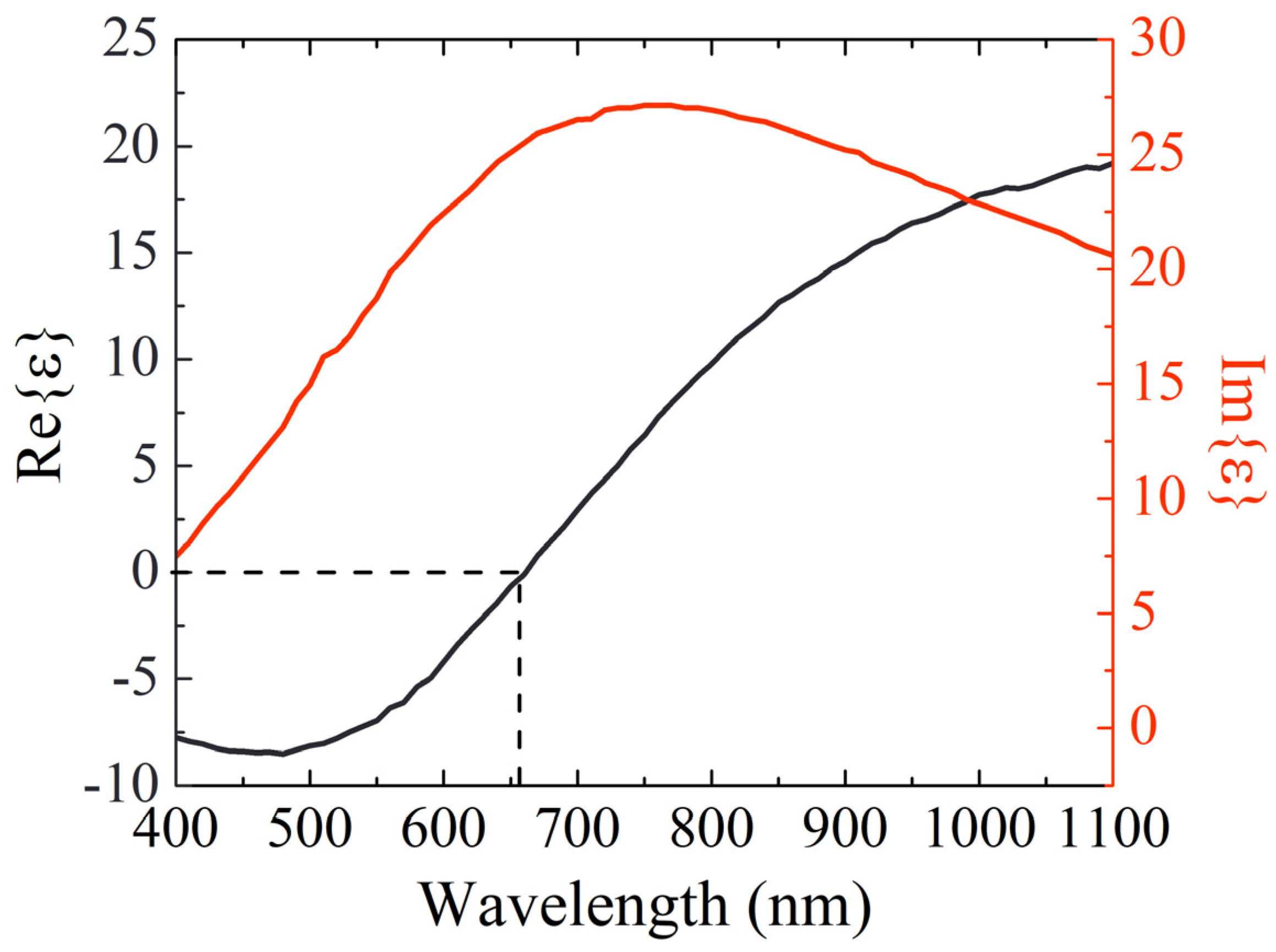
Figure 1 shows the real and imaginary parts of the dielectric constant of the BSTS film, which supports a zero real part at a wavelength of ~670 nm. Notably, the imaginary part is very considerable, which results in a high heat dissipation rate.
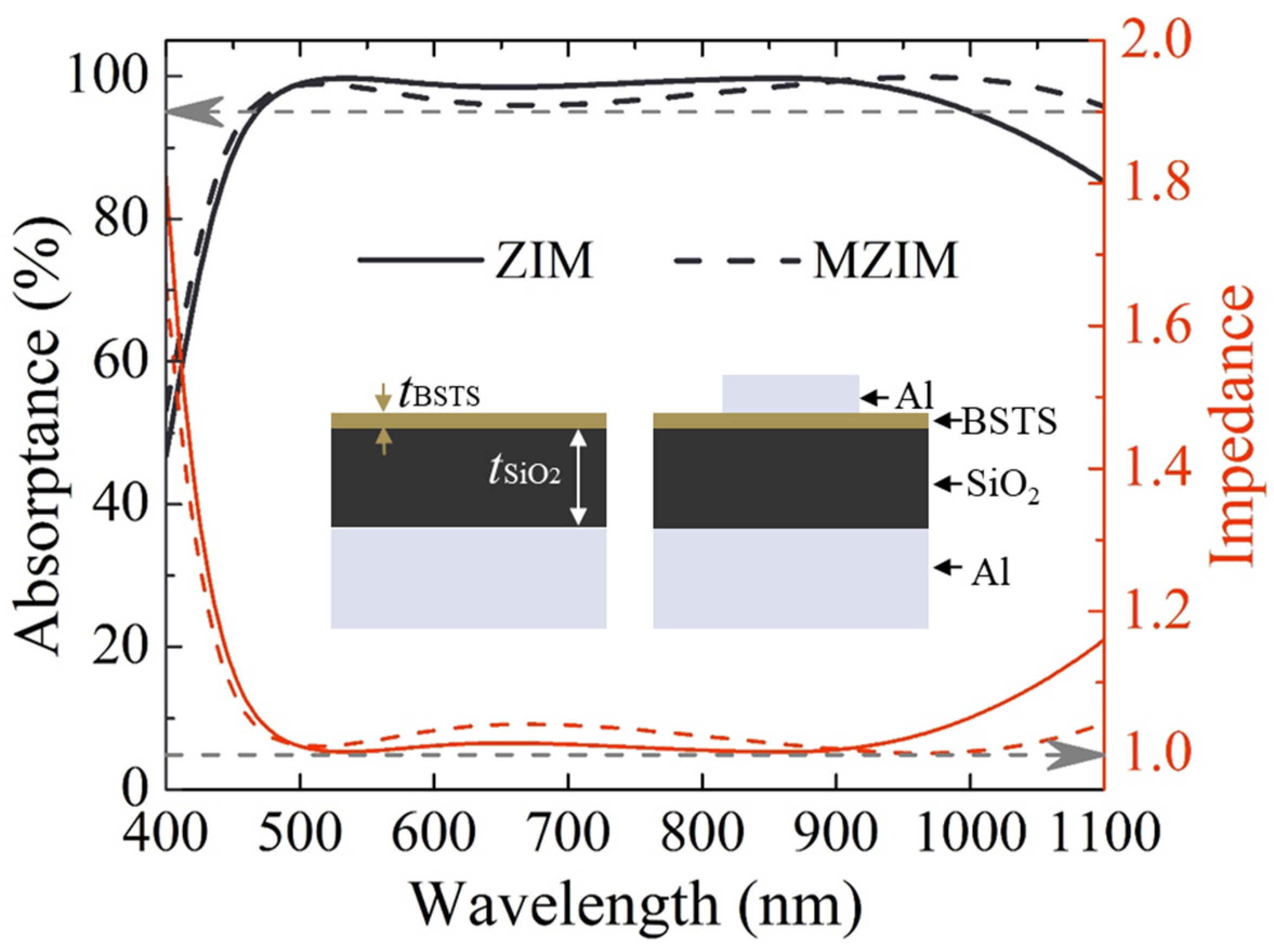
The proposed structure, consisting of three layers—i.e., ENZ, insulator, and metal (ZIM)—is schematically shown in the left inset of Figure 2. To characterize the absorption performance, the thicknesses of BSTS and SiO2 are optimized to be 5 and 100 nm, respectively. A plane wave is normally incident on the structure. Significantly, the absorption can be as high as 95%, covering the wavelength ranging from 470 to 1000 nm with a bandwidth of 72%, as the solid black line shows in Figure 2. Furthermore, a high absorptance of >99% can be maintained in a considerable wavelength band ranging from 500 to 918 nm with a bandwidth of 58% centered at the wavelength of 710 nm, which is close to the ENZ wavelength of 670 nm.
Meanwhile, the absorptance of a typical perfect absorber structure is also calculated for comparison. As the right inset shows in Figure 2, a metal Al block is added on the top of the ZIM structure with the other parameters unchanged, which is named as MZIM. As the black dashed line shows in Figure 2, the band with an absorptance of >95% covers the wavelength ranging from 460 to 1100 nm with a bandwidth of 82%. In comparison with the ZIM structure, the absorptance increases after 900 nm, and slightly decreases in the middle wavelength range. Although the high absorption band of the proposed ZIM structure is relatively narrower, the absence of the top Al block will significantly alleviate the complexity of the fabrication liability. As a result, the ZIM is more favorable to practical applications. To explore the working mechanism of the broadband absorption, the effective impedance (Z) of both the ZIM and MZIM structures is calculated by [28]:
Z   = ± ( 1 + S 11 ) 2 S 21 2 ( 1 S 11 ) 2 S 21 2 ,
where S11 and S21 represent the reflection and transmission coefficients of the system, respectively. Here, S11 can be extracted from the simulation and S21 = 0 due to the optically thick Al substrate. As shown in Figure 2, the high absorption band matches well with the wavelength range of the impedances of the vacuum for both the ZIM and MZIM structures. Therefore, the outstanding absorption performance can be attributed to the impedance matching between the environment and the entire structure. The lossy BSTS layer will then take charge of energy dissipation in the entire system. In the near infrared range, the decrease in the absorptance of the ZIM structure can be mainly contributed to the larger mismatch in impedance caused by the larger positive dielectric constant. However, for the MZIM structure, the resonance initiated by the top Al block still works well, and therefore the corresponding absorptance remains higher.
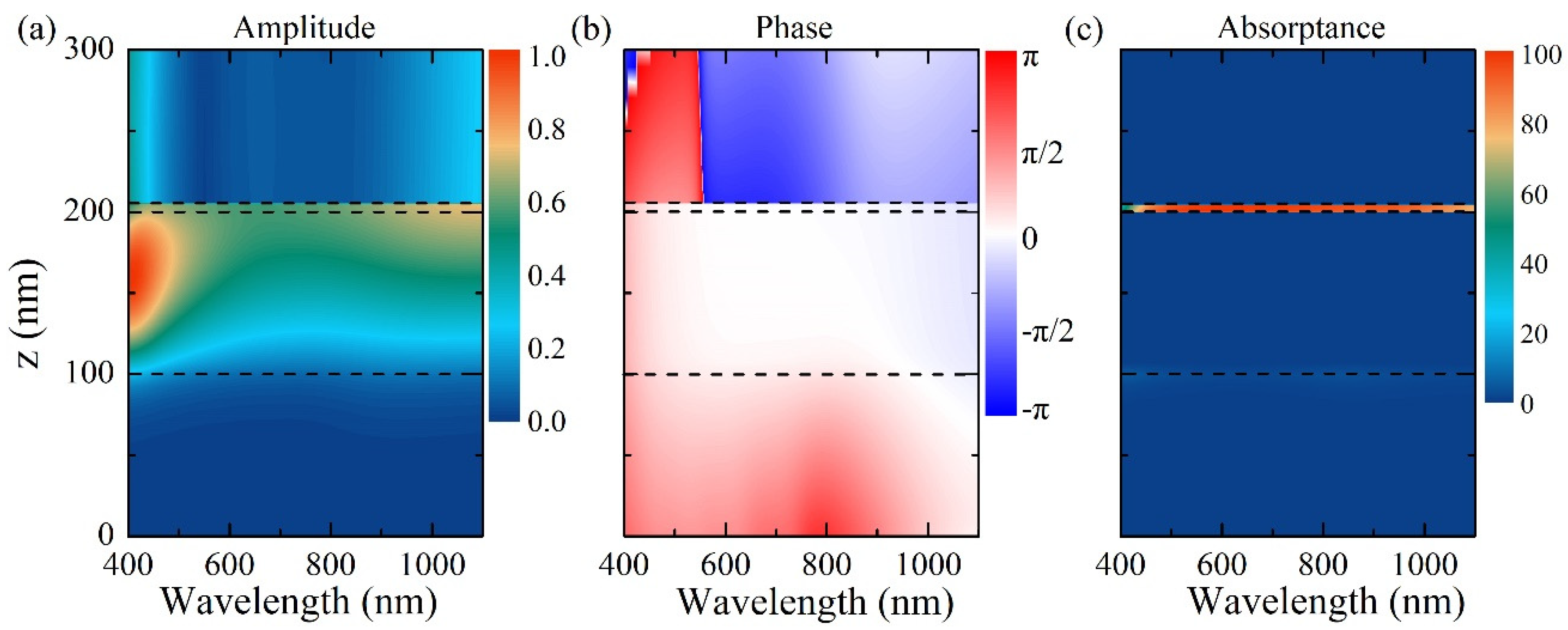
The ZIM structure resembles an asymmetric Fabry–Perot (FP) nanocavity composed of a lossless spacer layer with a top partially transparent/reflective lossy layer and backside reflector [29,30]. In comparison with the conventional FP-type cavity, which usually exhibits a highly wavelength selective feature in transmission or reflection spectra, the resonance character of the proposed ZIM structure shows a broadband response. The main reason can be attributed to the introduction of the high-loss top BSTS layer and Al substrate. The distributions of the electric field, field phase, and absorbed power over the cross section are plotted in Figure 3. The electric fields are highly confined by the boundary reflective BSTS and Al substrate. In particular, as depicted in Figure 3a, the fields are trapped in the dielectric layer not only at a resonance wavelength but across the absorption band, which indicates the same origin of the field trapping effect. The variation in the trapping schemes for different wavelengths arises from the different penetration depths into the cavity as well as material dispersions. However, the imaginary part of the permittivity of BSTS is much higher than the common noble metals, such as gold and aluminum, at the operation band. As known, a higher loss will result in a broader resonant bandwidth. As shown in Figure 3b, the uniformity of the phase change of the trapped wave inside the dielectric layer further confirms the broadband light trapping and absorption mechanism.
The BSTS layer plays a crucial role in the absorption process. As the calculated distribution of the absorbed power shows in Figure 3c, the top ENZ layer absorbs over 99% of the incident energy, which is consistent with its high-loss nature. Only tiny part of the incident energy is absorbed by the Al substrate in the planar-type multilayer perfect absorber. Subsequently, it will be found that the Al substrate will play a growing role in the energy absorption when curved surfaces are taken into consideration.
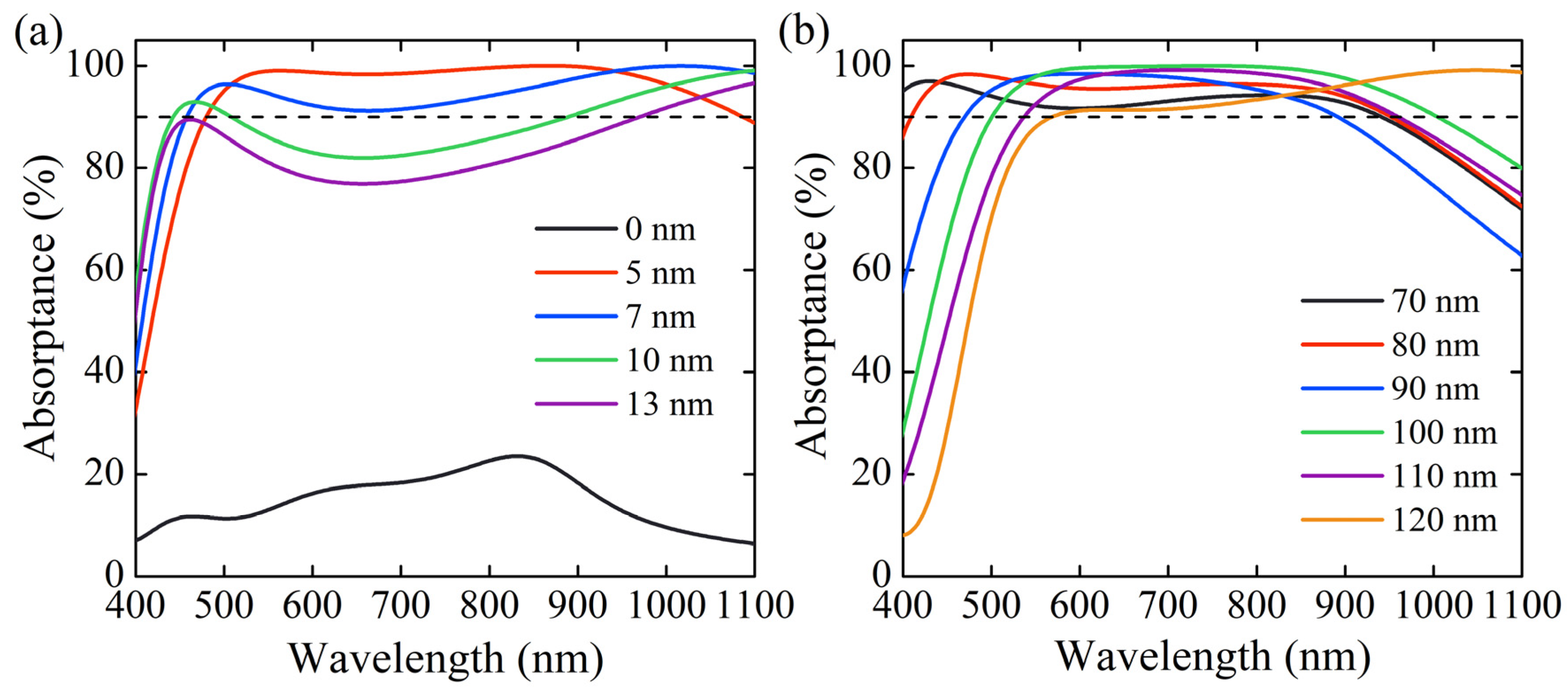
The proposed multilayer ZIM structure holds a great simplicity. Basically, an optimized absorption can be achieved by engineering the thicknesses of the BSTS layer and the SiO2 layer. As depicted in Figure 4a, when there is no BSTS layer, the low absorptance mainly results from the loss of the Al substrate, with a maximum of less than 25%. However, the absorptance is significantly increased when a layer of BSTS film is added. As the thickness of the BSTS film increases, the absorptance reaches an optimized performance when tBSTS = 5 nm—i.e., a high absorptance and considerable bandwidth. Meanwhile, the central wavelength of the absorption curve remains pinned at ~670 nm as the thickness of the BSTS film varies. As the thickness of the BSTS layer increases further, the absorptance of ~670 nm shows a more pronounced decline. Essentially, the thickness of the BSTS layer is critically responsible for the trade-off between light penetration and structure absorption. The reduction in absorption for the thicker BSTS film arises from the stronger blocking effect, which weakens the interaction strength between the incident energy and the structures.
In contrast, the thickness of the spacer layer SiO2 has a slight influence on the absorptance. As shown in Figure 4b, by varying the thickness of the SiO2 layer from 70 to 120 nm, the absorption band slightly shifts, but the absorptance maintains as high as 90% in a broadband, which indicates a fine robustness to the variation in the spacer. In particular, when the thickness of SiO2 is 100 nm, the bandwidth of absorptance >99% is optimized, with a center close to the ENZ wavelength.
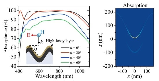
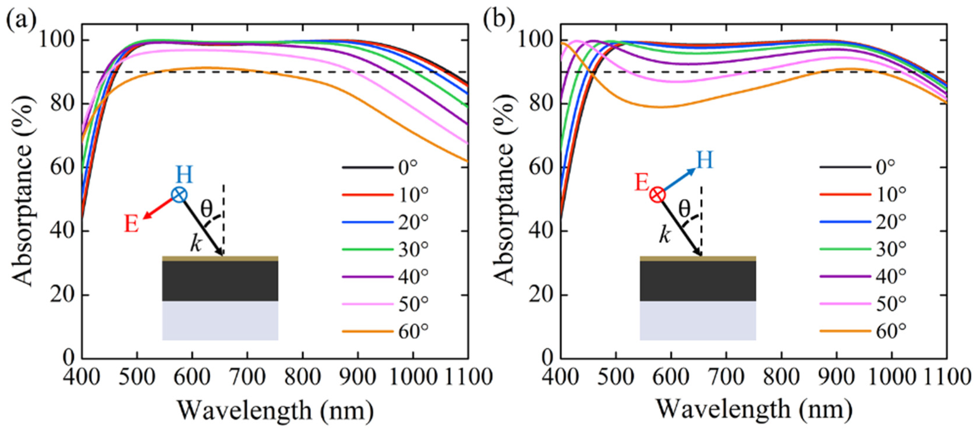
Due to the resonant effect, the optical response of the nanostructure is generally dependent on the angle of the incident light. Therefore, the performance of resonance-based perfect absorbers gets degraded as the incident angle increases, in particular for oblique angle incidences. To further investigate the performance, the absorption spectra of the optimized ZIM structure are also calculated as the incident angle increases from 0° to 60° under both transverse-magnetic (TM) and transverse-electric (TE) polarizations, as shown in Figure 5. For planar-type structures, the designed absorber is polarization-insensitive at a normal incidence, whereas for oblique incidence, the TM and TE polarizations exhibit different absorption behaviors. As shown in Figure 5a, a high and plateau absorption band remains as the incident angle approaches 50° under TM-polarized illumination. For larger incident angles, the obvious absorptance degradation occurs at a long wavelength side.
In contrast, under TE-polarized illumination, the flat absorption band remains even when the incident angle reaches 40°, as shown in Figure 5b. The absorption on the shorter wavelength side even increases for larger incident angles. On the other hand, the absorption at the long-wavelength edge decreases slightly with an amount smaller than the counterparts observed under TM polarization. In a sharp contrast, an obvious decrease occurs at the middle absorption band. Therefore, the flat-band absorption is not only independent of the light polarization for normal incidence, but also immunes from the incident angle even up to ±40°. The angle-dependent absorptance of the MZIM structure under both TM and TE-polarized lights are also calculated (not shown here). Similar to the ZIM structure, the absorptance of the MZIM structure is insensitive to the incident angle of TM-polarized light, whereas it is highly dependent on the incident angle of TE-polarized light due to the polarization-dependent resonance. In contrast, the electric field of TE-polarized incident light oscillates along the Al nanowire direction. Therefore, the MZIM structure has an obviously isotropic resonant response.
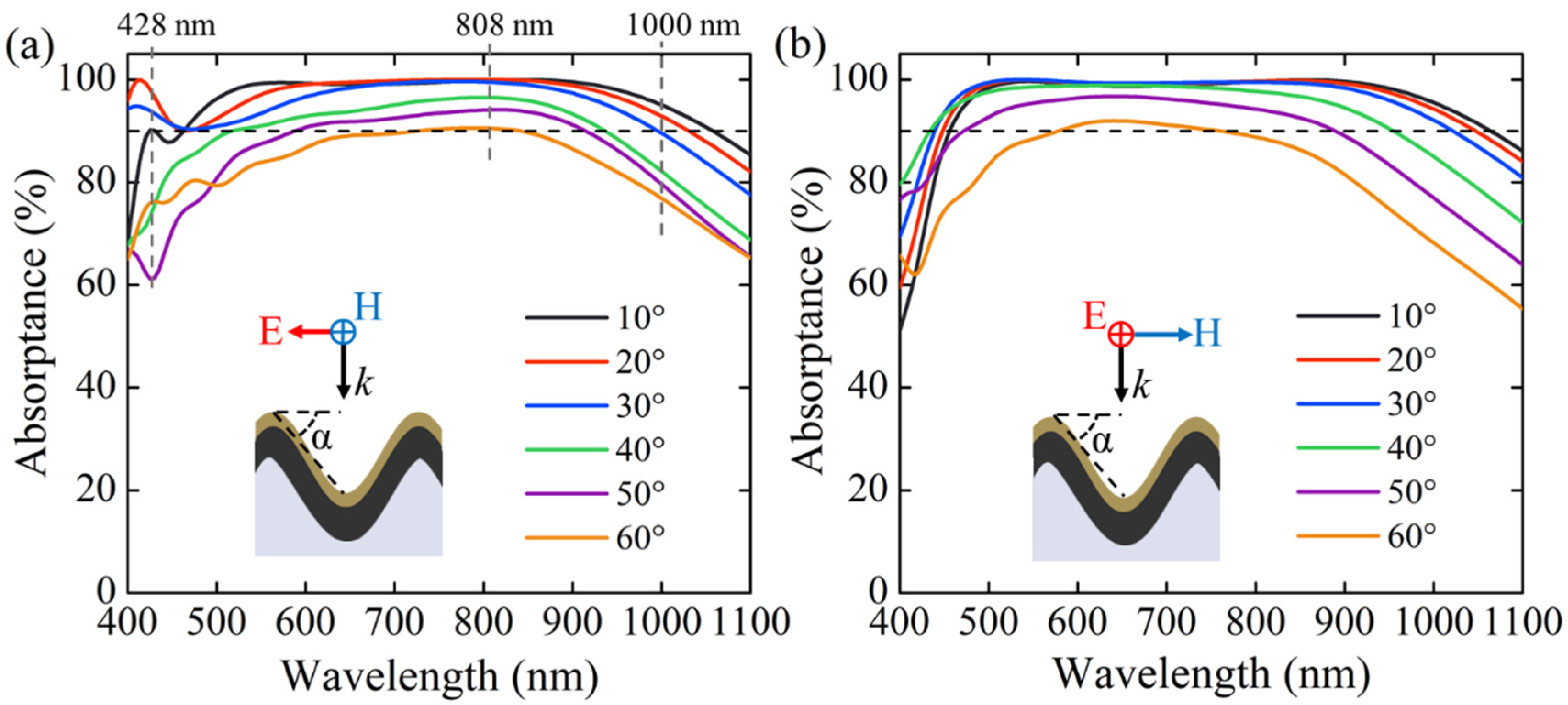
In practical scenarios, the surface of devices could be rough or even with curtained curved features, which require the perfect absorption to be robust to the curvature of the surface. As shown in Figure 5, the absorptance of the proposed ZIM structure can operate well under a broad angle incidence, therefore it can be potentially applied to complex surfaces. Therefore, the absorptance of structures with sinusoidal surface fluctuation are calculated under both TM and TE polarizations. Here, a geometry angle α is defined in the inset of Figure 6. A periodic condition is applied to calculate the absorptance and field distribution of the curved structures, where the Al substrate is optically thick (> the skin depth of Al in the operation wavelength) to block the transmission. As α increases from 10° to 60°, the real incident angle could be even larger than 70° relative to the surface normal at waist of the curvature. Furthermore, since the curvatures of each layer—i.e., the BSTS, SiO2, and Al substrate—are designed with the same sinusoidal function, the vertical thicknesses (along z-axis) of BSTS and SiO2 are 5 and 100 nm, respectively. As a result, the thickness of each layer along the normal direction to the surface changes with the coordinates, as schematically shown in the inset of Figure 6. Only the thicknesses at the top and bottom of the curvature are 5 and 100 nm for BSTS and SiO2, respectively, whereas the layer is thinner than the optimized parameters in planar ZIM. Remarkably, although the absorption decreases at the short and long wavelength sides of the spectrum, the absorption of the proposed curved ZIM structure changes slightly with the surface morphology variation at the center band ~670 nm for both TM and TE-polarized incidences. As shown in Figure 6, the absorptance remains higher than 90% even when α is 60°. More importantly, the excellent absorption performance is immune from the variations in the thickness of the BSTS and SiO2 layer. Therefore, the proposed ZIM structure could find wide applications as a conformal perfect absorber, with great simplification in comparison with structural metamaterials [31].
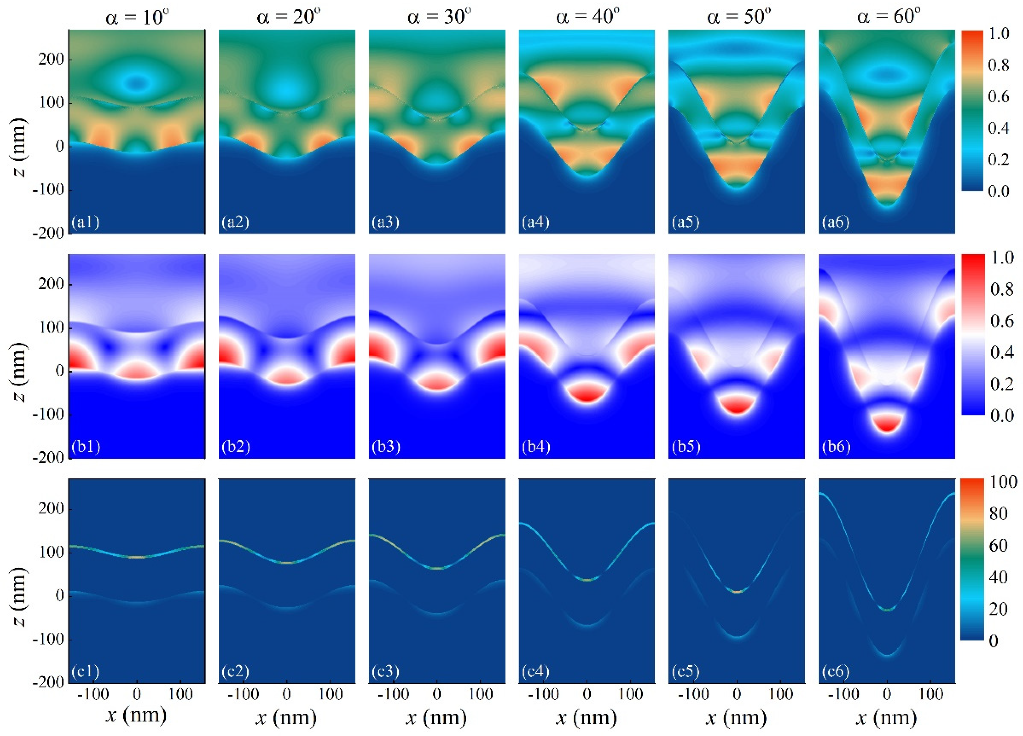
Although a high absorption band could be supported as the geometry angle increases, the absorption varies obviously at 428 nm under TM illumination, as labeled in Figure 6a. In order to analyze the underlying mechanism, the electric field, magnetic field, and absorption profiles at the wavelength of 428 nm are plotted in Figure 7 as the geometric angles increases. As shown in Figure 3a, the electric field at 428 nm is mainly confined at the dielectric SiO2 layer for a planar multilayer design, which can be regarded as the geometry angle being 0. The low absorptance (~49.6%) mainly arises from the negligible absorption in the SiO2 layer. In contrast, the absorptance of the curved surface increases remarkably, which is >60% even when α = 60°. Such a remarkable increase in absorption can be understood from the perspective of field distributions. For planar structure, the field is uniformly distributed in the along x-axis. However, the spatial distributions of electric and magnetic field varies as the geometry angle increases. As shown in Figure 7(a1–a6), as the geometry angle increases, the electric field gradually exhibits standing-wave-like distributions in the dielectric layer and inside the top valley separately. The deeper valley could support higher-order standing waves. Furthermore, the electric field tends to be sucked into the gap for lager geometry angles. A similar standing-wave-like distribution is also applied to magnetic field, albeit being mainly confined to the dielectric layer. A shallow valley enhances the field confinement and thus lengthens the interaction strength between the incident light and dissipation layer. As shown in Figure 7(c1), in addition to the BSTS layer, incident energy starts to be dissipated at the surface of the Al substrate. Consequently, the total absorptance increases to 90% when α = 10°. The absorptance is further boosted up to 97% as α increases to 30°. However, as α increases to 40°, part of the electric field is confined to the valley, which holds a dipole-like feature. Therefore, the energy gets easier to be radiative to the far field and the absorptance decreases. As a results, less energy is dissipated in the BSTS layer, as shown in Figure 7(c4). The absorptance degrades further as α increases to 50° due to the stronger radiative effect. Nevertheless, the absorptance increases again when α = 60°, which results from an inefficient radiation since the field goes deeper inside the valley.
In addition, in the planar ZIM structure, the incident energy is almost fully absorbed in the BSTS layer. In contrast, the energy can be dissipated in the Al substrate in curved ZIMs, as shown in Figure 7(c1–c6). By comparing the magnetic field distribution with the absorption pattern, it can be found that the spatial distribution of absorptance at the Al substrate is consistent with the counterpart of the magnetic field. Therefore, the magnetic field is responsible for the absorption in the Al substrate. On the other hand, the electric field takes the responsibility of energy dissipation in the BSTS layer in both planar and curved ZIM structures. The relevance between the electric/magnetic field and absorption can be perceived in the distribution of absorption in Figure 7.
The fluctuation of the absorptance can only observed at the short wavelength side due to the standing wave-like effect, as shown in Figure 7. Comparatively, the absorptance decreases monotonically as α increases at long wavelength side (>500 nm), as shown in 
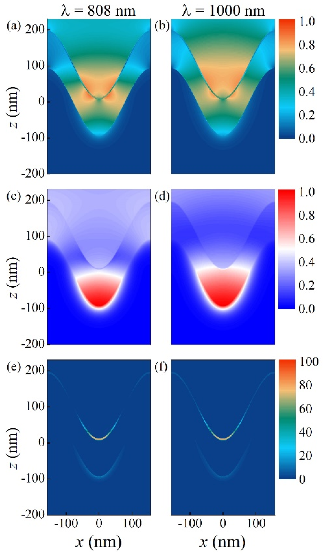
Figure 6. To investigate the dependence of absorption on the geometry angle, the distributions of electric field, magnetic field, and absorption are also plotted at the longer wavelengths of 808 and 1000 nm when α = 50°, as shown in Figure 8. As shown in Figure 8a,b, the electric fields are confined at the two interfaces of the BSTS layer and inside the valley, which mainly contribute to the absorption by the BSTS layer. In contrast, the magnetic fields are spread at the bottom of the SiO2 layer, which results in the energy dissipation at the SiO2/Al interface. In comparison with the field distribution at 428 nm, the standing wave-like effect can be negligible at the long wavelength side. In addition, the distribution of absorption area is almost continuous at the center part of valley, which further confirms the absence of the standing wave-like effect. Therefore, as the geometry angle increases, the absorptance decreases monotonically due to the strong scattering by the large slope of valleys. A similar trend also occurs for TE-polarized illumination.
Herein, the ENZ material is chosen to be BSTS, with an ENZ wavelength of 670 nm. Indeed, abundant ENZ materials can be found in homogenous materials, such as metals, doped semiconductors, and phononic materials, with ENZ wavelengths ranging from ultraviolet to infrared frequency. Moreover, structured materials such as metamaterials, waveguides near the cutoff frequency, resonant cavities, and photonic crystals provide a more versatile platform to engineer the operation wavelength of ENZ materials, or even ones with tunable properties [32]. Therefore, it is foreseen that the proposed ZIM structure can be readily extend to other bands for perfect absorber design.
In practice, the proposed ZIM structure is feasible. At first, a 100 nm-thick SiO2 can be readily deposited on Al substrate. It is also believed that a 5 nm-thick BSTS film could be possible. As shown in our previous work, a 5 nm-thick Bi2Te3, another type of topological insulator, can be fabricated in an experiment [33]. Therefore, the proposed perfect absorber in this work could be fabricated in the future.

3. Conclusions

To conclude, a trilayer perfect absorber—i.e., ZIM structure—is numerically demonstrated over the visible and near infrared bands by involving a layer of BSTS film. After judiciously optimizing the thickness of each layer, a polarization-independent perfect absorber over a broad band is realized even when the incident angle is as large as 50°, which suggests a conformal perfect absorber to be applicable to a device surface with a complex morphology. The absorptance remains as high as >99% over the wavelength ranging from 575 to 855 nm with a bandwidth of 39%, which outperforms the existing works. Furthermore, due to the multilayer configuration, the proposed scheme is very amicable to the current nanofabrication process. At last, by evaluating the absorption performance of the curved ZIM structure, the broadband high absorptance can be preserved even when the geometry angle approaches 50°, and is immune from slight variations in the thicknesses of the ENZ and SiO2 layers. The realized perfect conformal absorber using ZIM structures could act as a promising role for a wealth of absorption-related applications. Moreover, the involvement of ENZ can also open an exciting avenue to designing metamaterials for robust and enhanced optical functionalities.

Author Contributions

L.Z. proposed the idea and performed the initial simulations. K.W. performed the calculations and visualized the results. L.Z. and K.W. drafted the manuscript. K.W., H.C., Y.Z., and L.Z. discussed the results and revised the manuscript. L.Z. supervised the project. All the authors have read and agreed to the published version of the manuscript. All authors have read and agreed to the published version of the manuscript.

Funding

This research was funded by Natural Science Foundation of Shaanxi Province (2018JM6001); Fundamental Research Funds for the Central Universities of Xi’an Jiaotong University (Z201805196); the Young Talent Recruiting Plans of Xi’an Jiaotong University.

Conflicts of Interest

The authors declare no conflict of interest.

References

  1. Atwater, H.A.; Polman, A. Plasmonics for improved photovoltaic devices. Nat. Mater. 2010, 9, 205–213. [Google Scholar] [CrossRef] [PubMed]
  2. Wang, Z.; Tong, Z.; Ye, Q.; Xu, H.; Nie, X.; Yan, C.; Shang, W.; Song, C.; Wu, J.; Wang, J.; et al. Dynamic tuning of optical absorbers for accelerated solar-thermal energy storage. Nat. Commun. 2017, 8, 1478. [Google Scholar] [CrossRef] [PubMed]
  3. Chen, K.; Adato, R.; Altug, H. Dual-band perfect absorber for multispectral plasmon-enhanced infrared spectroscopy. ACS Nano 2012, 6, 7998–8006. [Google Scholar] [CrossRef]
  4. Lin, K.T.; Chen, H.L.; Lai, Y.S.; Yu, C.C. Silicon-based broadband antenna for high responsivity and polarization-insensitive photodetection at telecommunication wavelengths. Nat. Commun. 2014, 5, 3288. [Google Scholar] [CrossRef] [Green Version]
  5. Kuznetsov, S.A.; Paulish, A.G.; Navarro-Cía, M.; Arzhannikov, A.V. Selective pyroelectric detection of millimetre waves using ultra-thin metasurface absorbers. Sci. Rep. 2016, 6, 21079. [Google Scholar] [CrossRef] [PubMed] [Green Version]
  6. Liu, X.L.; Starr, T.; Starr, A.F.; Padilla, W.J. Infrared spatial and frequency selective metamaterial with near-unity absorbance. Phys. Rev. Lett. 2010, 104, 207403. [Google Scholar] [CrossRef] [Green Version]
  7. Hao, J.M.; Wang, J.; Liu, X.L.; Padilla, W.J.; Zhou, L.; Qiu, M. High performance optical absorber based on a plasmonic metamaterial. Appl. Phys. Lett. 2010, 96, 251104. [Google Scholar] [CrossRef]
  8. Cui, Y.X.; Fung, K.H.; Xu, J.; Ma, H.J.; Jin, Y.; He, S.L.; Fang, N.X. Ultrabroadband light absorption by a sawtooth anisotropic metamaterial slab. Nano Lett. 2012, 12, 1443–1447. [Google Scholar] [CrossRef] [Green Version]
  9. Guo, W.L.; Liu, Y.X.; Han, T.C. Ultra-broadband infrared metasurface absorber. Opt. Express 2016, 24, 20586. [Google Scholar] [CrossRef]
  10. Pang, Y.Q.; Li, Y.F.; Yan, M.B.; Liu, D.Q.; Wang, J.F.; Xu, Z.; Qu, S.B. Hybrid metasurfaces for microwave reflection and infrared emission reduction. Opt. Express 2018, 26, 11950. [Google Scholar] [CrossRef]
  11. Liu, N.; Mesch, M.; Weiss, T.; Hentschel, M.; Giessen, H. Infrared absorber and its applications as plasmonic sensor. Nano Lett. 2010, 10, 2342–2348. [Google Scholar] [CrossRef] [PubMed]
  12. Chang, Y.-C.; Kildishev, A.V.; Narimanov, E.E.; Norris, T.B. Metasurface perfect absorber based on guided resonance of a photonic hypercrystal. Phys. Rev. B 2016, 94, 155430. [Google Scholar] [CrossRef] [Green Version]
  13. Ra’di, Y.; Asadchy, C.S.; Kosulnikov, S.U.; Omelyanovich, M.M.; Morits, D.; Osipov, A.V.; Simovski, C.R.; Tretyakov, S.A. Full light absorption in single arrays of spherical nanoparticles. ACS Photonics 2015, 2, 653–660. [Google Scholar] [CrossRef]
  14. Monti, A.; Alù, A.; Toscano, A.; Bilotti, F. The design of optical circuit-analog absorbers through electrically small nanoparticles. Photonics 2019, 6, 26. [Google Scholar] [CrossRef] [Green Version]
  15. Moreau, A.; Ciracì, C.; Mock, J.J.; Hill, R.T.; Wang, Q.; Wiley, B.J.; Chilkoti, A.; Smith, D.R. Controlled-reflectance surfaces with film-coupled colloidal nanoantennas. Nature 2012, 492, 86–89. [Google Scholar] [CrossRef] [Green Version]
  16. Li, Z.Y.; Butun, S.; Aydin, K. Ultranarrow band absorbers based on surface lattice resonances in nanostructured metal surfaces. ACS Nano 2014, 8, 8242–8248. [Google Scholar] [CrossRef] [PubMed]
  17. Monti, A.; Alù, A.; Toscano, A.; Bilotti, F. Narrowband transparent absorbers based on ellipsoidal nanoparticles. Appl. Opt. 2017, 56, 7533–7538. [Google Scholar] [CrossRef]
  18. Xia, S.; Zhai, X.; Huang, Y.; Liu, J.; Wang, L.; Wen, S. Multi-band perfect plasmonic absorptions using rectangular graphene gratings. Opt. Lett. 2017, 42, 3052. [Google Scholar] [CrossRef]
  19. Yu, W.W.; Lu, Y.; Chen, X.R.; Xu, H.; Shao, J.; Chen, X.; Sun, Y.; Hao, J.M.; Dai, N. Large-area, broadband, wide-angle plasmonic metasurface absorber for midwavelength infrared atmospheric transparency window. Adv. Opt. Mater. 2019, 7, 1900841. [Google Scholar] [CrossRef] [Green Version]
  20. Mou, N.L.; Liu, X.L.; Wei, T.; Dong, H.X.; He, Q.; Zhou, L.; Zhang, Y.Q.; Zhang, L.; Sun, S.L. Large-scale, low-cost, broadband and tunable perfect optical absorber based on phase-change material. Nanoscale 2020, 12, 5374. [Google Scholar] [CrossRef]
  21. Kats, M.A.; Blanchard, R.; Genevet, P.; Capasso, F. Nanometre optical coatings based on strong interference effects in highly absorbing media. Nat. Mater. 2013, 12, 20–24. [Google Scholar] [CrossRef] [PubMed]
  22. You, J.; Lee, W.; Won, D.; Yu, K. Multiband perfect absorbers using metal-dielectric films with optically dense medium for angle and polarization insensitive operation. Opt. Express 2014, 22, 8339. [Google Scholar] [CrossRef] [Green Version]
  23. Rensberg, J.; Zhou, Y.; Richter, S.; Wan, C.H.; Zhang, S.Y.; Schöppe, P.; Schmidt-Grund, R.; Ramanathan, S.; Capasso, F.; Kats, M.A.; et al. Epsilon-near-zero substrate engineering for ultrathin-film perfect absorbers. Phys. Rev. Appl. 2017, 8, 014009. [Google Scholar] [CrossRef]
  24. Kinsey, N.; Khurgin, J. Nonlinear epsilon-near-zero materials explained: Opinion. Opt. Mater. Express 2019, 9, 2793. [Google Scholar] [CrossRef]
  25. Li, Z.Y.; Palacios, E.; Butun, S.; Kocer, H.; Aydin, K. Omnidirectional, broadband light absorption using large-area, ultrathin lossy metallic film coatings. Sci. Rep. 2015, 5, 15137. [Google Scholar] [CrossRef]
  26. Ghobadi, A.; Dereshgi, S.A.; Hajian, H.; Bozok, B.; Butun, B.; Ozbay, E. Ultra-broadband, wide angle absorber utilizing metal insulator multilayers stack with a multi-thickness metal surface texture. Sci. Rep. 2017, 7, 4755. [Google Scholar] [CrossRef]
  27. Ou, J.; So, J.; Adamo, G.; Sulaev, A.; Wang, L.; Zheludev, N.I. Ultraviolet and visible range plasmonics in the topological insulator Bi1.5Sb0.5Te1.8Se1.2. Nat. Commun. 2014, 5, 5139. [Google Scholar] [CrossRef] [Green Version]
  28. Chen, X.D.; Grzegorczyk, T.M.; Wu, B.I.; Pacheco, J., Jr.; Kong, J.A. Robust method to retrieve the constitutive effective parameters of metamaterials. Phys. Rev. E 2004, 70, 016608. [Google Scholar] [CrossRef] [Green Version]
  29. Shu, S.W.; Li, Z.; Li, Y.Y. Triple-layer Fabry-Perot absorber with near-perfect absorption in visible and near-infrared regime. Opt. Express 2013, 21, 25307. [Google Scholar] [CrossRef]
  30. Song, H.M.; Guo, L.Q.; Liu, Z.J.; Liu, K.; Zeng, X.; Ji, D.X.; Zhang, N.; Hu, H.F.; Jiang, S.H.; Gan, Q.Q. Nanocavity enhancement for ultra-thin film optical absorber. Adv. Mater. 2014, 26, 2737–2743. [Google Scholar] [CrossRef]
  31. Jiang, Z.H.; Yun, S.; Toor, F.; Werner, D.H.; Mayer, T.S. Conformal dual-band near-perfectly absorbing mid-infrared metamaterials coating. ACS Nano 2011, 5, 4641–4647. [Google Scholar] [CrossRef] [PubMed]
  32. Kinsey, N.; DeVault, C.; Boltasseva, A.; Shalaev, V.M. Near-zero-index materials for photonics. Nat. Rev. Mater. 2019, 4, 742–760. [Google Scholar] [CrossRef]
  33. Yuan, J.; Ma, W.; Zhang, L.; Lu, Y.; Zhao, M.; Guo, H.; Zhao, J.; Yu, W.; Zhang, Y.; Zhang, Y.; et al. Infrared Nanoimaging reveals the surface metallic plasmons in topological insulator. ACS Photonics 2017, 4, 3055–3062. [Google Scholar] [CrossRef]
Figure 1. Real (black line) and imaginary (red line) parts of the permittivity of the Bi1.5Sb0.5Te1.8Se1.2 (BSTS) film. The real part of the permittivity is close to zero at a wavelength of 670 nm.
Photonics 07 00057 g001
Figure 2. Comparison of the absorptance and impedance for different structures. The thicknesses of the BSTS film are SiO2 tBSTS = 5 nm and tSiO2 = 100 nm, and the Al substrate is optically thick to block the light transmission. In the MZIM structure, 30 nm-high and 20 nm-wide Al wire arrays are positioned on the top, with a periodicity of 100 nm. The upper grey dashed line indicates an absorptance of 95%, while the lower one specifies an impedance of 1.
Photonics 07 00057 g002
Figure 3. Distributions of the (a) electric field amplitude, (b) phase, and (c) absorptance as a function of the wavelength for the ZIM structure. The dashed lines are plotted to indicate the interface between different materials. Here, tBSTS = 5 nm and tSiO2 = 100 nm.
Photonics 07 00057 g003
Figure 4. Dependence of the absorptance of the ZIM structure on the thickness of (a) the BSTS layer by fixing tSiO2 = 100 nm and (b) the SiO2 layer by fixing tBSTS = 5 nm. Linear polarized light is normally incident on the ZIM structure. Dashed lines represent an absorptance of 90%.
Photonics 07 00057 g004
Figure 5. Dependence of the absorptance of the ZIM structure on the incident angle under the illumination of (a) TM and (b) TE-polarized incident lights. Here, tBSTS = 5 nm and tSiO2 = 100 nm. Insets show the simulation configurations.
Photonics 07 00057 g005
Figure 6. Dependence of the absorptance of a conformal structure on the geometric angle α under the illumination of (a) TM and (b) TE-polarized incident lights. Here, tBSTS = 5 nm and tSiO2 = 100 nm. Note: the thickness is measured along the z-axis in the following simulations. The surface curvature is defined as z = Asin (2πx/p), where the periodicity p is 314 nm and A is the amplitude. The geometry angle can thus be defined as α= atan (4A/p).
Photonics 07 00057 g006
Figure 7. Calculated distributions of the normalized electric field (a1a6), normalized magnetic field (b1b6), and absorption (c1c6) at 428 nm as the geometry angle α increases from 10° to 60° under the illumination of TM-polarized light propagating along the z-axis. Here, tBSTS = 5 nm and tSiO2 = 100 nm.
Photonics 07 00057 g007
Figure 8. Calculated distributions of the normalized electric field (a,b), normalized magnetic field (c,d), and absorption (e,f) at wavelengths of 808 and 1000 nm when the geometry angle α is 50° under the illumination of TM-polarized light propagating along the z-axis. Here, tBSTS = 5 nm and tSiO2 = 100 nm.
Photonics 07 00057 g008

