Article

Insights of Hysteresis Behaviors in Perovskite Solar Cells from a Mixed Drift-Diffusion Model Coupled with Recombination

Harbin Institute of Technology, School of Mechatronics Engineering, Harbin 150001, China
*
Author to whom correspondence should be addressed.
Photonics 2020, 7(3), 47; https://doi.org/10.3390/photonics7030047
Submission received: 6 June 2020 / Revised: 25 June 2020 / Accepted: 2 July 2020 / Published: 3 July 2020
(This article belongs to the Special Issue Wide Bandgap Semiconductor Photonic Devices)

Abstract

:
Hysteresis in perovskite solar cells is a notorious issue limiting its development in stability, reproducibility and efficiency. Ions’ migration coupled with charges’ recombination are indispensable factors to generate the hysteretic curves on the basis of experimental and theoretical calculation studies, however, the underlying physical characteristics are rarely clarified. Here, a mixed electronic-ionic drift-diffusion model combined with bulk and interfacial recombination is investigated. Positive and negative ion species could drift to and accumulate at interfaces between the perovskite/transport layers, influencing internal electric potential profiles and delaying the charges’ ejection to the transport layers. The charges might recombine spontaneously or trap-assisted, reducing the total amount of electrons and holes collected in the external circuit, leading to a diminished photocurrent. Moreover, our calculations indicate that an appropriate measurement protocol is really essential to evaluate the device performance precisely and to suppress J–V hysteresis. Meanwhile, a negligible hysteretic loop could be obtained by balancing the material properties of the transport layers and restraining the ions mobility in the perovskite layer.

Graphical Abstract

1. Introduction

Research enthusiasm on organic–inorganic perovskite solar cells (PSCs) has risen tremendously within the last decade, attributed to their remarkable optoelectronic properties, such as high carrier mobility, suitable band gap and excellent economic efficiency [1]. Seok et al. [2] published a certified power conversion efficiency (PCE) of 23.73% by stabilizing α-phase formamidinium lead iodide (FAPbI3) with methylenediammonium dichloride (MDACl2) dopant material, and their lab-measured champion device presented a PCE of 24.66%; meanwhile, the NREL (National Renewable Energy Laboratory, U.S.) best research-cell efficiencies presented a record of 25.2% [3]. Moreover, the perovskite/silicon tandem solar cells have achieved a PCE of 26.7% recently [4]. Despite the fact that numerous achievements have been obtained to commercialize the PSCs, one of the major barriers is photocurrent hysteresis, over or underestimating the device performance [5]. The hybrid perovskite materials were reported to be combined conductors of electrons and ions [6]. Experimental and theoretical studies indicated that the iodine (I) and the methylammonium (MA+) are the major available mobile ion species in the perovskite material of methylammonium lead triiodide (MAPbI3) [7]. Furthermore, it is these ions’ migration combined with trap-assisted recombination that give rise to the anomalous current density–voltage (J–V) hysteresis [8,9]. However, it has yet to be clearly clarified what characteristics inside the PSC are modified if the ions could migrate regularly and what functions of the recombination act as to induce the hysteretic phenomena. Besides, numerical research work on the improvement of measurement protocols and material properties to suppress J–V hysteresis is rarely performed.
A range of approaches have been studied to model the characteristics of the PSCs. Density functional theory (DFT), based on the first principle, is widely used to calculate the microscopic properties of the perovskite materials [10]. Eames et al. [11] estimated the activation energies for different ion species using DFT calculation, and the results present 0.58, 0.84 and 2.31 eV for I, MA+ and Pb2+, respectively. A significant limitation for DFT study is the massive computational cost, and it is infeasible to calculate the entire PSC device structure with complicated boundary conditions. In this case, the drift-diffusion model is capable of explaining the macroscopic performance based on the microscopic properties, utilizing the conservation of charge carriers coupled with the balance of electric potential. Van Reenen et al. [9] firstly combined the mobile ions into the PSC drift-diffusion simulations to reproduce the experimental hysteretic phenomena, assuming an unrealistically high ion mobility and a high scan speed. Richardson et al. [12] implemented an asymptotic analysis of a single perovskite layer including the mobile iodide ion vacancies. Calado et al. [13] investigated the entire PSC layers using the drift-diffusion method by simplifying the heterojunctions to homojunctions, neglecting the property differences between the perovskite layer and the electron and hole transport layers (ETL and HTL). Courtier et al. [14,15,16] systematically studied the algorithms to solve the drift-diffusion equations credibly and fast, while only the positive ions’ migration was concluded in their numerical model. All of the abovementioned calculations require very profound mathematical and programming knowledge, hostile to the non-expert. Shen [17] and Xiang [18] attempted to use a multi-physics platform to define the drift-diffusion process of the charge carriers and ion species in the PSC and reproduced the notorious hysteresis J–V curves as occurred in experiments. More deep mechanism study on the working principles of the mobile ions in J–V hysteresis is needed.
Hysteresis elimination is the ultimate goal to which the researchers are dedicated. Numerical and theoretical studies could give a general experimental guideline to modify material properties or manufacturing processes to passivate J–V hysteresis. However, research in this area is scarce. Recently, Courtier et al. [16] and Xiang et al. [18] investigated the influences of how the bulk recombination and the interfacial recombination affect the shape of the J–V hysteresis curves, and put forward a simple diagnosis criterion to determine which kind of recombination was dominantly occurring inside the PSCs, but failed to make a further study on how to eliminate J–V hysteresis. George Alexandru et al. [19] studied how the measurement protocols affected the normal and inverted J–V hysteresis curves, proposing to reduce the hysteresis by changing the pre-poling conditions. However, the pre-poling treatment could just deal with the superficial issue; the defects and hysteresis still exist inside the PSC.
In this work, a well-rounded drift-diffusion model combined with the constraints of Shockley Read Hall (SRH) recombination is performed to reveal the underlying factors that support the hysteresis phenomena in the PSCs. We show that both the mobile ions and the SRH recombination are necessary to generate the hysteretic J–V loops. The corresponding variations of electric field and potential during the J–V measurement are proposed to expose the nature of hysteresis. From the point of measurement protocol, a fast J–V scan rate is essential to suppress J–V hysteresis with great photovoltaic efficiency. A positive voltage pre-treatment facilitates the PSC to generate a superior efficiency performance with reduced hysteresis, while scan direction could significantly affect the extent and shape of the J–V hysteresis curves. From the point of material properties, in order to passivate J–V hysteresis effectively, doping concentration and relative permittivity of the ETL and the HTL are supposed to increase equivalently, while no significant effect to enhance them imbalanced. Furthermore, the ion movement inside the perovskite layer should be limited to further diminish J–V hysteresis.

2. Methods

A device configuration of metal contact/ETL (100 nm)/perovskite (400 nm)/HTL (100 nm)/metal contact was adopted to perform the calculations concerning the J–V hysteretic phenomena. The charge transport was assumed to be directly across the interfaces in one spatial dimension (x). In addition, the influences of morphology, composition and grain structure of the perovskite layer were neglected. Although these factors could not be calculated in our calculation directly, they determine the characteristics of the perovskite layer, such as permittivity, ion concentration and mobility, which are analyzed in Section 3.3. As seen in Figure 1, the calculation model defined the motion of the free electrons (n), holes (p), defect negative ions (N) and positive ions (P) using the time-dependent drift-diffusion equations [14,18], including the bulk recombination (Rbulk) occurring inside the perovskite layer and the interfacial recombination (RETL and RHTL) occurring at the ETL/perovskite and the perovskite/HTL interfacial junctions, respectively. Furthermore, all of the recombination mechanisms were ruled by the Shockley Read Hall (SRH) recombination [20]. The related mathematical equations and calculation methods were shown in the Supplementary Materials. At the ETL/perovskite interface, the conduction band (EC) matching facilitated the electrons to flow into the ETL, while the valence band (EV) offset prevented the holes from the perovskite layer. However, the electrons from the ETL and the holes from the perovskite might leak out via the defective ionic trap-assisted recombination, named the interfacial recombination; the same goes for the perovskite/HTL interface. Inside of the perovskite material, the electrons and holes could make a non-radiative recombination within a limited transport length and lifetime, named the bulk recombination. Additionally, photovoltaic generation (G) and radiative recombination (R) are added to the perovskite layer.
In order to highlight the J–V hysteresis loops, an electron/hole pseudo-lifetime of 10 ns for Rbulk and 0.2 ns for RETL and RHTL were chosen, referring to the published work [18]. Moreover, an additional radiative recombination was added in the perovskite layer to yield a VOC of about 1.3 V [21,22]. A uniform electron/hole generation rate of 3.3 × 1027 m−3 s−1 was enabled in the perovskite layer to produce a JSC of about 21 mA cm−2 [9,23]. The material parameters used in the model are listed in Table 1, based on the literature values; since the parameter values varied from the references, a median or average value was chosen here. The perovskite material was widely regarded as an intrinsic semiconductor [24]; compared to the ETL and the HTL, the concentration of charge carriers was very low at about 109~1011 m−3, and was assumed to be not doped [20]. The doping concentrations in the ETL and the HTL were set equally of 1024 m−3 to obtain a built-in electric potential (Ebi) of about 1 V [25], and their effects on the hysteresis are specified in Section 3.3. The influences of permittivities of the ETL, perovskite and HTL on J–V hysteresis were also investigated in the following discussion. The ionic movement and redistribution were only constrained inside the perovskite layer. The ion concentration and mobility in the perovskite layer were studied in Section 3.3 to suppress J–V hysteresis. Speaking of which, the variation of the parameter values in the following calculations might be unrealistic currently for material technology and are just put forward as a guideline for material development. The mobility of electrons and holes were set constant in this work, with the assumption that the scattering defects in the perovskite solar cell were fixed. The boundary conditions at the interfaces were ruled by the heterojunction model with continuous quasi-Fermi levels. The whole cell was defined to connect to an external circuit with an ideal ohmic contact to perform the voltage sweep. For the initial conditions and measurement protocol, the device was generally pre-biased with a positive voltage 1.2 V to reach an equilibrium condition. Then, the external applied voltage swept from 1.2 to −0.2 V (Reverse, R), and turned back to 1.2 V (Forward, F) immediately to fulfill a complete J–V loop. The voltage varied with a step of 20 mV, and the scan rate was 240 mV/s, unless otherwise stated for the specific studies.

3. Results and Discussion

3.1. Hysteresis Origin and Generating Principles

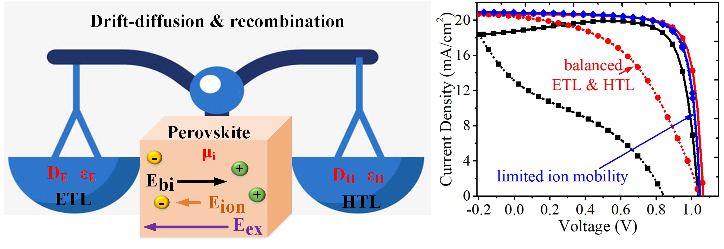
3.1.1. Essential Conditions for Hysteresis Reproduction Numerically

Firstly, in order to investigate J–V hysteresis in perovskite solar cells, we must reproduce the J–V hysteretic loops as reported experimentally. According to a previous study [26], the mobile ions and the recombination are the two generally accepted factors for the hysteresis phenomena, which were also discussed in our study theoretically, as seen in Figure 2. Consistent with the literature [27], we found that if the recombination (Rec) was not included in the calculation boundary conditions, the J–V curves present hysteresis-free, no matter if the ions were removable or stationary. This result indicates that recombination plays a dominant role in the J–V hysteresis phenomenon. On the other hand, if the calculations cover recombination, open circuit voltage (VOC) and short circuit current density (JSC) decreased; only by combining the ion species movement, the distinctive hysteresis curve could be obtained. The current decrease speed and the recombination rate present a large variation between the reverse (R) and the forward (F) scan. However, if no mobile ions are included, a hysteresis-free J–V curve was received. This calculation result is consistent with the published work [13,16], indicating the correctness of our calculation model. Only coupling the mobile ions and the recombination could obtain the hysteretic J–V curves, while no such effect was found when functionalizing them independently, and the recombination reduced the Voc and JSC.
Then, the influences of various combos of different recombination categories were investigated; the mobile ions were always calculated, as seen in Figure 2b,c. Compared to the cases with all of the three recombinations, we found that if the Rbulk was activated alone, the JSC decreased a little bit, while the forward VOC increased. In addition, if only RETL and RHTL were activated, the forward VOC decreased severely, while the JSC increased. This finding indicates that the Rbulk played a reverse role in comparison with the RETL and RHTL. We also investigated the RETL and RHTL independently, as seen in Figure 2c. The results show that the RETL almost had no effect on forward VOC, while reducing the forward JSC severely; the RHTL was the opposite to this effect. This unprecedented calculation result favored the assumption [28] that the imbalanced material properties in the ETL and the HTL could lead to an asymmetric transportation of electrons and holes, giving rise to the J–V hysteresis curves.

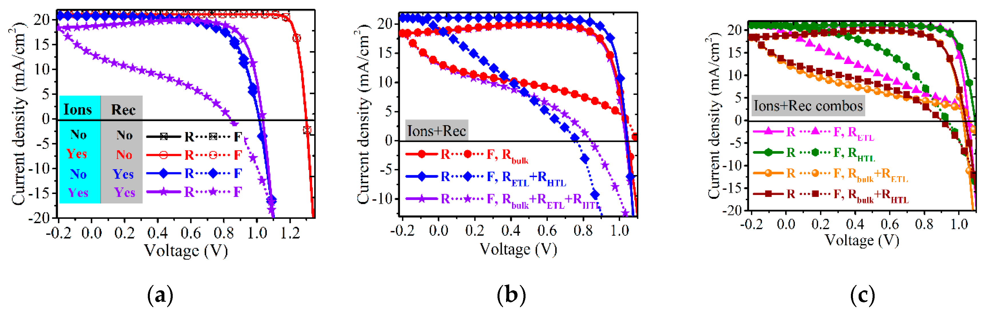
3.1.2. Hysteresis Generating Principles

The transformation of the charge carriers, ions and the resulting electric field are illustrated in Figure 3. With the pre-bias poling treatment by a positive external potential (Eex) of 1.2 V (>Ebi = 1 V), the positive ions drifted and accumulated to the ETL/perovskite interface, while the negative ions toward the HTL/perovskite interface, which could generate an ion-induced electric potential (Eion) across the perovskite layer with the rightward direction.
At the beginning of the reverse scan from 1.2 to 1 V (R-1 V), the energy band structure, charge movement and the possible recombination are presented in Figure 3a. Our calculation displayed an upward energy band with no resistance to the electrons and the holes’ transport to the ETL and the HTL, while preventing them flowing to the opposite layers. However, it might occur that these opposite-migrated charges recombine inside the perovskite layer—that is, the bulk recombination Rbulk; or recombine with the intrinsic charges located inside the adjacent transport layers—that is, the interfacial recombination RETL and the RHTL. In addition, due to the ions equilibration at the relaxation stage, the concentration of positive ions (P) was greater than that of negative ions (N) in the ETL/perovskite interface, as seen in Figure 4b, so the direction of Eion still kept rightward. In this case, Eex < Ebi + Eion, the direction of Etotal was same with the Eion, in agreement with the potential profiles in Figure 4a. The Etotal facilitated the free charges’ ejection to the external transport layers, and meanwhile, the ions began to drift around, following the Etotal.
When the reverse scan arrived at 0.5 V (R-0.5 V) and 0 V (R-0 V), as seen in Figure 4b, our calculation showed that the amount of N at the ETL/perovskite interface had been larger than that of the P, thus, the direction of Eion inverted compared to that at R-1 V, as shown in Figure 3b. Meanwhile, the potential remained downward, as presented in Figure 4a, indicating the rightward of the Etotal due to that Ebi > Eex + Eion. In addition, the potential drop in the perovskite layer at the interfaces also enlarged, combined with the more upward energy band structure, promoting the free charges’ ejection more efficiently [16]. Furthermore, attributing to the extended band offset at the interfaces, the interfacial recombination could be scarce, leaving a small amount of bulk recombination and a large current density compared to R-1 V. In addition, the gradient of potential profiles at R-0.5 V was larger than that at R-0 V, as seen in Figure 4a, which could favor charge carriers’ transportation more efficiently and reduce the recombination lost, resulting in increased current density at R-0.5 V compared to R-0 V in Figure 2.
When it came to the forward scan at 0, 0.5 and 1 V (F-0, F-0.5 and F-1 V), the calculation result shows that the concentration of N over-weighted that of P at the ETL/perovskite interface through the whole forward scan process, thus, the direction of Eion kept leftward. Combined with the upward potential profiles shown in Figure 4a, Eex + Eion > Ebi, the direction of Etotal was leftward and fully inverted compared to the reverse scan, as presented in Figure 3c. Combined with the downward energy band structure, most of the free charges were drifted and flowed to the wrong transport layers (that is, electrons to the HTL, and holes to the ETL), deteriorating the bulk and the interfacial recombination, inducing the small photocurrent at forward scan, as seen in Figure 2.
Above all, our calculation indicated that the recombination is supposed to play a more essential role than the ionic migration in the hysteresis phenomena. Specifically, it is the ionic movement that changes the electric field inside the perovskite layer, delaying the lossless ejection of the free charges, if excluding the recombination. However, it is the recombination that really reduces the number of electrons and holes to transport from the perovskite layer, causing the decreased photocurrent.

3.2. Measurement Protocols Improvement to Suppress Hysteresis
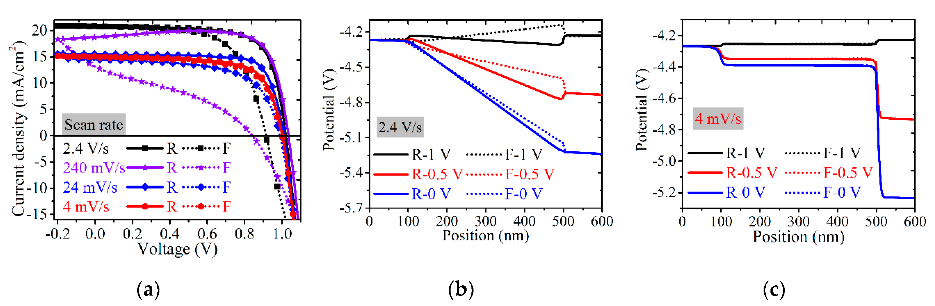
3.2.1. Scan Rates

Voltage scan rate has been reported and widely accepted to modify the hysteresis from the testing point [8,29]. The scan rate was varied through a triangle function, as seen in the Supplementary Materials Figure S1. As seen in Figure 5, the influences of the scan rates of 2.4 V/s, 240 mV/s, 24 mV/s and 4 mV/s were investigated by characterizing the J–V curves and the electric potential profiles across the device. We found that the very fast (>2.4 V/s) and the very slow (≤4 mV/s) scan rate could obtain J–V loops with negligible hysteresis, while the intermediate scan rate enlarged the gap between the forward and the reverse scan curves. In addition, it is worth mentioning that compared to the relatively high scan speed of 2.4 V/s and 240 mV/s, when the J–V measurement was conducted under slow scan rates of 24 mV/s and 4 mV/s, the JSC decreased severely, while the difference of JSC and VOC between the forward scan and reverse scan reduced.
The potential distribution at the scan rate of 2.4 V/s is presented in Figure 5b; compared to Figure 4a at a scan rate of 240 mV/s, we found that the potential profiles kept downward similarly in the stage of reverse scan, but the gradient was larger here, indicating that the strength of Etotal inside the perovskite solar cell became stronger, promoting the charge extraction from the perovskite layer to the transport layers more efficiently. In this case, the Rbulk, RETL and EHTL could be passivated, and the current density kept increasing in the stages of R-0.5 and R-0 V. When it came to the forward scan stage, compared to that of 240 mV/s, the potential profiles still kept downward from F-0 to F-0.5 V, and the gradient was similar with that of the reverse scan, indicating the direction of Etotal still drove the charge carriers to transport efficiently, and the final J–V forward curve almost overlapped the reverse curve between F-0 and F-0.5 V with negligible hysteresis. However, from F-0.5 to F-1 V, the potential profiles changed to be upward gradually, the direction of Etotal reversed to prevent the charge carriers transport to the correct adjacent layers, increasing the probability of recombination and leading to the sharp reduction in current density between F-0.5 and F-1 V with severe hysteresis.
At the very slow scan rate of 4 mV/s, the corresponding potential profiles are illustrated in Figure 5c. In this case, the rate between the ions movement and the external voltage variation were at the same level, and the ions could react to the voltage variation immediately. The potential profiles kept constant across the perovskite and transport layers during the whole measurement process and the gradients were zero, indicating the Etotal was zero through the whole solar cell. In this case, even though the ions still migrated inside of the perovskite layer, they had no effect on the direction and strength of Etotal, and no influence on J–V hysteresis. Thus, only the recombination could significantly influence the hysteresis, but according to above discussion, the recombination alone could generate a hysteresis-free J–V curve with severely decreased VOC. However, herein, in the case of the scan rate of 4 mV/s, the JSC reduced, while the VOC was unchanged. Considering the lifetime limit of the charge carriers, if excluding the drift effect of Etotal, most of the charge carriers might recombine inside of the perovskite material before reaching the transport interface, leading to the reduced JSC.
Above all, only if the measurement could be performed with a high enough scan rate (>2.4 V/s), the perovskite solar cell could obtain a great photovoltaic performance with suppressed J–V hysteresis.

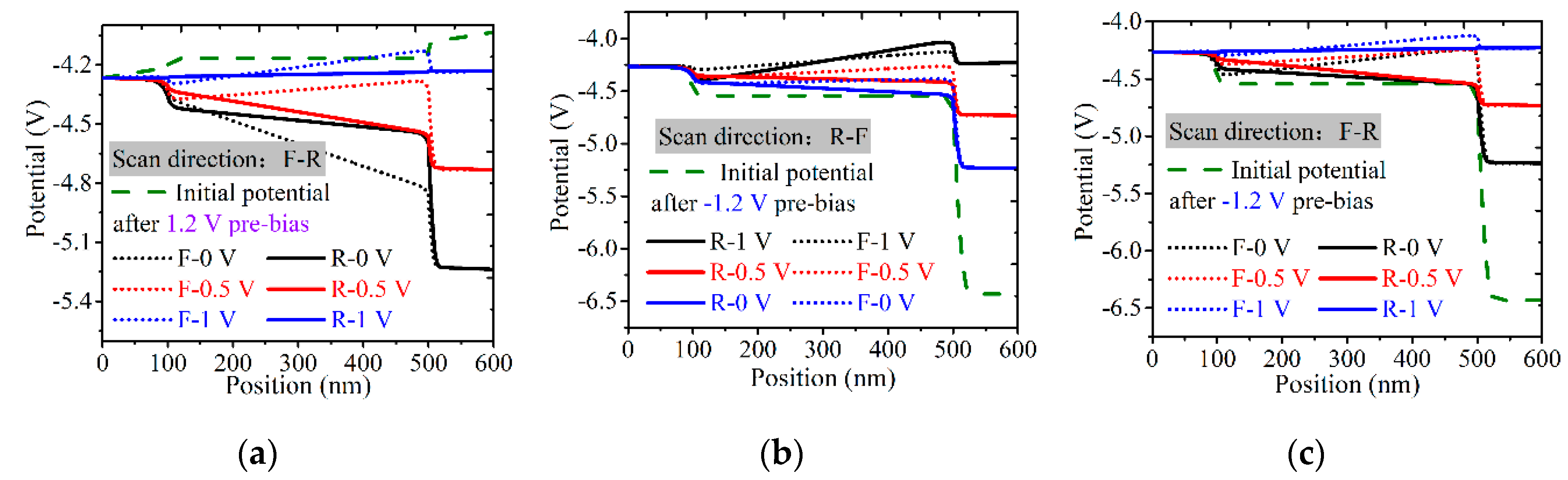
3.2.2. Scan Direction and Pre-Bias Treatment

Scan direction, from reverse to forward (R–F) or from forward to reverse (F–R), combined with a specific voltage pre-bias treatment, has a significant impact on J–V hysteresis according to the experimental reports [30,31]. Here, three different voltages of 1.2, 0 and −1.2 V were adopted for pre-poling the PSC to achieve equilibrated conditions before the J–V test. As seen in Figure 6, we found that the different pre-poling and scan directions could lead to J–V hysteretic loops with varied shapes and extent.
For the scan direction of R–F, we found that the VOC was severely affected by the voltage pre-treatment, while the JSC remained constant. When perovskite solar cells were pre-relaxed by a positive voltage of 1.2 V, the VOC at the reverse scan was the maximum; a bump current density occurred at around R-0.7 V. If the pre-bias voltage decreased, the VOC at reverse scan reduced, and the voltage where the bump current density occurred also reduced. However, when it came to the forward scan, the J–V loops had no serious difference among the three different voltage pre-bias treatment, except that the VOC at forward scan of 1.2 V pre-bias was slightly larger than the other two cases.
For the scan direction of F–R, in contrary to the case of R–F, we found that the JSC was severely affected by the voltage pre-treatment, while the VOC remained constant; the reverse scan curves for the three different voltage pre-bias were almost overlapped with each other, with no obvious difference. However, the forward scan curves were various and complicated. When positive 1.2 V was performed at the pre-bias stage, the obtained forward JSC was even larger than the reverse JSC, and the forward JSC decreased with the decrease in pre-bias voltage. An anomalous forward curve occurred using the negative pre-poling of −1.2 V and obtained a very small JSC of about 4 mA/cm2 with a horrible filling factor and hysteresis.
The corresponding potential profiles for 1.2 and −1.2 V pre-poling are illustrated in Figure 7, and note that the potential profiles for 1.2 V pre-bias with R–F scan is shown in Figure 4a. We could see that for 1.2 V pre-poling, the whole subsequent potential profiles were located below the initial one, while above the initial profile for the cases of −1.2 V pre-poling. This indicates that the positive pre-bias could increase the internal potential of the perovskite solar cells, while the negative pre-bias might reduce the internal potential.
Compared to Figure 4a of R–F scan with 1.2 V pre-poling, the potential profiles for F–R scan showed distinctively downward at the scan step of F-0 V due to the ions’ accumulation during the equilibrium, which could develop a positive electric field to drift the charges flow to the correct transport layers, reducing the recombination and leading to a raised JSC. In the case of −1.2 V pre-equilibrium, the positive ions accumulated at the perovskite/HTL interface and the negative ions at the perovskite/ETL interface, inducing an upward potential profile at the scan step of R-1 V for R–F scan, as seen in Figure 7b. This upward potential induced a negative electric field, prompting the charges to drift to the wrong transport layers, increasing the possibility of recombination, and resulted in the small VOC. The following forward scan steps were similar with the case of 1.2 V pre-poling, the upward potential profiles aggravated the recombination, reducing the current in forward scan and leading to the eventual hysteretic J–V loop. In Figure 7c, for F–R scan with −1.2 V pre-poling, the beginning forward scan steps were all performed under the upward potential profiles, experiencing the extremely severe recombination across the device and inducing to the diminished forward J–V curve.
Above all, changing the scan direction and pre-bias treatment could not improve the solar cell efficiency or suppress J–V hysteresis distinctively. However, the positive pre-bias treatment favored the solar cell photovoltaic performance.

3.3. Materials Improvement to Suppress Hysteresis

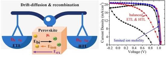
3.3.1. Transport Layers Properties

As discussed above, hysteresis-free J–V curves might be obtained by optimizing the measurement protocols; however, the measurement methods just coped with the superficial issues, and the intrinsic defects inside of the perovskite solar cells were not eliminated. The transport layers have been verified to have a significant effect on J–V hysteresis experimentally and numerically [16,32]. Doping concentration and relative permittivity were chosen to investigate how the transport layers affect the J–V performance in this work. Firstly, the ETL and the HTL were studied independently, as seen in Figure 8. We could see that the J–V curves were a little bit more sensitive to the HTL properties than that of the ETL. For the case of ETL, in Figure 8a, the J–V curves seemed to be similar with each other, except that the forward VOC decreased with the increase in DE and εE; the same as the case of HTL in Figure 8b, with the increase in DH and εH, the forward VOC decreased, and the JSC increased a little bit, while J–V hysteresis was not passivated.
Increasing the doping concentration and the permittivity were supposed to increase the JSC and VOC by enhancing their conductivity and promoting the charge carrier’s transportation, while in contradiction with our calculation results. After carefully analysis, we found that the material properties between the ETL and the HTL were not equal or balanced, and the corresponding conductivities were different. If the conductivity of the ETL or the HTL increases independently, it will aggravate the transport imbalance between the electrons and the holes. In this case, even though the electrons (or holes) could be extracted efficiently, the remaining holes (or electrons) in the perovskite material still promoted the recombination to decrease the photovoltaic performance. It is worth mentioning that the combined effect [16] did not occur in our calculations, that a fixed product (DE · εE) or (DH · εH) could obtain identical J–V curves using different DE, εE, or different DH, εH. Furthermore, this combined effect might need to be verified by a detailed experiment or a more deeply theoretical study, which is beyond the research scope in this work.
Rarely, numerical and experimental research has been focused on the imbalanced transportation between the ETL and the HTL. Here, we attempted to calculate and analyze the influences of the ETL and HTL balance on J–V hysteresis. The parameters used here might be ridiculous for materials design and engineering and just give a preliminary guideline for material selection in PSC, as seen in Figure 9.
Firstly, for the balance of the relative permittivity, a fixed doping concentration of DE = DH = 1024 m−3 was adopted, as seen in Figure 9a, set εE = εH. With the increase in the permittivity, the J–V performance increased, while the extent of hysteresis increased and decreased; the JSC raised gradually, while the VOC decreased and increased. When εE = εH = 0.3, the JSC, VOC and the efficiency were small, although the extent of J–V hysteresis was moderate. When εE = εH = 300, the photovoltaic efficiency enhanced, and J–V hysteresis also could be passivated efficiently. The same results for the balance of doping concentration between the ETL and the HTL were seen in Figure 9b, here, set εE = εH = 30. When DE = DH = 1026 m−3, the efficiency increased, and J–V hysteresis decreased. Therefore, considering the efficiency and the hysteresis, the permittivity and the doping concentration in the ETL and the HTL should be high enough, which is a great challenge to the material research.
Above all, in order to improve the solar cell efficiency and suppress J–V hysteresis, the permittivity and doping properties of the electron and hole transport layers should be balanced and elevated simultaneously, which raises a great challenge to the transport layer materials.

3.3.2. Perovskite Layer Properties

The properties of the perovskite layer are supposed to determine the overall performance of the PSC, working as the light absorbing layer and the mixed electronic-ionic conductor. Since the perovskite material was defined as an intrinsic semiconductor without doping additives, thus, just the permittivity εP was analyzed here. As seen in Figure 10a, the J–V curves present no obvious differences. Thus, our calculation indicated that the permittivity εP was not the primary factor influencing J–V hysteresis, and the charge carrier transportation inside of the perovskite layer was just a representation of the dominant factors—ions’ migration and recombination.
For the defective ions in the perovskite layer, as discussed above, it had been verified to be a necessary element to reproduce hysteretic J–V curves. Here, the ions concentration Di and mobility μi were investigated. The results present that the concentration of the ions had no effect on the J–V loops, as seen in Figure 10b, which indicates the potential of large-area PSC panels for commercialization, but might affect long-term stability due to ion-assisted decomposition [33,34]. For the mobility of ions in the perovskite layer, as seen in Figure 10c, the mobility of ions played a significant role in the hysteretic issue. The very slow-moving ions or the extreme condition with immobile ions, the hysteresis could be eliminated thoroughly. For the case of very high ion mobility, 10−12 m2 V−1 s−1, the ions movement could keep pace with or even faster than the voltage scan rate. The ions accumulated at the corresponding interfaces immediately following with the internal electric field, and no delay or hysteretic current occurred. However, the rapid-changing Eion could prevent the charge carrier’s transportation and deteriorate the recombination, leading to a reduced JSC.
Overall, we proposed that restricting ionic movement is a significant approach to passivate the hysteresis phenomena in the PSCs, requiring a new stabilized perovskite structure and more stable materials, or attempting to block the ions mobile pathway using effective additives.

4. Conclusions

In summary, a mixed electronic-ionic drift-diffusion model combined with the bulk and interfacial recombination was implemented to uncover the nature characteristics of J–V hysteresis in the perovskite solar cells. The model was verified via generating the hysteretic J–V loops with the combined effect of the ion migration and the recombination. The movement and variation of the charges, ions and the electric potential were explored deeply to elucidate the generating principles of J–V hysteresis. The mobile ions could migrate to the interfaces between the perovskite/transport layers, regulating the internal electric potential profiles to influence the charges’ ejection to the transport layers. As long as the charges run out of their lifetimes, the recombination takes place to reduce the charges transportation, leading to a diminished photocurrent. A proper scan rate and a favorable voltage pre-bias poling could really obtain a hysteresis-free J–V curve via alleviating the adverse effect of the ions’ migration and the recombination. A standard measurement protocol is essential to evaluate the perovskite solar cells appropriately. In addition, the balancing of the material properties between the electron transport layer and the hole transport layer significantly influenced J–V hysteresis; combined with the restriction of the ion’s mobility in the perovskite layer, a negligible hysteresis could be achieved, while possibly raising challenges to the new material development. Our work reveals the primary rules underlying J–V hysteresis in perovskite solar cells and provides a preliminary guideline for new material research to eliminate the hysteresis.

Supplementary Materials

The following are available online at https://www.mdpi.com/2304-6732/7/3/47/s1, Mathematical equations, Calculation method, Figure S1: Scan rate determined by a triangle function.

Author Contributions

Conceptualization, C.Y., X.S. and T.X.; methodology, C.Y.; software, C.Y.; validation, C.Y., X.S. and T.X.; formal analysis, C.Y.; investigation, C.Y.; resources, X.S.; data curation, C.Y.; writing—original draft preparation, C.Y.; writing—review and editing, C.Y. and X.S.; visualization, C.Y.; supervision, X.S. and T.X.; project administration, X.S. and T.X.; funding acquisition, X.S. and T.X. All authors have read and agreed to the published version of the manuscript.

Funding

This research was funded by the National Natural Science Foundation of China, grant number 51677043.

Conflicts of Interest

The authors declare no conflict of interest.

References

  1. Liu, X.; Cheng, Y.; Liu, C.; Zhang, T.; Zhang, N.; Zhang, S.; Chen, J.; Xu, Q.; Ouyang, J.; Gong, H. 20.7% highly reproducible inverted planar perovskite solar cells with enhanced fill factor and eliminated hysteresis. Energy Environ. Sci. 2019, 12, 1622–1633. [Google Scholar] [CrossRef]
  2. Min, H.; Kim, M.; Lee, S.U.; Kim, H.; Kim, G.; Choi, K.; Lee, J.H.; Seok, S.I. Efficient, Stable Solar Cells by Using Inherent Bandgap of Alpha-Phase Formamidinium Lead Iodide. Science 2019, 366, 749–753. [Google Scholar] [CrossRef]
  3. NREL. Best Research-Cell Efficiency Chart. Available online: https://www.nrel.gov/pv/cell-efficiency.html (accessed on 6 June 2020).
  4. Kim, D.; Jung, H.J.; Park, I.J.; Larson, B.W.; Dunfield, S.P.; Xiao, C.; Kim, J.; Tong, J.; Boonmongkolras, P.; Ji, S.G.; et al. Efficient, Stable Silicon Tandem Cells Enabled by Anion-Engineered Wide-Bandgap Perovskites. Science 2020, 368, 155–160. [Google Scholar] [CrossRef] [PubMed]
  5. Liu, P.; Wang, W.; Liu, S.; Yang, H.; Shao, Z. Fundamental Understanding of Photocurrent Hysteresis in Perovskite Solar Cells. Adv. Energy Mater. 2019, 9, 1803017. [Google Scholar] [CrossRef]
  6. Jacobs, D.A.; Wu, Y.; Shen, H.; Barugkin, C.; Beck, F.J.; White, T.P.; Weber, K.; Catchpole, K.R. Hysteresis Phenomena in Perovskite Solar Cells: The Many and Varied Effects of Ionic Accumulation. Phys. Chem. Chem. Phys. 2017, 19, 3094–3103. [Google Scholar] [CrossRef] [PubMed] [Green Version]
  7. Chen, S.; Wen, X.; Sheng, R.; Huang, S.; Deng, X.; Green, M.A.; Ho-Baillie, A. Mobile Ion Induced Slow Carrier Dynamics in Organic–Inorganic Perovskite CH3NH3PbBr3. ACS Appl. Mater. Interfaces 2016, 8, 5351–5357. [Google Scholar] [CrossRef] [PubMed]
  8. Chen, B.; Yang, M.; Priya, S.; Zhu, K. Origin of J–V Hysteresis in Perovskite Solar Cells. J. Phys. Chem. Lett. 2016, 7, 905–917. [Google Scholar] [CrossRef]
  9. Van Reenen, S.; Kemerink, M.; Snaith, H.J. Modeling Anomalous Hysteresis in Perovskite Solar Cells. J. Phys. Chem. Lett. 2015, 6, 3808–3814. [Google Scholar] [CrossRef] [Green Version]
  10. Diao, X.-F.; Tang, Y.-L.; Xie, Q.; Chen, D.-L.; Li, S.-X.; Liu, G.-F. Study on the Property of Electron-Transport Layer in the Doped Formamidinium Lead Iodide Perovskite Based on DFT. ACS Omega 2019, 4, 20024–20035. [Google Scholar] [CrossRef]
  11. Eames, C.; Frost, J.M.; Barnes, P.R.; O’regan, B.C.; Walsh, A.; Islam, M.S. Ionic Transport in Hybrid Lead Iodide Perovskite Solar Cells. Nat. Commun. 2015, 6, 7497. [Google Scholar] [CrossRef] [Green Version]
  12. Richardson, G.; O’Kane, S.E.J.; Niemann, R.G.; Peltola, T.A.; Foster, J.M.; Cameron, P.J.; Walker, A.B. Can Slow-Moving Ions Explain Hysteresis in the Current–Voltage Curves of Perovskite Solar Cells? Energy Environ. Sci. 2016, 9, 1476–1485. [Google Scholar] [CrossRef] [Green Version]
  13. Calado, P.; Telford, A.M.; Bryant, D.; Li, X.; Nelson, J.; O’Regan, B.C.; Barnes, P.R.F. Evidence for Ion Migration in Hybrid Perovskite Solar Cells with Minimal Hysteresis. Nat. Commun. 2016, 7, 13831. [Google Scholar] [CrossRef] [PubMed]
  14. Courtier, N.E.; Cave, J.M.; Walker, A.B.; Richardson, G.; Foster, J.M. Ionmonger: A Free and Fast Planar Perovskite Solar Cell Simulator with Coupled Ion Vacancy and Charge Carrier Dynamics. J. Comput. Electron. 2019, 18, 1435–1449. [Google Scholar] [CrossRef] [Green Version]
  15. Courtier, N.E.; Richardson, G.; Foster, J.M. A fast and robust numerical scheme for solving models of charge carrier transport and ion vacancy motion in perovskite solar cells. Appl. Math. Model. 2018, 63, 329–348. [Google Scholar] [CrossRef]
  16. Courtier, N.E.; Cave, J.M.; Foster, J.M.; Walker, A.B.; Richardson, G. How Transport Layer Properties Affect Perovskite Solar Cell Performance: Insights from a Coupled Charge Transport/Ion Migration Model. Energy Environ. Sci. 2019, 12, 396–409. [Google Scholar] [CrossRef] [Green Version]
  17. Shen, H.; Jacobs, D.A.; Wu, Y.; Duong, T.; Peng, J.; Wen, X.; Fu, X.; Karuturi, S.K.; White, T.P.; Weber, K.; et al. Inverted Hysteresis in CH3NH3PbI3 Solar Cells: Role of Stoichiometry and Band Alignment. J. Phys. Chem. Lett. 2017, 8, 2672–2680. [Google Scholar] [CrossRef]
  18. Xiang, J.; Li, Y.; Huang, F.; Zhong, D. Effect of Interfacial Recombination, Bulk Recombination and Carrier Mobility on The J–V Hysteresis Behaviors of Perovskite Solar Cells: A Drift-Diffusion Simulation Study. Phys. Chem. Chem. Phys. 2019, 21, 17836–17845. [Google Scholar] [CrossRef] [PubMed]
  19. Nemnes, G.A.; Besleaga, C.; Tomulescu, A.G.; Palici, A.; Pintilie, L.; Manolescu, A.; Pintilie, I. How Measurement Protocols Influence the Dynamic J-V Characteristics of Perovskite Solar Cells: Theory and Experiment. Sol. Energy 2018, 173, 976–983. [Google Scholar] [CrossRef] [Green Version]
  20. Walter, D.; Fell, A.; Wu, Y.; Duong, T.; Barugkin, C.; Wu, N.; White, T.; Weber, K. Transient Photovoltage in Perovskite Solar Cells: Interaction of Trap-Mediated Recombination and Migration of Multiple Ionic Species. J. Phys. Chem. C 2018, 122, 11270–11281. [Google Scholar] [CrossRef]
  21. Bi, D.; Tress, W.; Dar, M.I.; Gao, P.; Luo, J.; Renevier, C.; Schenk, K.; Abate, A.; Giordano, F.; Baena, J.-P.C. Efficient Luminescent Solar Cells Based on Tailored Mixed-Cation Perovskites. Sci. Adv. 2016, 2, e1501170. [Google Scholar] [CrossRef] [Green Version]
  22. Wang, Z.; Lin, Q.; Wenger, B.; Christoforo, M.G.; Lin, Y.-H.; Klug, M.T.; Johnston, M.B.; Herz, L.M.; Snaith, H.J. High Irradiance Performance of Metal Halide Perovskites for Concentrator Photovoltaics. Nat. Energy 2018, 3, 855. [Google Scholar] [CrossRef]
  23. Foster, J.M.; Snaith, H.J.; Leijtens, T.; Richardson, G. A model for the operation of perovskite based hybrid solar cells: Formulation, analysis, and comparison to experiment. SIAM J. Appl. Math. 2014, 74, 1935–1966. [Google Scholar] [CrossRef]
  24. Yin, W.-J.; Yang, J.-H.; Kang, J.; Yan, Y.; Wei, S.-H. Halide perovskite materials for solar cells: A theoretical review. J. Mater. Chem. A 2015, 3, 8926–8942. [Google Scholar] [CrossRef]
  25. Rong, Y.; Hu, Y.; Ravishankar, S.; Liu, H.; Hou, X.; Sheng, Y.; Mei, A.; Wang, Q.; Li, D.; Xu, M. Tunable Hysteresis Effect for Perovskite Solar Cells. Energy Environ. Sci. 2017, 10, 2383–2391. [Google Scholar] [CrossRef]
  26. Peng, J.; Wu, Y.; Ye, W.; Jacobs, D.A.; Shen, H.; Fu, X.; Wan, Y.; Duong, T.; Wu, N.; Barugkin, C.; et al. Interface Passivation Using Ultrathin Polymer-Fullerene Films for High-Efficiency Perovskite Solar Cells with Negligible Hysteresis. Energy Environ. Sci. 2017, 10, 1792–1800. [Google Scholar] [CrossRef] [Green Version]
  27. Shao, Y.; Xiao, Z.; Bi, C.; Yuan, Y.; Huang, J. Origin and Elimination of Photocurrent Hysteresis by Fullerene Passivation in CH3NH3PbI3 Planar Heterojunction Solar Cells. Nat. Commun. 2014, 5, 5784. [Google Scholar] [CrossRef]
  28. Snaith, H.J.; Abate, A.; Ball, J.M.; Eperon, G.E.; Leijtens, T.; Noel, N.K.; Stranks, S.D.; Wang, J.T.-W.; Wojciechowski, K.; Zhang, W. Anomalous Hysteresis in Perovskite Solar Cells. J. Phys. Chem. Lett. 2014, 5, 1511–1515. [Google Scholar] [CrossRef]
  29. Tress, W.; Marinova, N.; Moehl, T.; Zakeeruddin, S.; Nazeeruddin, M.K.; Grätzel, M. Understanding the Rate-Dependent J–V Hysteresis, Slow Time Component, and Aging in CH3NH3PbI3 Perovskite Solar Cells: The Role of a Compensated Electric Field. Energy Environ. Sci. 2015, 8, 995–1004. [Google Scholar] [CrossRef]
  30. Bruno, A.; Cortecchia, D.; Chin, X.Y.; Fu, K.; Boix, P.P.; Mhaisalkar, S.; Soci, C. Temperature and Electrical Poling Effects on Ionic Motion in MAPbI3 Photovoltaic Cells. Adv. Energy Mater. 2017, 7, 1700265. [Google Scholar] [CrossRef]
  31. Anghel, D.V.; Nemnes, G.A.; Pintilie, I.; Manolescu, A. Modelling J–V Hysteresis in Perovskite Solar Cells Induced by Voltage Poling. Phys. Scr. 2019, 94, 125809. [Google Scholar] [CrossRef]
  32. Cai, F.; Yang, L.; Yan, Y.; Zhang, J.; Qin, F.; Liu, D.; Cheng, Y.-B.; Zhou, Y.; Wang, T. Eliminated Hysteresis and Stabilized Power Output over 20% in Planar Heterojunction Perovskite Solar Cells by Compositional and Surface Modifications to the Low-Temperature-Processed TiO2 Layer. J. Mater. Chem. A 2017, 5, 9402–9411. [Google Scholar] [CrossRef]
  33. Correa-Baena, J.-P.; Saliba, M.; Buonassisi, T.; Grätzel, M.; Abate, A.; Tress, W.; Hagfeldt, A. Promises and challenges of perovskite solar cells. Science 2017, 358, 739–744. [Google Scholar] [CrossRef] [PubMed] [Green Version]
  34. Park, N.-G.; Grätzel, M.; Miyasaka, T.; Zhu, K.; Emery, K. Towards stable and commercially available perovskite solar cells. Nat. Energy 2016, 1, 16152. [Google Scholar] [CrossRef]
Figure 1. Schematic of the (a) working principle and the corresponding (b) calculation model of the perovskite solar cell (PSC). The ions and charge carriers were equilibrated at 1.2 V in the light, and their movement and transportation are indicated with the arrows.
Photonics 07 00047 g001
Figure 2. Influences of the defective ions and various recombinations on J–V hysteresis curves. (a) J–V hysteresis calculation with (Yes) or without (No) ions and recombination (Rec); (b,c) different hysteresis loops with various combos of the bulk (Rbulk) and the interfacial (RETL, RHTL) recombination.
Photonics 07 00047 g002
Figure 3. Schematic of the transformation of the charge carriers, defective ions and electric field during the J–V measurement from reverse to forward (R–F, from 1.2 to −0.2 to 1.2 V) after 1.2 V pre-bias poling, including Rbulk, RETL and RHTL. (a) Reverse-1 (R-1) V; (b) Reverse-0.5 (R-0.5) V and Reverse-0 (R-0) V; and (c) Forward-0 (F-0) V, Forward-0.5 (F-0.5) V and Forward-1 (F-1) V.
Photonics 07 00047 g003
Figure 4. (a) Variation of the electrical potential profile and (b) the corresponding concentration difference between the negative ions N and the positive ions P during reverse scan (R) and forward scan (F), including ions migration (Ions) and recombination (Rec).
Photonics 07 00047 g004
Figure 5. Influences of scan rates on (a) J–V hysteresis; (b,c) potential profiles at the scan rate of 2.4 V/s and 4 mV/s, respectively.
Photonics 07 00047 g005
Figure 6. Influences of the voltage pre-bias and the scan direction on J–V hysteresis. (a) Scan direction from reverse to forward (R–F); and (b) scan direction from forward to reverse (F–R).
Photonics 07 00047 g006
Figure 7. Potential profiles corresponding to the cases in Figure 6. (a) 1.2 V pre-poling, scan direction of F–R; −1.2 V pre-bias treatment for (b) R–F scan and (c) F–R scan. Note that the potential profiles for 1.2 V pre-bias with R–F scan is shown in Figure 4a.
Photonics 07 00047 g007
Figure 8. Effects of the doping concentrations DE and DH and the relative permittivity εE and εH of (a) ETL and (b) HTL on J–V hysteresis.
Photonics 07 00047 g008
Figure 9. Effects of the materials properties balance on J–V hysteresis. (a) The balance of εE and εH; (b) the balance of DE and DH.
Photonics 07 00047 g009
Figure 10. Influences of the properties in the perovskite layer on J–V hysteresis. (a) The relative permittivity εP; (b) the concentration (Di) and (c) the mobility (μi) of the ions.
Photonics 07 00047 g010
Table 1. Material parameters adopted in model definition.
ParametersETL(E)Perovskite(P)HTL(H)Reference
Permittivity εE,P,H31183[13,18,20,23]
Bandgap Eg (eV)31.63.2[13,16,18]
Doping concentration DE,H (m−3)1024——1024[13,16,25]
Effective density of state in conduction band NC (m−3)10265 × 10241026[18]
Effective density of state in valence band NV (m−3)10265 × 10241026[18]
Electron affinity (eV)4.153.952.15[13,20]
Electron mobility μn (m2/(V∙s))10−82 × 10−410−8[13,20]
Hole mobility μp (m2/(V∙s))10−82 × 10−410−8[13,20]
Ion concentration Di (m−3)——5 × 10²³——[13,16]
Ion mobility μi (m2/(V∙s))——10−14——[13,16]

