1. Introduction
The physical scaling of transistors and the enhancement of their integration degree have remained the primary trends of integrated electronics for many years. Until recently, the extensive development of integrated circuits (ICs) provided the steady improvement of computer system performance and the fulfillment of Moore’s law [
1]. Nowadays, the growth is considerably slowing down, because the semiconductor industry is approaching the fundamental limits of traditional microelectronic principles. The transition to nanometer feature dimensions of transistors is ongoing, and this process results in multiple technological, architectural, and design challenges.
Traditional techniques of on-chip and chip-to-chip interconnecting are based on the application of metal conductors, which transmit signals by the charging and discharging of the whole wire. The degradation of metal interconnection characteristics in ultra-large-scale ICs (ULSIs) and other innovative integrated devices is an urgent scaling-related problem [
2,
3]. On the one hand, the downscaling of transistors leads to the miniaturization and more dense packing of local- and intermediate-level wires in ULSIs and to the reduction in metallization step. On the other hand, the increase in chip area elongates global-level links between IC components, e.g., inter-core connections in multi-core microprocessors. Both tendencies, together with the operation frequency boost, determine the rise in parasitic capacitance and resistance of on-chip metal conductors and the dramatic deterioration of their response time, channel capacity, energy efficiency, noise immunity, reliability, and other vital parameters. Moreover, the insufficient properties of long inter-chip metal wires at high rates of data transmission affect the performance of multi-chip systems.
To overcome the restrictions of metal conductors, novel methods of IC interconnecting are proposed [
4,
5,
6,
7,
8]. Some of them address the further modification and optimization of traditional techniques based on multi-level metal links (e.g., circuit methods, new conducting alloys, length minimization, three-dimensional design). The most promising methods suppose the implementation of fundamentally new interconnection types (e.g., wireless networks on chip, super- and nanoconductors, graphene, carbon nanotube and optical links). It is expected that they will provide further development of integrated electronics and the creation of next-generation devices.
An optoelectronic approach considers optical links as an alternative decision for high-performance interconnecting of IC elements and components [
6,
8,
9,
10,
11]. This approach can provide the appreciable advancement of IC characteristics in the immediate future. In addition, it has important geometrical, design, parametric, and technological advantages over its counterparts. However, the efficient implementation of mass-produced integrated devices with optical interconnections requires the solution of some challenges.
In contrast to a simple metal wire, an optical interconnection is a much more complicated system that includes at least four parametrically and technologically matched devices: An integrated or an external source of optical radiation, a high-speed modulator, an integrated waveguide, and a photodetector. At the current stage of the industry, the aforementioned optoelectronic devices have relatively large scales in comparison with state-of-the-art transistors. Consequently, optical interconnections are suitable for the replacement of only global-level on-chip wires and long chip-to-chip connections. The realization of optical links for lower levels of IC hierarchy necessitates the further downscaling of optoelectronic devices to nanometer dimensions.
The processing compatibility of optical links with the central electronic part of IC is the most pressing issue in the field of optical interconnecting. Silicon is a primary material of modern ICs that provides excellent adaptability to streamlined manufacture and small optical losses. Still, the production of available on-chip silicon lasers seems to be very problematic. That is why the methods of heterogeneous integration [
12] and A
IIIB
V-on-silicon techniques [
13] are being researched actively.
Previously, we proposed the concept of on-chip optical interconnections based on original optoelectronic devices that combine the functions of lasers and optical modulators in unified A
IIIB
V semiconductor heterostructures [
14]. These devices are called lasers-modulators and contain transverse control nanoheterostructures with custom profiles of conduction band bottom and valence band top [
15,
16,
17,
18]. The intensity or wavelength of laser radiation is altered through the change in the transverse electric field of the modulator heterostructure. Since the pumping current is constant during the operation, slow transients in the power circuit do not limit the peak modulation frequency of the laser-modulator. The device performance is determined only by subpicosecond processes of carrier relocation between specially organized quantum wells in the bands of the control heterostructure. The maximal modulation frequency of the lasers-modulators reaches the value of 1 THz and above.
This paper regards the development of high-speed optical sensors designed for the detection of short laser pulses generated by the lasers-modulators. It is assumed that both devices are the parts of on-chip optical interconnections and are monolithically integrated with each other and with electronic elements of IC. Photodetectors are characterized by multiple important parameters, such as response time, dark current, nonlinearity, noise equivalent power, linear dynamic range, photoresponsivity, detectivity etc. In this research, we concentrate only on the achievement of subpicosecond response time and technological compatibility with the lasers-modulators. Other parameters are less critical for the realization of laser-modulator-based on-chip optical interconnections, and it is possible to vary them in sufficiently wide ranges.
Drift-diffusion numerical simulation of conventional on-chip
p-
i-
n, Schottky barrier and uni-travelling carrier (UTC) photodetectors demonstrated that their response time is restricted by semiclassical transport effects in A
IIIB
V semiconductor materials and exceeds several picoseconds for the most efficient structures [
17,
19,
20,
21]. Such performance is not sufficient for the adequate detection of short optical pulses generated by the lasers-modulators.
Presently, various novel approaches to the boost of photodetector performance and efficiency are proposed. Photonics and plasmonics offer new possibilities for the creation of advanced photosensitive devices [
22,
23,
24,
25]. The promising variants of light sensing structures demonstrate low dark current, high responsivity and detectivity. However, the monolithic integration of such photodetectors with the A
IIIB
V lasers-modulators cause multiple technological and design issues. Their construction methods are not aimed at the response time decrease and exploit slow-response physical process (e.g., avalanche carrier multiplication in paper [
24]).
Another important research line treats the application of photosensitive resonant tunneling structures [
26,
27,
28]. A resonant tunneling diode (RTDs) has outstanding response speed characteristics, but typical RTD-based photodetectors are characterized by the external configuration of absorption region with respect to a quantum well nanoheterostructure, due to their microwave applications. It is difficult to provide an efficient optical generation directly in RTD regions, and the considered structures have insufficient reproducibility of parameters for the implementation of multiple sensors in mass-produced ULSI chips.
In papers [
29,
30], metal-semiconductor-metal (MSM) and photoconducting devices are discussed. Special processing techniques are used for the carrier lifetime-reduction in active regions of these photodetectors. Though, the modification of semiconductor layers leads to the following adverse effect. At the same time, with recombination rate improvement, carrier mobility is significantly decreased. Electrons and holes are located in modified regions all the time during the detection process. It results in lower sensitivity of photodetectors and more durable transit time of photogenerated charge carriers between contacts.
Therefore, the development of laser-modulator-compatible AIIIBV photodetectors with subpicosecond response time is a relevant research direction. This paper introduces the concept of a novel high-speed AIIIBV photodetector that utilizes the principle of controlled relocation of carrier density peaks within spatially arranged quantum wells for the improvement of back-edge performance. To estimate the response time of the device, we develop and implement a numerical model that combines the semiclassical current density formula and the quantum-mechanical Schrodinger-Poisson equation system.
2. Photodetector with Controlled Relocation of Carrier Density Peaks
In general, the high-speed performance of standard semiconductor photodetectors is influenced by a time of charge carrier transport through the whole device structure and by a resistor-capacitor (RC) time constant [
31,
32]. The transit time of photogenerated charge carriers includes two components: The fast one caused by the drift motion in a depletion region and the slow one determined by the electron and hole diffusion in neutral regions. The RC constant of photodetectors depends on the equivalent capacity of its
p-
n and Schottky-barrier junctions, internal and load resistances. The ways of the transit time reduction are of our main interest in this paper. The RC time shortening, by contrast, represents a technical problem that can be solved by well-known circuit methods.
On-chip A
IIIB
V photodetectors are characterized by quite strong built-in electric fields centered in their active regions [
15,
19,
33]. Hence, the high-field effects of drift velocity saturation and electron inter-valley transition restrict the times of electron and hole transport through a depletion layer. The elimination of the considered effects without the significant modification of design principles or photodetector materials seems to be very problematic. For example, the narrowing of an absorption region does not lead to a visible improvement of the transit time, because the capacitance and RC constant of a photodetector is increased.
The response time of on-chip photodetectors is affected not only by high-field transport properties of A
IIIB
V semiconductors, but also by durable lifetimes of non-equilibrium electrons and holes [
21]. Low recombination rate of photogenerated electron-hole pairs in an absorption region induces a notable delaying of the photocurrent back edge. In conventional photodetector materials, the lifetime of charge carriers exceeds 100 ps. However, it is possible to update the device design in order to improve the lifetime characteristic. For this purpose, low-temperature-grown epitaxial layers (LT layers) are used. The formation of semiconductor layers by the molecular beam epitaxy under low-temperature conditions (less than 500 °C for GaAs) results in dramatically shorter carrier lifetime (about several picoseconds and less) as compared to regular-temperature-grown materials [
34,
35,
36]. The phenomenon of lifetime-reduction is caused by a very high density of defects that act as traps for non-equilibrium electrons and holes. At the same time, the unique structural properties of LT layers determine the considerable decrease in carrier mobility to the values in the range of 100–1000 cm
2/(V·s). This feature poses the major challenge of LT layer utilization in high-speed photosensitive devices. The decline in electron and hole mobilities leads to the appreciable degradation of photodetector transit time, sensitivity and quantum efficiency. To deal with the challenge, advanced techniques of epitaxial growth and custom device configurations are being investigated [
34].
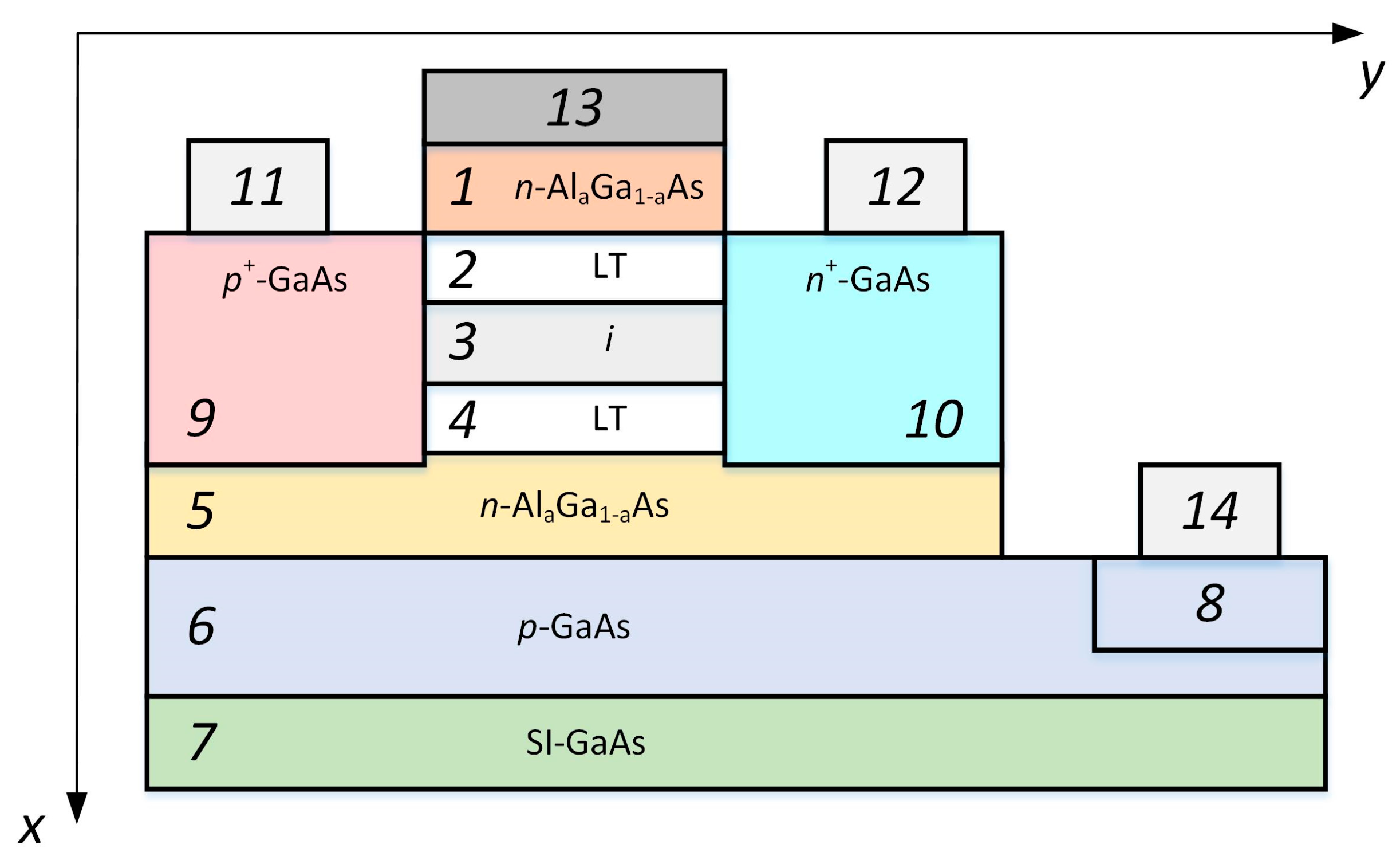
In this paper, we propose a novel design of A
IIIB
V on-chip photodetector with LT layers and a transverse control heterostructure. The overall cross-section of the device is shown in
Figure 1. A heavily doped
p+-GaAs region (Position 9), a thin
i-type
absorbing region (Position 3), and a heavily doped
n+-GaAs region (Position 10) form a photosensitive
p-
i-
n structure. The photon energy of detected laser pulses corresponds to the bandgap energy of the absorbing region (Position 3). In other regions of the photodetector, bandgap energy exceeds the photon energy of incident light, and the optical generation of electron-hole pairs does not occur. The direction of light propagation is normal to the plane of cross-section. Such configuration allows for creation of a Fabri-Perot optical resonant cavity that provides high quantum efficiency at small dimensions of the device regions along
x and
y axes.
The photosensitive
p-
i-
n heterojunction (Positions 9, 3 and 10 in
Figure 1) operates in the standard photodiode mode. A constant bias voltage of reverse polarity is applied to supply ohmic contacts (Positions 11 and 12), which are connected with the heavily doped
p+- and
n+-GaAs regions (Positions 9 and 10). During the device illumination by optical radiation with sufficient photon energy, non-equilibrium electrons and holes are generated in the absorbing region (Position 3). The built-in electric field of the
p-
i-
n structure is directed along the
y axis. It divides photogenerated charge carriers and relocates them through the depletion layer to the heavily doped
p+ and
n+ regions (Positions 9 and 10). When electrons and holes reach the supply contacts, they flow through the supply circuit and generate photocurrent. This photocurrent is a measuring signal of the photodetector.
If an LT layer acts as the active region of a photodetector, short carrier lifetime and low mobility impair the device sensitivity and transit time. To avoid this negative impact, we utilize a principle of controlled relocation of carrier density peaks [
37,
38,
39]. According to the principle, the fast shifting of electrons and holes between specially arranged quantum regions of nanoheterostructure under the influence of the transverse electric field improves the high-speed performance of semiconductor devices.
In contrast to conventional
p-
i-
n photodiodes, the photodetector with controlled relocation of carrier density peaks includes the control heterostructure. It is formed by an upper Schottky-barrier control junction with an
n-
region and a metal layer (Positions 1 and 13 in
Figure 1), an upper LT-
layer (Position 2), the
i-
absorbing region (Position 3), a lower LT-
layer (Position 4), and a lower
p-
n control junction with an
n-
and a
p-GaAs regions (Positions 5 and 6). A control bias voltage is applied to Schottky and ohmic control contacts (Positions 13 and 14). The transverse electric field induced by the control voltage is normal to the
p-
i-
n structure field and is directed along the
x axis.
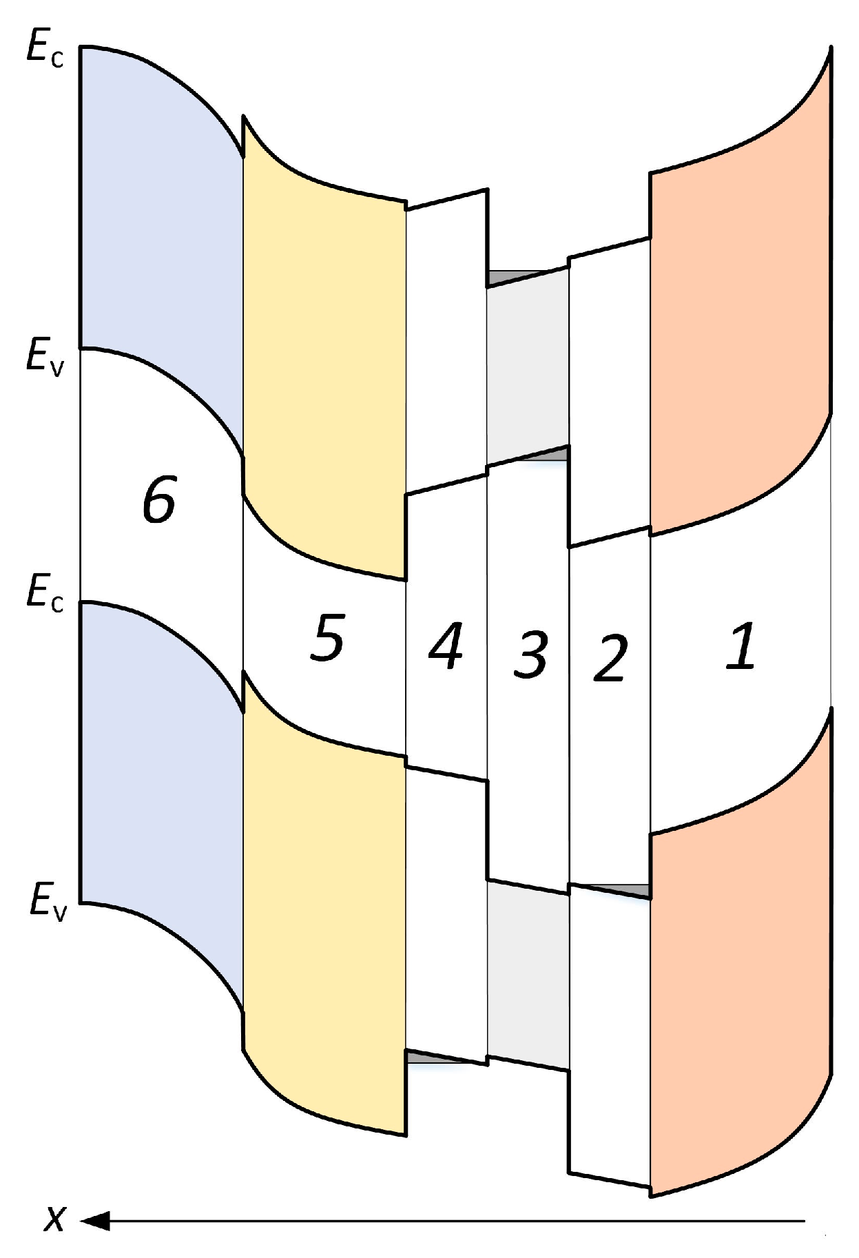
Energy band diagrams of the control heterostructure for different values of the control voltage are given in
Figure 2. Heterojunctions create potential barriers for holes in the valence band (between regions 3 and 2, 4 and 5) and for electrons in the conduction band (between regions 3 and 4, 2 and 1). The barriers prevent the intensive leakage of photogenerated carriers to the control circuit. If the control voltage equals to zero (in some cases, non-zero initial bias voltage can be used), the maximums of electron and hole densities are overlapped in the thin absorbing region (Position 3) with slow recombination rate and high carrier mobility (see the upper diagram in
Figure 2). Therefore, the photodetector operates analogously to traditional reverse-biased
p-
i-
n photodetectors without LT layers.
Under the influence of bias control voltage, the energy band diagram of the control heterostructure is changed (see the lower diagram in
Figure 2). The transverse electric field divides the peaks of electron and hole densities and relocates them to the recombinational LT layers (Positions 2 and 4). The mentioned layers are characterized by shorter carrier lifetime and lower carrier mobility as compared to the absorbing region (Position 3). The field-controlled relocation takes concise time (less than 0.1 ps), and the total number of charge carriers in quantum wells remains nearly unchanged during this rapid process. The subpicosecond transfer of photogenerated electrons and holes from the absorbing region (Position 3) with high carrier mobility and low recombination rate to the LT layers (Positions 2 and 4) with low mobility and high recombination rate yields the sudden decrease in photocurrent flowing through the supply circuit of the photodetector. The absorbing region (Position 3) has a thickness of about 10 nanometers and less (along
x axis). That is why high-field transport effects in A
IIIB
V materials do not exert intense action on carrier transit time in the transverse direction.
It is advantageous to activate the addressed mechanism of carrier mobility and lifetime modulation only during the back edge of an optical pulse. If the control heterostructure is biased during the whole detection cycle, the rapid decrease in photocurrent after the end of illumination is not observed. Non-equilibrium charge carriers always penetrate the LT layers (Positions 2 and 4 in
Figure 2), and this effect leads to the weakening of concentration jump in the layers triggered by the illumination shutdown. For this reason, the photodetector with controlled relocation of carrier density peaks operates in the following mode. During the leading edge of an optical pulse, the control heterostructure is unbiased, and the device acts as a typical
p-
i-
n photodiode. When the back edge starts, a special circuit generates the constant bias voltage at the control contacts (Positions 13 and 14 in
Figure 1), and the relocation process is launched.
The photodetectors with controlled relocation of carrier density peaks are designed for the functioning as parts of on-chip optical interconnections together with the lasers-modulators. To provide the specific operation mode with a variable control voltage, the transmitted digital electric signal is converted to short laser pulses with the fixed duration of
. A high-speed circuit drives the device, based on advanced logic elements with controlled relocation of wavefunction amplitude maximums [
16]. In the initial state, after the end of supply transient, the control voltage equals zero. Photocurrent flowing through the supply circuit activates the control circuit, and it applies the bias voltage to the control contacts (Positions 13 and 14 in
Figure 1). The reaction time of the control circuit exactly matches
parameter, and the voltage appearance coincides with the start of the pulse back edge. The emergence of the transverse electric field results in the relocation of carrier density peaks from the absorbing region (Position 3) to the recombinational LT layers (Positions 2 and 4) and in the corresponding photocurrent decrease. When the relocation and recombination are finished, the control circuit resets the bias of the control heterostructure to zero, and the device is ready for the next pulse detection.
Thus, the photodetector with controlled relocation of carrier density peaks combines the photosensitive p-i-n junction with the orthogonally oriented control heterostructure. The subpicosecond relocation process allows for the improvement of back-edge performance on the retention of high sensitivity and quantum efficiency. To estimate the relocation time that defines the steep section of the photocurrent back edge, the implementation of a quantum-mechanical numerical model is necessary.
3. Numerical Model
In this research, we propose the numerical model of the photodetector with controlled relocation of carrier density peaks. It is necessary for the enhanced estimation of the photocurrent back edge with regard to the features of controlled transverse relocation of charge carrier wavefunctions in the quantum-well regions of the control nanoheterostructure.
On the one hand, the transverse controlled relocation of electrons and holes along the
x axis (see
Figure 1 and
Figure 2) is a quantum-mechanical process that requires the quantum-mechanical approach to simulation [
40,
41]. On the other hand, the photocurrent flow is determined by the semiclassical transport of photogenerated charge carriers in the longitudinal direction along the
y axis. Therefore, we develop the combined model, which addresses the transverse quantum-mechanical transport forced by the control electric field independently from the longitudinal semiclassical transport influenced by the electric field of the
p-
i-
n structure. The proposed model is primarily quantum-mechanical, and semiclassical effects are described approximately.
The quantum-mechanical component of the combined model for the photodetector with controlled relocation of carrier density peaks includes the one-dimensional time-domain Schrodinger-Poisson equation system [
40,
42,
43] solved along the
x axis. We treat the effective mass approximation and assume that the lattice temperature is time- and coordinate-constant. The basic quantum-mechanical equations of the model are formulated as follows:
where
x is the transverse coordinate (see
Figure 1 and
Figure 2);
t is time;
j is the imaginary unit number;
,
are the electron and hole concentrations obtained by the self-consistent solution of the Schrodinger-Poisson Equation system (1)–(5) without due regard to carrier recombination and transport along the
y axis (see
Figure 1 and
Figure 2);
q is the elementary electric charge;
,
are the electron and hole effective masses;
k is the Boltzmann constant;
T is the lattice absolute temperature;
is the Dirac constant;
is the index number of electron resonance level in conduction band;
is the index number of hole resonance level in valence band;
,
are the heterostructure potentials in conduction and valence bands;
is the electrostatic potential;
,
are the time-domain electron and hole wavefunctions;
is the permittivity of a semiconductor;
is the permittivity constant;
,
are the concentrations of ionized donors and acceptors;
,
are the quasi-Fermi levels for electrons and holes;
is the energy of electron resonance level in the conduction band;
is the energy of hole resonance level in the valence band.
The semiclassical part of the combined model for the photodetector with controlled relocation of carrier density peaks consists of the following equations [
44,
45]:
where
is the density of photocurrent, which flows through the supply contacts of the device (see
Figure 1, Positions 11 and 12);
is the magnitude of the supply voltage;
L is the active region length along the
y axis;
H is the total height of the absorbing region (Position 3) and LT layers (Positions 2 and 4) along the
x axis;
,
are the electron and hole mobilities;
n,
p are the electron and hole densities refined with regard to longitudinal transport and recombination;
,
are the electron and hole lifetimes;
,
are the times of electron and hole longitudinal transit along the
y axis. In Equation (6), we take into account the drift motion of charge carriers along the
y axis forced by the intense electric field in the
p-
i-
n structure, but the electron and hole diffusion processes are neglected. Equations (7) and (8) describe the dynamics of carrier density declining because of recombination and longitudinal transport. Carrier mobilities
and
in Equation (6) are calculated using the analytical high-field models represented in [
46].
Equation (6) defines photocurrent density as a product of the specific conductivity (averaged along the x axis) and the transverse component of electric field intensity (averaged along the y axis). The model supposes a two-step calculation of spatial and time distributions for carrier densities. Firstly, we compute quantum-mechanical carrier densities and by the self-consistent solution of the Schrodinger-Poisson Equation system (1–5). At this step, finite difference coordinate and time grids are used, and the processes of carrier recombination and transport along the y axis are not taken into account. Secondly, we refine concentrations n and p with regard to carrier lifetimes , in the heterostructure layers and to time intervals , of electron and hole high-field transit along the y axis. The processes mentioned above determine the decrease in the densities of non-equilibrium photogenerated electrons and holes during the back edge of a photocurrent pulse.
At the control contacts of the photodetector with controlled relocation of carrier density peaks (coordinate grid points
and
), we set the following first-type boundary conditions for the Schrodinger Equations (1), (2) and the Poisson Equation (5):
where
is the coordinate of a contact;
is the intrinsic charge carrier concentration;
is the contact potential difference of the corresponding junction;
is the control voltage applied to a junction. To simplify the statement of boundary conditions for electron and hole wavefunctions, we assume that the photodetector has two Schottky-barrier control junctions. It is a feasible assumption because the types of control junctions do not affect the device efficiency.
For the calculation of initial conditions (energy levels and wavefunctions of electrons and holes, spatial distributions of electrostatic potential and carrier densities), we solve the full stationary problem numerically. In the stationary case, the Schrodinger Equations (1) and (2) take the following form:
where
,
are the envelopes of electron and hole wavefunctions. Other equations of the Schrodinger-Poisson system and boundary conditions remain unchanged, but we substitute
and
instead of time-domain wavefunctions
and
.
In numerical models of semiconductor photosensitive devices, the influence of illumination on their characteristics is typically described through the bipolar optical generation rate
[
17,
19]. This paper is focused on the back-edge performance of the photodetector with controlled relocation of carrier density peaks. Hence, it is necessary to take
into account only during the calculation of initial conditions, which correspond to the stationary state after the end of illumination transient. However, Model (1)–(12) does not include
as a simulation parameter. To solve this issue, we propose the following approach.
There are high concentrations of photogenerated electrons and holes in the absorbing region of the photodetector before the beginning of the optical pulse’s back edge. For the consideration of this feature, we set a specific difference between the electron and hole quasi-Fermi levels during the calculation of initial conditions. The relations between quantities , and , are given by Equations (3), (4), (7) and (8). When we solve the time-domain problem, spatial distributions of quasi-Fermi levels and corresponding carrier concentrations are refined iteratively for each point of time grid. Using the proposed approach, one can describe the redistribution of photogenerated charge carriers under the influence of a built-in electric field.
It is possible to obtain the simplified ratio between the optical radiation and resonant cavity parameters and non-equilibrium electron density
in the absorbing region of the photodetector at the initial time of the simulation. The bipolar optical generation rate
is given as follows [
17,
19]:
where
is the input power of an optical pulse;
is the external quantum efficiency of the photodetector, which depends on the reflection coefficients of resonant cavity mirrors, resonator length, and absorption coefficient;
is the resonant cavity volume;
is the photon energy or the bandgap energy in the absorbing region of the photodetector. Due to the stationary state, carrier generation is almost balanced by the recombination process. Consequently, the following approximate expression is valid:
One can use Formula (14) for the estimation of input optical power that corresponds to certain resonant cavity configuration and initial electron concentration in the absorbing region.
Thus, we developed the combined numerical model of the photodetector with controlled relocation of carrier density peaks that includes the Schrodinger-Poisson Equation systems (1)–(5), semiclassical transport Equations (6)–(8), boundary Conditions (9), (10), and initial conditions derived from the numerical solution of the stationary Schrodinger-Poisson equation system. Supplementary Formula (14) associates non-equilibrium carrier concentration in the absorbing region of the photodetector with the input optical power and parameters of the resonant cavity.
4. Simulation Technique
The implementation of the combined model in Equations (1)–(8) requires the utilization of a numerical simulation technique, which consists of an efficient discretization method and a high-performance computational algorithm. Nowadays, multiple software packages enable the numerical computer-aided solution of the Schrodinger-Poisson equation system [
47,
48]. However, many features of the model realization are user-transparent in these standard tools. Also, the range of available materials and device configurations is limited, and the simulation of specific or novel devices necessitates a significant code revision. That is why we develop our simulation technique and the appropriate applied software in this research.
In order to reduce a computational error, we perform the scaling of the model’s equations. Then, we solved normalized equations by the finite difference numerical method [
49] using the following coordinate, time, and carrier energy grids
,
, and
:
where
I,
M,
R are the numbers of grid points by coordinate, by time, and by the energy of charge carriers, respectively.
We apply two different systems of scaling factors. The first system given in
Table 1 is designed for the normalization of the Schrodinger Equations (1), (2), and wavefunction boundary Condition (9). The second system represented in
Table 2 is employed for the Poisson Equation (5) and potential boundary Condition (10). Equations (3), (4), (6)–(8) are not scaled. The suggested approach reduces all physical constants in the Schrodinger and Poisson equations, but the normalization and denormalization procedures are carried out during each iteration of numerical calculations.
Time-domain discretization scheme of the model’s equations is based on the implicit numerical method [
50]. After the scaling by factors given in
Table 1 and
Table 2, time and spatial discretization, non-stationary Equations (1)–(8) takes the following form:
where
i,
m are the indexes of coordinate and time grids according to (15) and (16);
is the time grid step;
is the coordinate grid step.
The stationary finite difference formulation of the normalized Schrodinger-Poisson equation system is given as follows:
For the calculation of initial conditions through the stationary problem solution, we apply the following numerical algorithm:
Declare input data.
Specify the permissible value of computing residual .
Generate coordinate and energy grids and according to Formulas (15) and (17). Define grid functions of time-independent parameters , , , , , , , , , , , and .
Set and , where k, l are the loop iterators. Specify initial approximations , , , and .
Scale and solve Equations (26) and (27) numerically, obtain , , , and . Denormalize the quantities.
Compute carrier densities and using Formulas (28) and (29).
Define spatial distributions of electron and hole mobilities and .
Refine spatial distributions of quasi-Fermi levels and .
Calculate residual .
If , set , and go back to Step 6. Otherwise, go to Step 11.
Scale and solve Equation (30) numerically, obtain . Denormalize the quantities.
Compute residual .
If , set , and go back to Step 5. Otherwise, the initial conditions for time-domain simulation are obtained.
To perform the time-domain simulation of the photodetector with controlled relocation of carrier density peaks, we propose the following numerical algorithm:
Load initial conditions.
Generate a time grid according to Formula (16).
Set , , and , where m is the time loop iterator.
Scale and solve Equations (18) and (19) numerically, obtain and . Denormalize the quantities.
Compute carrier densities and from Formulas (20) and (21).
Define spatial distributions of electron and hole mobilities and .
Refine spatial distributions of quasi-Fermi levels and .
Calculate residual .
If , set , and go back to Step 5. Otherwise, go to Step 10.
Scale and solve Equation (22) numerically, obtain . Denormalize the quantities.
Compute residual .
If , set , and go back to Step 4. Otherwise, go to Step 13.
Calculate carrier densities and using Equations (24) and (25).
Estimate photocurrent density as provided by Formula (23).
If , where M is the last point of time grid, output the results of time-domain numerical simulation. Otherwise, set , and go back to Step 4.
Thus, we developed the numerical simulation technique suitable for the realization of the Model (1)–(8) for the photodetector with controlled relocation of carrier density peaks. The technique includes the scaling method summarized in
Table 1 and
Table 2, the implicit discretization scheme described by the finite difference Equations (18)–(30), and two numerical algorithms for the initial condition computing and for the time-domain simulation.
We designed the specialized software package for the numerical simulation of transients in the photodetector with controlled relocation of carrier density peaks. The package implements the combined quantum-mechanical and semiclassical model and finite difference simulation technique discussed above. We wrote the program in the Octave programming language and executed it using the GNU Octave software [
50]. The proposed modelling aids allow the simulation of devices with various electrophysical, constructive, and technological parameters operating at different control actions.
5. Simulation Results and Discussion
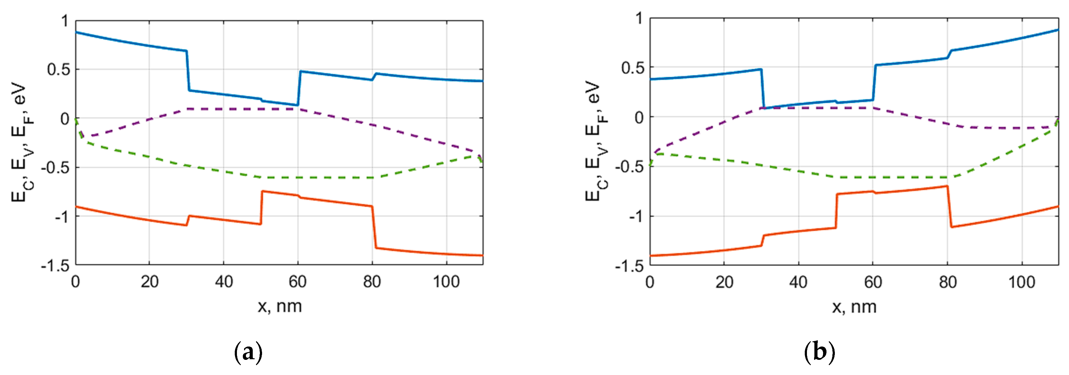
Figure 3 shows the energy band diagrams and spatial distributions of quasi-Fermi levels in the control heterostructure of the photodetector with controlled relocation of carrier density peaks (refer to the cross-section in
Figure 1). To obtain these and further results, we applied the combined numerical Model (1)–(8) with the boundary Conditions (9), (10) and the simulation technique proposed in
Section 4. The control heterostructure has the following configuration:
the 30-nm
n-type
region of the upper Schottky-barrier control junction (Position 1 in
Figure 1);
the 20-nm upper LT- layer (Position 2);
the 10-nm i-type absorbing region (Position 3);
the 20-nm lower LT- layer (Position 4);
the 30-nm n-type region of the lower Schottky-barrier control junction (instead of Positions 5 and 6).
Fractions
a,
b,
c,
d and
e for the components of A
IIIB
V semiconductor compounds were selected in order to provide the desired shapes of quantum wells. The concentration of ionized donors in both
n-type
regions is 10
17 cm
−3. The background impurity concentrations of 10
14 cm
−3 are specified in other layers. The height of both Schottky potential barriers at the control contacts is 0.8 eV. The initial control voltage that holds non-equilibrium charge carriers in the absorbing region equals to 0.5 V. The bias control voltage of reverse polarity that relocates carrier density maximums into the LT layers amounts to −0.5 V. At the initial time, the additional difference between electron and hole quasi-Fermi levels is induced in the absorbing region. It equals to 0.6 eV and is caused by the high densities of photogenerated charge carriers. Such difference corresponds to the input optical power of about 0.1 uW (according to Formula (14)) for the resonant cavity quantum efficiency of 0.87 (
, the reflection coefficients of mirrors are 0.45 and 0.95). In
Figure 3a, the initial control voltage is applied, and the carrier density maximums are located in the thin absorbing region.
Figure 3b corresponds to the completion of the relocation process, and the transverse transport of electrons and holes results in the spatial redistribution of electron and hole quasi-Fermi levels.
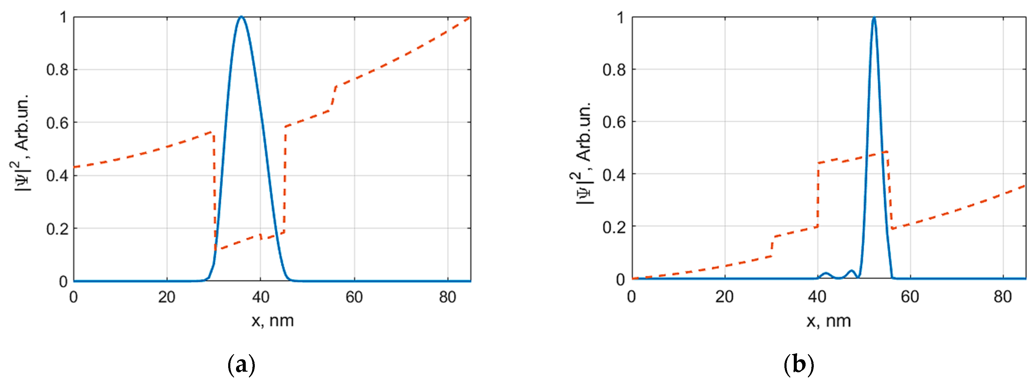
Figure 4 demonstrates the spatial distributions of probability densities (or the squares of wavefunction absolute values) for charge carrier location, in the regions of the control heterostructure.
Figure 4a is for electrons in the conduction band, and
Figure 4b is for holes in the valence band. Here, we consider another device configuration with the 10-nm upper LT-
layer (Position 2 in
Figure 1), the 5-nm
i-type
absorbing region (Position 3), and the 10-nm lower LT-
layer. The lengths of the Schottky-barrier control junctions are the same as in
Figure 3. Both panels of
Figure 4 correspond to certain energy levels of electrons and holes. We performed the curve calculations for the moment immediately after the end of the carrier relocation process, when the bias control voltage is still applied. Therefore, the maximums of electron and hole probability densities are displaced to the LT layers.
The spatial distributions of carrier densities in the control heterostructure of the photodetector with controlled relocation of carrier density peaks are given in
Figure 5. The device configuration is analogous to the one shown in
Figure 3. In the thin
i-type absorbing region (see Position 3 in
Figure 1), the maximums are overlapped (
Figure 5a). The LT layers (Positions 2 and 4) are the regions for the spatial separation of electron and hole density peaks under the influence of the control electric field (
Figure 5b).
Figure 5a corresponds to the instant just before the start of the laser pulse’s back edge (refer to the energy band diagram in
Figure 3a). In this case, control voltage equals to the initial value, and the transverse electric field holds photogenerated carriers in the thin
i-type absorbing region (see Position 3 in
Figure 1). Until the beginning of the back edge detection, the device operates as a standard
p-
i-
n photodiode. The strong longitudinal electric field in the active region separates photogenerated charge carriers and accelerates them along the
y axis to drift saturation velocity. Flowing through the supply circuit, non-equilibrium charge carriers induce a photocurrent.
Figure 5b demonstrates the distributions of electron and hole concentrations immediately after the end of the relocation transient process during the back edge of a laser pulse (refer to the energy band diagram in
Figure 3b). The transverse electric field of the control heterostructure separates the peaks of electron and hole densities and relocates them along the
x axis to the upper and lower LT layers (Positions 2 and 4 in
Figure 1), respectively. The total number of charge carriers in quantum wells remains nearly constant during the rapid relocation process. In the LT layers of the control heterostructure, carrier mobilities are lower, and lifetimes are significantly shorter than in the absorbing region (Position 3). The rapid change in carrier mobility and recombination rate leads to the faster relaxation of a photocurrent in the supply circuit, as compared to conventional
p-
i-
n photodiodes.
Figure 6 shows the results of the photocurrent calculation for two previously mentioned configurations of the photodetectors with controlled relocation of carrier density peaks. The reverse supply voltage of the photosensitive
p-
i-
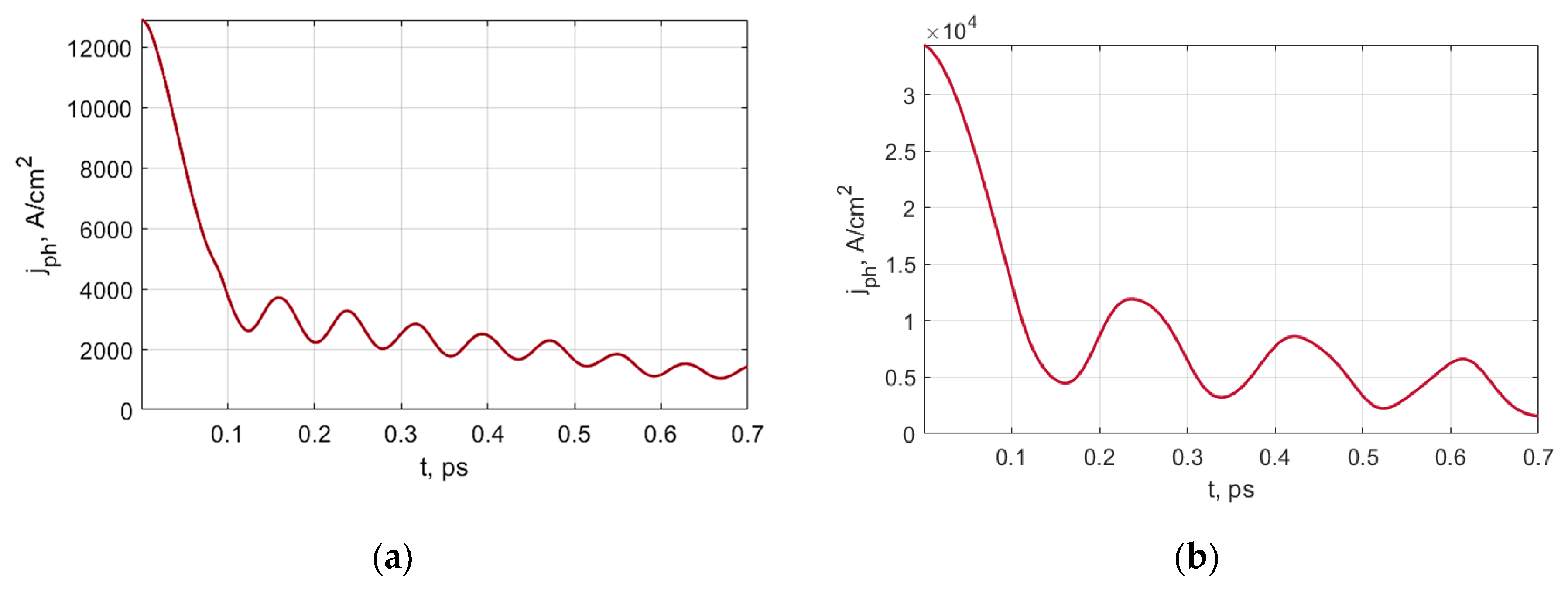
n structure is −0.5 V. We assume that electrons and holes in the LT layers have an identical lifetime of 0.4 ps. In other regions of the device, lifetime equals to 10 ps. Charge carrier mobilities in the LT layers are 75 times lower than in regular-temperature-grown regions. Within the time-domain simulation, we treat the idealized case: At
optical input instantly drop to zero and the control voltage instantly step to −0.5 V.
According to the curves given in
Figure 6, the back edge of the photocurrent pulse has two pieces. The first one has a steep slope and a duration of about 0.1 ps. It corresponds to the fast relocation of carriers from the absorbing region to the LT layers after the application of the bias control voltage. The second piece is gently sloping because of further recombination and transport processes in the LT layers. These processes are considerably slower than controlled relocation. The oscillations of current density are caused by the reflection of electron and hole wavefunctions from the heterointerfaces in the transverse direction, superposition of reflected waves and corresponding changes in carrier densities.
Figure 6 considers the detection of laser radiation with the input optical power of approximately 0.05 (panel a) and 0.1 uW (panel b). The power estimation was obtained using Formula (14) for a 1000-nm resonant cavity, mirror reflection coefficients of 0.45 and 0.95, and resulting quantum efficiency of 0.87. The length of the absorbing region along the
y axis is 200 nm.
6. Conclusions
Thus, we proposed the novel design of the high-speed photodetector for on-chip optical interconnections in ICs. The device employs the principle of controlled relocation of carrier density peaks within quantum wells of nanoheterostructure for the photocurrent back edge’s reduction to a subpicosecond value. The relocation is controlled by the transverse electric field of the control heterostructure. If zero or initial control voltage is applied, the maximums of electron and hole densities are overlapped in the thin absorbing region with high carrier mobilities and durable lifetimes. The bias control voltage separates the peaks and shifts them to the LT layers with low carrier mobilities and short lifetimes. Before the back edge start, the photodetector operates as a classical p-i-n photodiode, which provides the separation and transport of non-equilibrium charge carriers by the longitudinal electric field. Orthogonal orientations of the light direction, the p-i-n structure field and the control field, as well as for the response time improvement, allows for the maintenance of a high sensitivity.
To estimate the back edge performance of the photodetector with controlled relocation of carrier density peaks, we developed the combined time-domain numerical model that contains two components. The semiclassical equations describe longitudinal carrier transport and recombination, and the quantum-mechanical Schrodinger-Poisson equation system covers the transverse relocation process in quantum wells of the control heterostructure. For the implementation of the model, we proposed the scaling technique, the implicit discretization scheme, two computational algorithms, and applied software.
We obtained the numerical simulation results for the photodetector with controlled relocation of carrier density peaks. The duration of the steep part of the photocurrent back edge is about 0.1 ps, and it is determined by the rapid relocation process in the transverse direction.
At the next stage of the research, we will perform two-dimensional drift-diffusion simulation of the proposed device with due regard to carrier diffusion, high-field effects, and capacity recharge processes.


