Article

Electron Population Dynamics in Optically Pumped Asymmetric Coupled Ge/SiGe Quantum Wells: Experiment and Models

1
Department of Sciences, Università Roma Tre, Viale G. Marconi 446, I-00146 Rome, Italy
2
Department of Physics “Enrico Fermi”, Università di Pisa, Largo Pontecorvo 3, I-56127 Pisa, Italy
3
Department of Physics, Sapienza University of Rome, Piazzale Aldo Moro, I-00185 Rome, Italy
4
Institute of Ion Beam Physics and Materials Research “Helmoltz-Zentrum Dresden-Rossendorf”, D-01314 Dresden, Germany
5
Institut für Angewandte Physik, TU Dresden, D-01062 Dresden, Germany
6
IHP-Leibniz-Institut für innovative Mikroelektronik, Im Technologiepark 25, D-15236 Frankfurt (Oder), Germany
7
James Watt School of Engineering, University of Glasgow, Oakfield Avenue, Glasgow G12 8LT, UK
8
Institute for Quantum Electronics, Eidgenossische Technische Hochschule Zürich, 8092 Zürich, Switzerland
*
Authors to whom correspondence should be addressed.
Photonics 2020, 7(1), 2; https://doi.org/10.3390/photonics7010002
Submission received: 29 October 2019 / Revised: 13 December 2019 / Accepted: 16 December 2019 / Published: 18 December 2019

Abstract

:
n-type doped Ge quantum wells with SiGe barriers represent a promising heterostructure system for the development of radiation emitters in the terahertz range such as electrically pumped quantum cascade lasers and optically pumped quantum fountain lasers. The nonpolar lattice of Ge and SiGe provides electron–phonon scattering rates that are one order of magnitude lower than polar GaAs. We have developed a self-consistent numerical energy-balance model based on a rate equation approach which includes inelastic and elastic inter- and intra-subband scattering events and takes into account a realistic two-dimensional electron gas distribution in all the subband states of the Ge/SiGe quantum wells by considering subband-dependent electronic temperatures and chemical potentials. This full-subband model is compared here to the standard discrete-energy-level model, in which the material parameters are limited to few input values (scattering rates and radiative cross sections). To provide an experimental case study, we have epitaxially grown samples consisting of two asymmetric coupled quantum wells forming a three-level system, which we optically pump with a free electron laser. The benchmark quantity selected for model testing purposes is the saturation intensity at the 1→3 intersubband transition. The numerical quantum model prediction is in reasonable agreement with the experiments and therefore outperforms the discrete-energy-level analytical model, of which the prediction of the saturation intensity is off by a factor 3.

1. Introduction

Quantum cascade lasers (QCL) are based on intersubband transitions (ISBTs) among discrete energy states in quantum wells (QWs), and therefore, their operating principle is not limited to direct bandgap material systems [1]. The basic requirements that a semiconductor heterostructure hosting QWs has to comply with in order to be suitable for QCL development are a high quality of the heterostructure; a band offset compatible with the target emitted photon energy; and a small effective mass of carriers (holes or electrons). The small effective mass is beneficial both to obtaining a high laser gain and to avoiding extremely thin tunnelling barriers and confinement wells, which are difficult to grow due to unavoidable intermixing effects in alloy materials [2,3].
Electrons in n-type doped germanium (n-type Ge) have an effective mass m* = 0.13 me (me is the bare electron mass) that compares well with that of GaAs (m* = 0.067 me), thus fulfilling one main requirement for QCL designs. To achieve the required material quality, the lattice mismatch between Si and Ge requires strain-relaxed buffers of SiGe epitaxially grown on top of silicon substrates [4,5,6] and, for the active region, imposes the growth of strain-symmetrized Ge/SiGe heterostructures where tensile strained SiGe is used as the barrier material and compressive Ge QWs confine the electrons at the L-point minimum of the conduction band of Ge. The maximum band offset that can be obtained at the L-point with strain-symmetrised Ge/SiGe heterostructures with designs doable in practice for QCL is around 100 meV, limiting possible laser emission to photon energies in the terahertz (THz) range below about 30 meV. In the future, the use of ternary alloys SiGeSn may allow for higher band offsets at different points of the Brillouin zone [7,8]. In general, non-radiative lifetimes in Ge/SiGe QWs may be slightly longer than in equivalent designs realized in an AlGaAs/GaAs material system, due to the nonpolar nature of the Ge and SiGe lattices.
For accurate QCL designs, a numerical quantum model of electron state population dynamics out of equilibrium is required. Since an electrically pumped Ge/SiGe QCL has been designed but not realized yet [9,10,11], optically pumped devices may offer an easier experimental test bench to assess the performances of models with out-of-equilibrium intersubband (ISB) population dynamics. For optically pumped lasers, electrical contacts are not required, thus eliminating most of the device processing steps and related difficulties [12], and besides, much simpler active layer QW stacks are needed compared to QCLs. The basic structure for an optically pumped QW emitter consists of two asymmetric (i.e., of different thickness and/or composition) wells coupled through a thin tunnelling barrier (asymmetric coupled QWs, ACQWs) [13]. The QW that hosts the ground state (level 1) of the coupled structure is heavily doped, and the first two excited states (levels 2 and 3) are designed to operate as a three-level laser system, where levels 3 and 2 act as the upper and lower laser transition states, respectively. The working principle is the following: electrons are pumped to the upper transition level with a high-power optical beam tuned at the 1→3 ISBT, and then, radiative emission at the 3→2 ISBT is observed. Emission is ideally favoured by a fast, non-radiative depopulation of level 2, hence allowing population inversion between levels 2 and 3 which produces gain. Optically pumped lasers based on this three-level structure, called “quantum fountain lasers” (QFLs), have already been demonstrated in III-V compound heterostructures such as AlGaAs/GaAs, both in the mid-infrared (IR) and in the THz range [14,15]. However, the low radiative rates for THz emission from ISBTs implies that significant numbers of electrons have to be excited from level 1 to level 3 by the optical pump [16,17,18,19]. This translates into (1) the need for a high-power pulsed pump in the THz range, provided here by a free-electron-laser (FEL) [20,21]; (2) heavy n-doping of the ground state of the ACQWs; and (3) a high dipole moment of the 1→3 ISBT to enhance pump efficiency. These conditions, however, are detrimental for photon emission at the 3→2 transition, as they lead to (1) high electron temperatures under optical pumping; (2) high non-radiative scattering rates; and (3) scarce wavefunction overlap between levels 2 and 3, respectively. Therefore, lasing action under optical pumping in Ge/SiGe ACQWs has not been observed to date [22] despite absorption saturation being clearly observed.
The quality of both the heterostructure material and the numerical model for carrier dynamics can be then evaluated by comparison of experimental and simulation results of absorption saturation, as this phenomenon crucially depends on non-radiative lifetimes. Once the quality of the grown material and the reliability of the simulation platform have been assessed in the QFL model systems, these results can be translated in the design of the more complex QCL heterostructures. The heterostructure growth techniques used for QFLs are, indeed, precisely the same as those used for QCL structures [23,24]; the growth parameters are in the same range because the thickness of wells and barriers is precisely in the same range for both QFLs and QCL structures (few nanometers for barriers and 3 to 15 nm for wells). Interface roughness effects should then be identical, and so the electron scattering by interface roughness, which is known to be a major limiting factor for QCL operation. With these objectives in mind, we have designed and grown a series of ACQW samples made of n-type Ge/SiGe heterostructure material for THz absorption-saturation measurements and subsequent numerical model testing.

2. Materials and Methods

ACQW samples (potential profile sketched in Figure 1a) were grown epitaxially on low-impurity concentration Si (100) with the ultra-high-vacuum chemical vapor deposition (UHV-CVD) technique. To achieve SiGe layers at high Ge concentration with low threading dislocation densities (about 1 × 107 cm−2 on the surface), the active region of the samples has been deposited on top of a SiGe reverse-graded virtual substrate, where the lattice mismatch is gradually distributed among several layers [6]. The epitaxial layer structure of the active region is made of 20 periods of identical Ge/Si0.2Ge0.8 ACQWs in which a wide Ge well of width 12 nm is coupled to a narrow well that is 5 nm wide through a thin tunneling barrier having a thickness of 2.3 nm. The ACQW modules are separated by a 21-nm thick Si0.2Ge0.8 spacer. The detailed structural characterization of the samples shows the high quality of the heterostructures and reproducibility of deposited thickness in the subnanometer range [25]. The samples investigated here were n-doped by P co-deposition in the wide Ge well. The donor density has been calibrated by secondary ion mass spectrometry (SIMS) and the actual sheet-carrier density was directly measured by Fourier Transform Infrared (FTIR) spectroscopy, obtaining Ntot = 7 × 1011 cm−2 and 1 × 1011 cm−2 for samples S1 and S6, respectively. Samples were then cut and polished in a prism-waveguide geometry to couple the input radiation to the vertically polarized ISBT dipole (Figure 1b). The heterostructure design targeted comparable 1→2 and 1→3 oscillator strengths, obtained through strong hybridization of levels 2 and 3, respectively. Beyond increasing the optical pumping efficiency, this condition also enabled us to measure clear intersubband absorption signatures of both 1→2 and 1→3 ISBTs by absorption spectroscopy at equilibrium obtained by FTIR. FTIR transmission spectra were obtained in side-coupling configuration through the waveguide of Figure 1b with radiation polarized vertically (TM-polarized, parallel to the growth axis) and horizontally (TE-polarized, parallel to the QW plane). The ISBT absorption spectrum is obtained as A = −ln(TTM/TTE); TTM (TTE) is the transmittance measured with linearly polarized light. The samples were kept at cryogenic temperatures (T = 10 K) in an optical He-flow cryostat during the FTIR experiment.
Optical pumping of the 1→3 ISBT was experimentally achieved with quasi-monochromatic THz pulses from the FEL tuned at pump photon energies of ω p = 41.9 to 48.1 meV around E13 (338–387 cm1, 10.2–11.7 THz, or 25.8–29.6 μm) [22]. The pulse duration was Δtp ~ 10 ps with a Gaussian envelope, resulting in approximately 100 radiation cycles per pulse. The maximum peak power of Pin,max = 15 kW, calculated from a measured continuous-wave (CW) FEL power of 2.0 W and a duty cycle of 1.3 × 10⁴, results in a maximum peak pump intensity in vacuum Ip,max,vac = Pin,maxr2 = 1.9 × 10⁶ W/cm2, where r ~ 0.5 mm is the radius of the focal spot determined by inserting a THz camera at the sample position. We have determined that the pump intensity in the ACQW region is much lower than this vacuum value mainly because a copper screen with a rectangular slit aperture of 0.3 × 5.0 mm2, much smaller than the waveguide section of 0.5 × 8.0 mm2, was mounted before the sample in order to avoid any pump radiation to pass through the cryostat without passing through the waveguide. The combination of diffraction losses, electromagnetic mode mismatch at the waveguide input-facet and reflections at the cryostat windows lead to an estimated optical coupling efficiency factor ~ 6 × 10³. This is mostly due to the edge coupling of terahertz radiation into the sample (thickness 0.5 mm) with a mismatched focal spot diameter of 8.0 mm (FTIR) or 1.0 mm (FEL). Furthermore, we used a rectangular aperture of 0.3 × 5.0 mm2 in front of the sample edge to eliminate stray light. To estimate , we have measured the absolute transmittance at 30-μm wavelength by FTIR, using the intensity measured with a focal spot diameter of 8.0 mm or 1.0 mm as reference for the intensity transmitted by the slit-sample mounting in FTIR or FEL experiments. In the FTIR experiment, the absolute transmittance was 0.1%. In the FEL experiment, the transmittance is estimated to be around 0.9%. A further factor 0.7 comes from cryostat window reflections. The saturation of absorption due to the pump action in the three-level ACQW system was measured by increasing the FEL pump beam intensity from almost zero to the maximum available power using metal mesh attenuators. The samples were mounted in the sample holder so as to have the FEL radiation in TM polarization inside the slab waveguide. Simultaneously, the incident and the transmitted radiation intensities, Din and Dout, were measured with calibrated pyroelectric detectors (see Figure 2d for a scheme of the optical setup). Similar to the FTIR experiment, the samples were kept at cryogenic temperatures (TL = 6 K) in an optical He-flow cryostat. More experimental details can be found in References [22,25].
Numerical simulations are performed using a self-consistent energy-balance model based on a rate equation approach for intersubband carrier relaxation dynamics after pulsed optical excitation. The dynamics of subband populations and energies is calculated from their equilibrium values (obtained through a multivalley effective mass Schrödinger–Poisson solver) by solving coupled differential equations describing the time derivatives of energy and populations in terms of inter- and intra-subband scattering events, including inelastic (optical phonon) and elastic (ionized-impurity, interface roughness) channels. The model features subband-dependent electronic temperatures and chemical potentials, thus taking into account the actual two-dimensional electron gas (2DEG) distribution in the subbands and, consequently, for example, thermal activation of phonon-mediated intersubband transitions [26].

3. Results

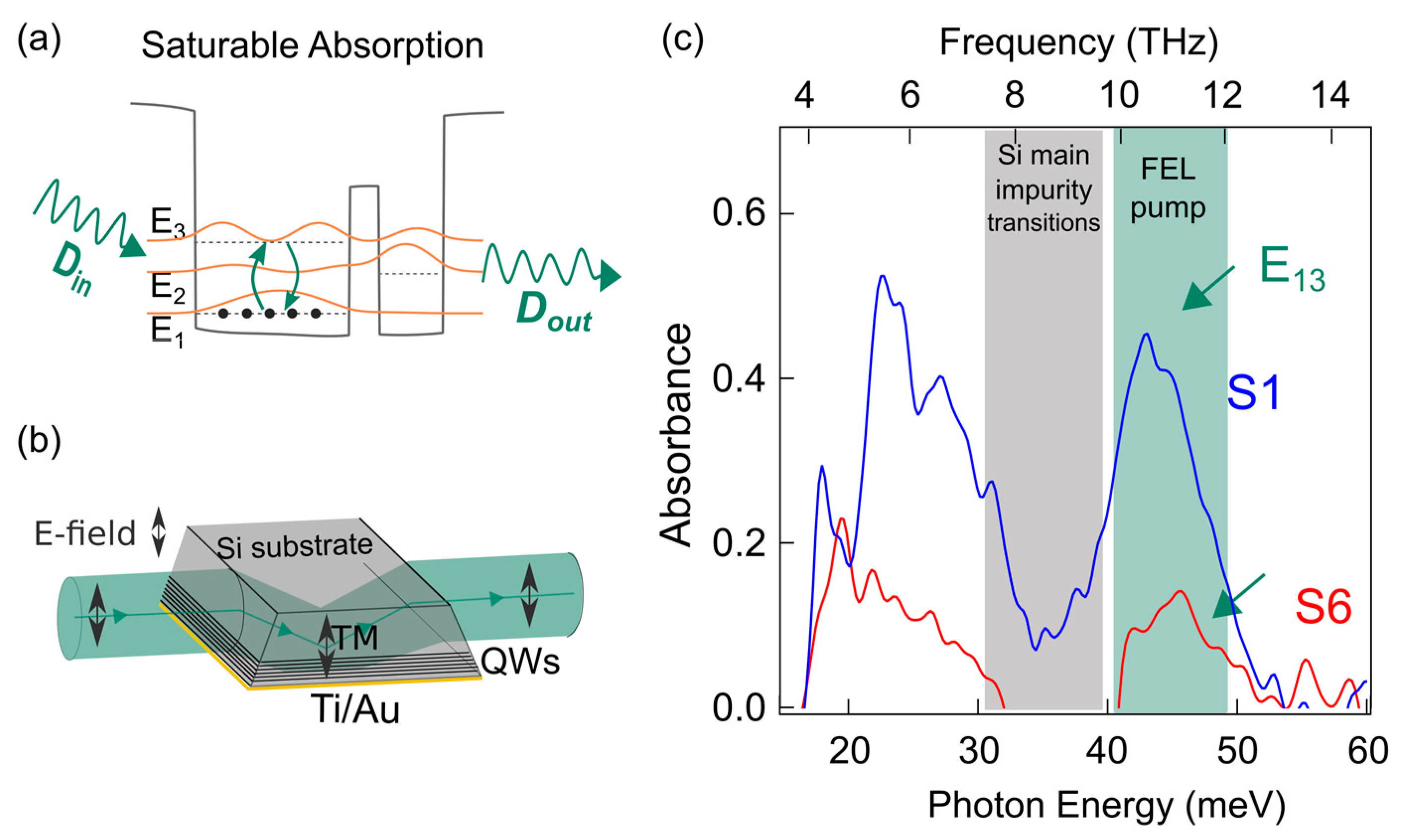
3.1. Spectroscopy at Equilibrium

The absorption spectra measured by FTIR are shown in Figure 1c and display two peaks centered at the photon energies E12 and E13 in both samples S1 and S6, with an intensity ratio between S1 and S6 approximately matching the doping level ratio of 7 between the two samples. In both samples, the two peaks have similar intensity, indicating strong hybridization between the states of the two coupled wells, as from design targets. The ISBT absorption energies and intensities correspond well to the values calculated with a Poisson–Schrödinger solver after the depolarization shift has been taken into account [25]. We then define the surface-normal ISBT dipole strength zij from the following bra-ket:
z ij = | ψ j | z | ψ i | 2
where ψi is the envelope wavefunction of the i-th subband. For both sample S1 and S6, we obtain z12 ~ 3 nm, z23 ~ 5 nm, and z13 ~ 2 nm. In terms of the oscillator strengths fij =|zij|2 2 m ω ij / , with ωij = E ij t h e o / , we achieved f13 = 0.7 f12 for sample S1 (f13 ~ 0.4 and f12 ~ 0.6) and f13 = 0.8 f12 for sample S6 (f13 ~ 0.45 and f12 ~ 0.55). The precise determination of the transition energy E13 from the absorption spectra of Figure 1c has allowed us to precisely tune the optical pump photon energy at the 1→3 ISBT maximum at 10.5 THz or to slightly detune it if required (green shaded area in Figure 1c), hence exploiting the full tunability of the FEL. Notice that the range between 8 and 9.5 THz has been carefully avoided both in the design and in the pump experiment because of the presence of absorption lines due to transitions between impurity states in the silicon wafer substrate, which would interfere with the ISBTs.

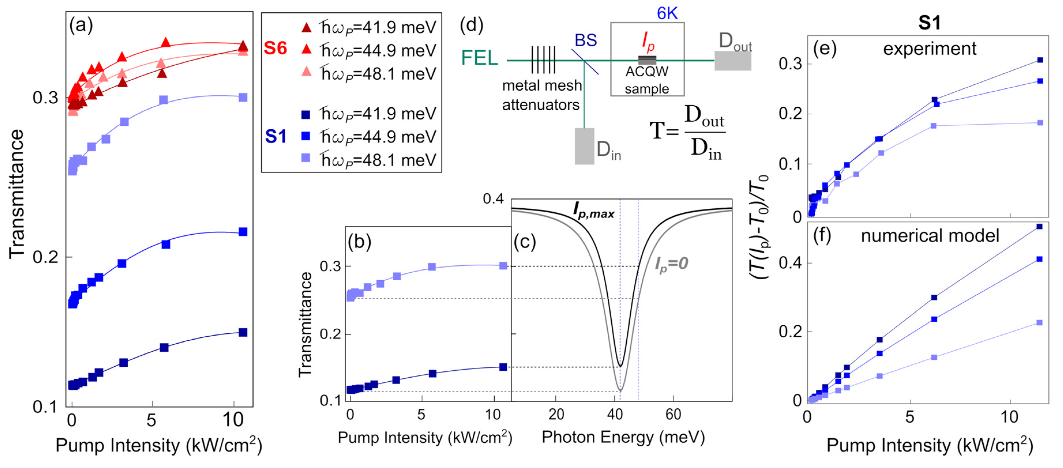
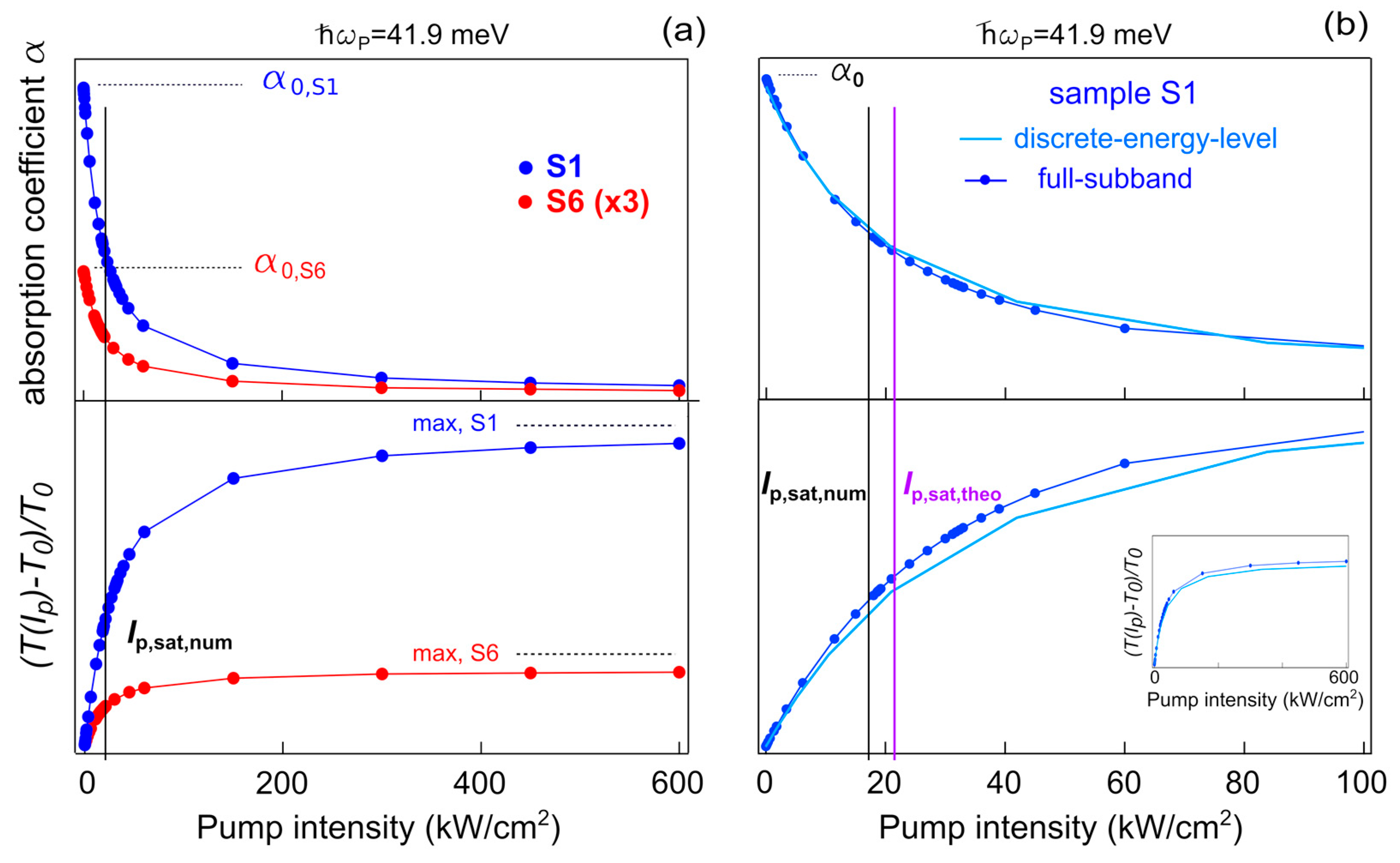
3.2. Absorption-Saturation Experiment

The actual pump intensity in the ACQW region, as discussed in the methods section, is Ip,max = Pin,maxr2 = 11 kW/cm2. For comparison, the pump intensity obtainable with a THz QCL with peak power of less than 1 W is three to four orders of magnitude lower than Ip,max obtained here with the FEL. In Figure 2a,b, the T(Ip) plots show the transmittance as a function of the pump intensity for S1 and S6 at the three pump photon energies explored. The zero-intensity transmittance value T0 = T(Ip→0) is calibrated with a Lorentz oscillator model of the transmittance based on FTIR data for each sample, temperature, and pump photon energy (Figure 2c). A nonlinear increase of T(Ip) is clearly observed in Figure 2a at all the investigated pump photon energies for both samples. In particular, the lightly doped sample S6 demonstrates a transmission increase of 10% at Ip,max at all ω p , whilst the heavily doped sample reaches an increase of transmission above 25% for resonant pumping at ω p = 41.9 meV. This is consistent with the effectiveness of heavy doping in increasing the amount of saturable ISBT losses with respect to non-saturable optical transmission losses. In Figure 2e, we report the relative transmittance change (T(Ip) − T0)/T0 for sample S1 for all the pump photon energies employed; this quantity can be directly compared with the results of the numerical simulations (Figure 2f) based on the full-subband model described in the following section.
We now discuss how to obtain an experimental value for the saturation intensity Ip,sat,exp from the analysis of the absorption-saturation data in Figure 2. A proper fitting function to our samples should take into account the finite length of the sample and the non-saturable loss mechanisms; therefore, the widely employed simplified fitting formulas for saturable absorption [27,28,29], valid only for ultrathin film absorbers, cannot be used here. For this reason, we employ the optical model for the intensity-dependent transmittance of a finite-length saturable absorber proposed in Reference [30] and recently used in Reference [31]. The fitting equation, reported as continuous curves in Figure 2a,b, is as follows:
T ( I p ) = T ns ln ( 1 + T lin / T ns ( e I p / I p , sat 1 ) ) I p / I p , sat · e I p I p , abs
where Tlin represents the linear (i.e., vanishing intensity) transmittance, which we identify with T0 estimated from FTIR. The non-saturable losses are taken into account through the parameter Tns, obtained from the FTIR spectra analysis of an undoped reference. This term represents the fact that, even in the absence of ISBT absorption, the transmittance does not reach unity due to reflection losses and absorption in the substrate. Tlin and Tns then contain the dependence on the photon energy and on the sample length. The maximum theoretical level of saturable losses for a given sample and pump photon energy is given by the difference (TnsTlin), which is higher for heavier doping and/or for pump photon energy closer to the ISBT resonance because the value of Tlin is lower, while Tns is instead set to around 0.4 by optical transmission losses independent of doping (see Figure 2c). The exponential term depending on Ip,abs accounts for the pump-induced increase of the absorption [30], mainly attributed to the weak interaction of the FEL pump beam with shallow impurities in the silicon wafer. The interaction is weak because the pump photon energy is far from the impurity photoionization lines at 25–39 meV (see grey shaded area in Figure 1c); however, the 0.5-mm thick wafer substrate has a 103 times larger interaction volume with the pump beam than the 400-nm thick ACQWs region. The interaction of the FEL pump with our low-impurity-density silicon wafer can be summarized as a weak bleaching of transitions between bound impurity states for low and intermediate intensities and dominant pump-induced absorption for high intensities [32,33,34]. The exponential factor at the end of Equation (9) phenomenologically reproduces this behaviour.
The saturation intensity depends only on intrinsic quantum-mechanical quantities obtained by wavefunction integrals, such as the transition dipole moments and the non-radiative lifetimes; see Equation (10) below, which are almost identical in all our samples. Therefore, a global fitting of Equation (2) to the all data of Figure 2 was performed, and it provided a value for Ip,sat,exp = 7.2 kW/cm2, within a 30% range of allowed variation among the two doping levels and the three pump photon energies.

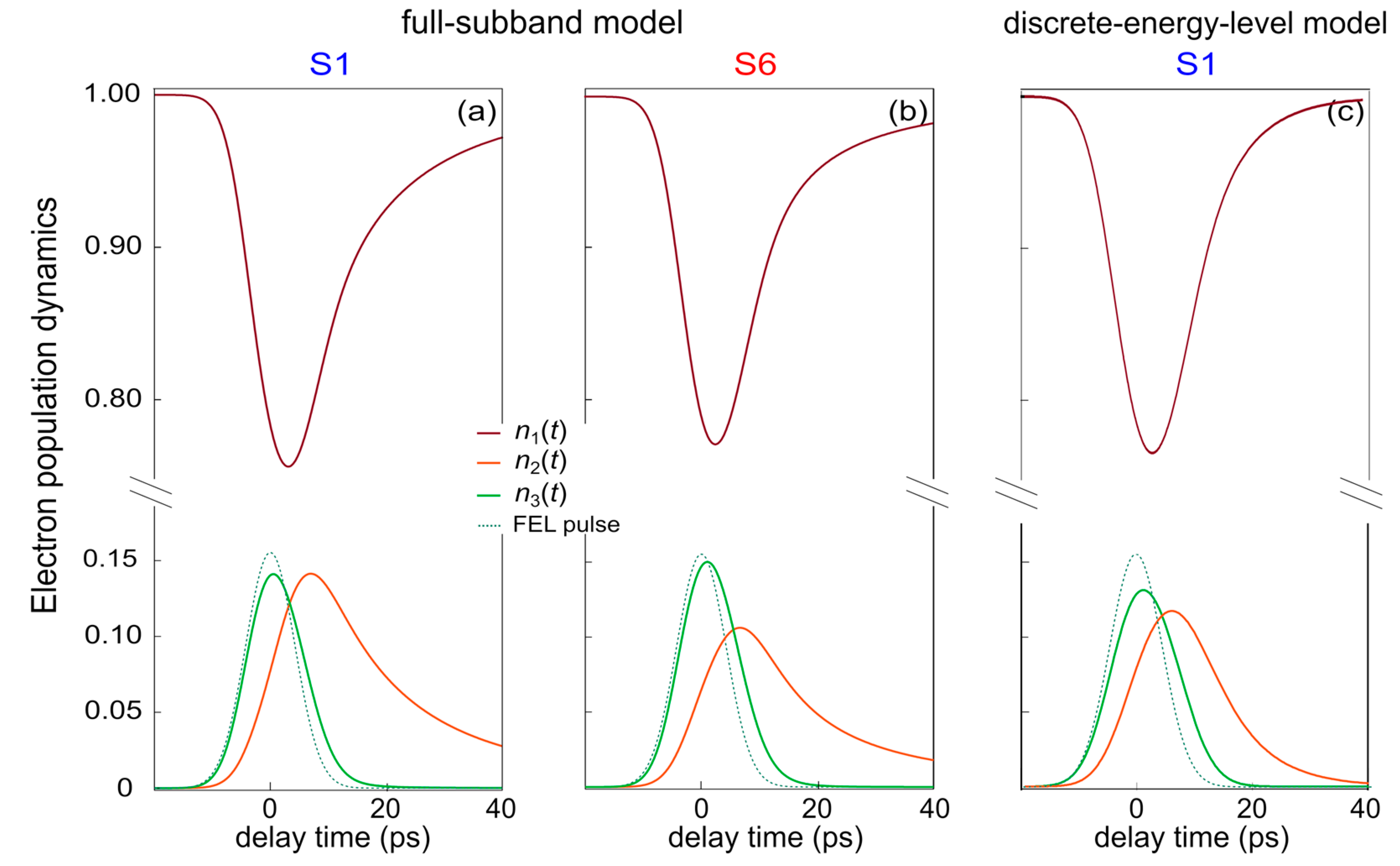
3.3. Numerical Simulations of Subband Population Dynamics

A very important fact for the present study is that the non-radiative relaxation lifetimes of excited states in Ge/SiGe are predicted to be longer than in III-V compounds and less dependent on temperature. In fact, in nonpolar group-IV semiconductors the electron–phonon interaction is controlled by the deformation-potential interaction, which is much weaker than the Frӧhlich interaction featured by the polar lattices of III-V compounds [35]. This effect can be quantified by analyzing Figure 3. We consider a generic rectangular QW and evaluate the net transition rate for the 2→1 transition due to absorption or emission of phonons Wnet21 = < W21 > − < W12 >, where the symbol < > indicates the statistical average over all possible electron distributions at a given electron gas temperature Te. The phonons involved in the non-radiative relaxation are mostly longitudinal optical (LO) phonons with very long wavelength. Figure 3a shows Wnet21 between the first excited subband and the fundamental subband of a generic QW, as a function of the energy separation E21. The rate has been calculated for ideal semiconductors with a polar and a nonpolar lattice (blue and red curves, respectively), featuring a single LO phonon at 37 meV to be considered as an oversimplified model of GaAs and Ge. The dipole-active optical phonon of the polar lattice generates a kind of resonance around 37 meV in Wnet21, which then decreases at higher E21. The nonpolar phonon instead produces only a step-like feature because no resonant dipole interaction is possible between the phonon and the ISBT at energy E 12 = ω LO . More precisely, in nonpolar semiconductors. the coupling term for the electron–phonon interaction does not depend on the exchanged momentum; then, Wnet21 resembles a step-like function because only energy conservation is relevant in each electron–phonon scattering event. On the other hand, in polar materials, the coupling term is inversely proportional to the exchanged momentum, which is zero only when E 12 = ω LO   because the initial and final electronic states have the same crystal momentum (non-radiative vertical transition). Note that the red curve has been multiplied by a factor 10, indicating that Wnet21 is much smaller in nonpolar than in polar lattices at all energy separations due to the lower strength of the deformation potential interaction if compared to that of the Fröhlich interaction.
In Figure 3b, the calculation of Wnet21 is repeated considering the actual 2DEG distribution of electrons in the subbands corresponding to a sheet carrier density n2D = 1 × 1011 cm−2, a typical level employed in the optical pumping experiments. Following Reference [36], we properly take into account the Pauli blocking effect; moreover, the statistical average, performed over the electronic distribution relying on the expressions derived in Reference [37], allows us to include in the calculation the effects due to in-plane kinetic energy dispersion of the electrons in the two subbands or, in other words, of the excess electronic effective temperature. This fact is of key relevance to evaluate the correct relaxation time, especially when the subband separation is close to or below the optical phonon energy. Indeed, also for QWs with E21 below the phonon energy threshold at 37 meV, the emission of optical phonons can be activated by the high kinetic energy of the electrons in the upper subband (high subband excess electron temperature) and, thus, relaxation times can be largely overestimated if the single-particle empty-subband approximation is made [38], as often done in the literature [7,39,40,41].
In the following, the ISB non-radiative lifetimes have been calculated from a full-subband population dynamics model [42] based on equations similar to those that lead to the results of Figure 3 but are adapted to the specific ACQW samples and consider the optical pumping conditions of the present work. In particular, to correctly account for inter- and intra-subband particle and energy fluxes in ACQWs, we included here, in addition to electron–phonon scattering, the contribution of the elastic scattering channels due to interface roughness (assuming an interface roughness amplitude of 0.2 nm with correlation length of 7.0 nm [12]) and to ionized impurity. In fact, the latter is expected to play a role at the high doping levels required for QFLs. On the other hand, the impact of the interface roughness channel is much more pronounced in ACQWs samples with respect to single QWs because of the presence of a larger number of heterointerfaces in ACQWs and the larger amplitude of the electron wavefunctions at the heterointerface position due to the strong electron delocalization between the two coupled wells.
In Figure 4, we plot the population dynamics under optical pumping using the same experimental value of Ip,max = 11 kW/cm2 as the pump intensity. Numerical results obtained with the full-subband model, reported in Figure 4a,b for samples S1 and S6 respectively, are compared to the results obtained for sample S1 with the discrete-energy-level analytical model (Figure 4c), described in the following section. While in the latter model the actual kinetic-energy distribution of electrons in the subband is completely neglected, in the full-subband numerical model the relaxation dynamics at each time step depends not only on the subband populations but also on the specific subband electron energy distribution. We now see how this impacts the relaxation dynamics. We note that, for both the models, the population dynamics of the upper state n3(t) = N3(t)/Ntot closely tracks the time profile of the pump pulse (the dotted lines in Figure 4). A peak value n3,max ranging between 0.12 and 0.15 is obtained in all our samples. The fast decay of n3(t), which hampers population inversion, is due to the fact that E31 is practically equal to the relevant LO phonon energy (37 meV); therefore, the 3→1 non-radiative transition assisted by LO phonon emission is highly probable at any temperature. At short delay times, the dynamics of n2(t) is dominated by fast elastic scattering of electrons from subband 3, which determines the initial rise of n2(t) and hampers population inversion between level 3 and 2, which is achieved only during the first half of the pump pulse. The high initial potential energy of electrons in subband 3 is converted in a high kinetic energy when they are elastically scattered in subband 2. In the full-subband model, from the resulting high average kinetic energy for electrons in subband 2, we estimate an excess Te > 100 K, a value significantly higher than TL = 6 K. The high Te achieved allows to activate fast inelastic phonon-mediated scattering events involving hot electrons in subband 2, which transfer to subband 1. It then follows a rapid drop of Te in subband 2. The cooling of subband 2 coincides with the slower decay of n2(t) observed at longer delay time, since inelastic scattering events 2→1 become energetically forbidden. This drop in the depopulation rate of subband 2 is therefore intimately related to the dynamic modifications of the 2DEG distribution in subband 2, and it can only be predicted by the full-subband model.
We now discuss how, from the full-subband numerical model, we can estimate the relative transmittance change (T(Ip) − T0)/T0, to be compared to the experimental counterpart. We first evaluate the absorption coefficient α13(Ip) = σ13 (N1N3) at several pump intensities for both samples at the photon energy of 41.9 meV (upper panel of Figure 5a). Considering the temporal evolution of the populations N1 and N3, α13(Ip) varies over delay times. Here, α13(Ip) has been determined as the value corresponding to the minimum population difference N1N3 typically achieved at times close to t = 0 for a given pulse intensity level. The quantity T(Ip) has been obtained from the absorption coefficient through the relation T ( I p ) = e α ( I p ) L , with the optical path length in the QWs, L, depending on the internal reflection angle, the number of repetitions of the ACQW structure. and the waveguide length. From T(Ip), we calculate the relative transmittance change (T(Ip) − T0)/T0 with respect to T0 which is the transmittance at zero pump intensity measured by FTIR. The results are shown in the bottom panel of Figure 5a for both the samples S1 (blue curve) and S6 (red curve). The same quantity simulated for S1 for all the pump photon energies employed in the experiment is reported in Figure 2f. From the (T(Ip) − T0)/T0 curve of sample S1, we obtained a numerical estimate for the saturation intensity Ip,sat,num = 17 kW/cm2 as the pump intensity at which the transmittance change reaches a factor 1/e of its saturated value (black line mark in Figure 5a). For sample S6, the same procedure gives Ip,sat,num = 15 kW/cm2, which coincides with the estimate for S1 within uncertainties due to numerical sampling of the intensity. Therefore, the saturation intensity, is found to be sample-independent (Table 1).

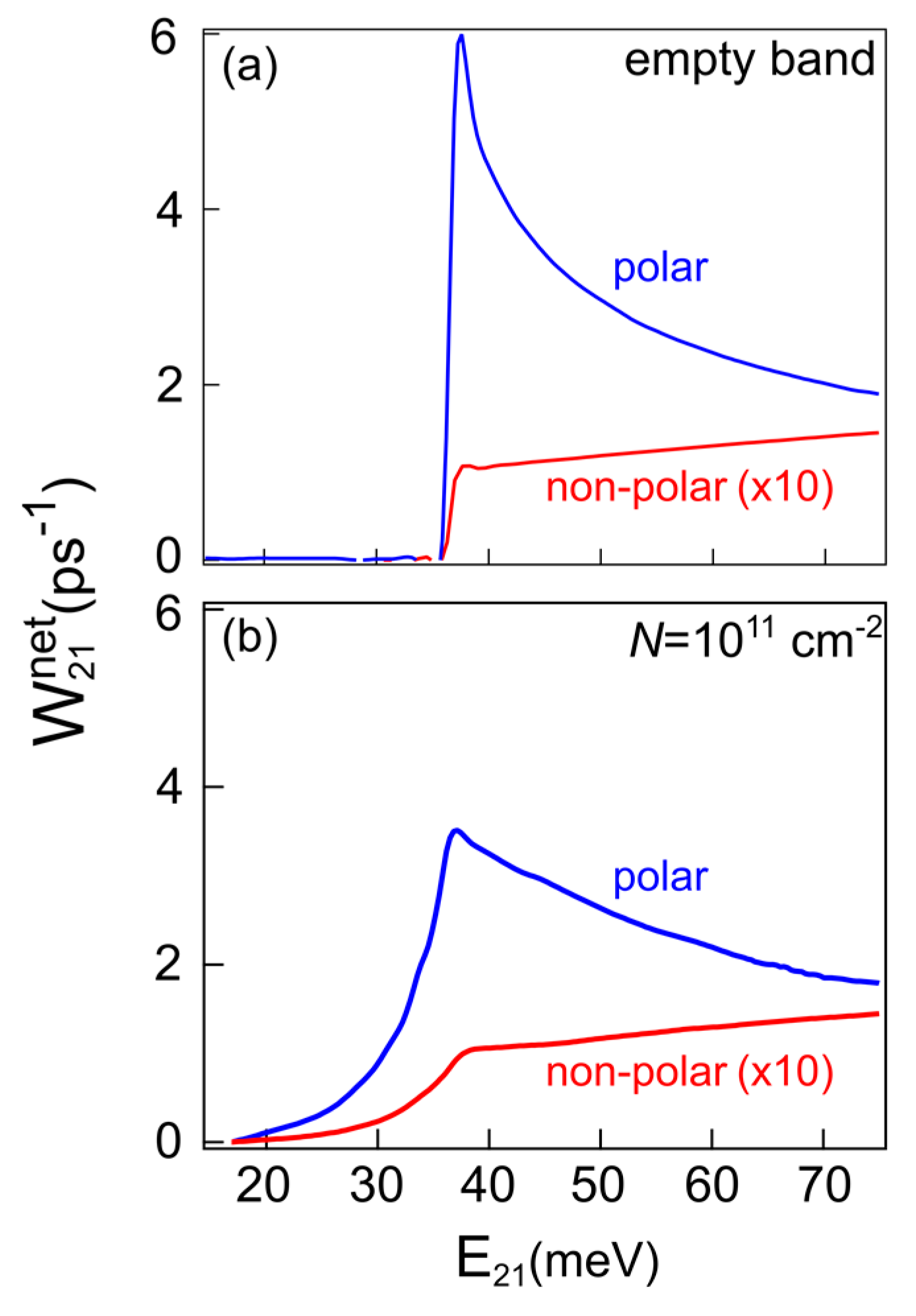
3.4. Analytic Solution of the Discrete-Energy-Level Model

We now solve the standard rate equation system associated with optical pumping of ACQWs in the three-discrete-energy-level model. From the analytic solution of the rate equation system, one can derive an explicit theoretical expression for the saturation intensity, Ip,sat,theo, which is instructive but valid only in the steady-state approximation (continuous wave optical pumping). Therefore, to directly compare the three-discrete-energy-level model with the results of the full-subband numerical model, we also solve the rate equation system in an implicit form corresponding to pulsed optical pumping. In the discrete-energy-level approximation, each level is formed by N-times degenerate states belonging to a subband, while the energy distance between levels Eij and the transition rates τij do not depend on the specific position in the subband. Each level can be filled with a time-dependent fraction of the total electrons ni(t) = Ni(t)/Ntot, which can scatter among the subbands vertically but not within the states of the same subband. The complete system of rate equations for the subband population can be written as follows [43]:
d n 1 d t = w ( n 1 n 3 ) + n 2 τ 21 + n 3 τ 31 n 1 τ 12 n 1 τ 13 d n 2 d t = n 3 τ 32 n 2 τ 21 + n 1 τ 12 n 2 τ 23 d n 3 d t = w ( n 1 n 3 ) n 3 ( 1 τ 32 + 1 τ 31 ) + n 1 τ 13 + n 2 τ 23
where τij are inverse non-radiative scattering rates (assuming the spontaneous radiative emission rates as negligible) and ω is the stimulated absorption/emission rate related to the optically pumped radiative transition 1→3 (see sketch in Figure 1a), given by the following:
w = σ 13 T 2 ω p   I p c o s θ
where T2 ≈ 0.15 ps is the coherence time of the electron states forming level 3 [44,45], which is a measure of the inverse homogeneous ISBT linewidth [42], and σ13 is the absorption/emission cross section per unit bandwidth calculated from the following formula [46]:
σ i j = π e 2 ε 0 ε r c ω i j | z i j | 2
where e is the elementary charge, c is the speed of light in vacuum, ε0 is the dielectric constant of vacuum, and √εr = 4.0 is the square root of the relative dielectric constant. From this formula, we calculate σ13 ∼ 0.13 cm2s−1 at ω p   = 41.9 meV, but a similar value is obtained for all the photon energies used for the experiment considering the small detuning among them. For the maximum intensity available in the experiment, Ip = Ip,max = 11 kW/cm2 and considering a propagation angle of the light in the waveguide of θ = 75°, we can now calculate w ∼ 1.3 × 10¹¹ s−1.
The non-radiative lifetimes τij used as inputs for the discrete-energy-level model have been estimated with the full-subband model but adopt the empty band approximation. In this approximation, we artificially set for each subband a very low electron temperature and Fermi energy close to the bottom of the subband to guarantee that the dynamics do not suffer from Pauli blocking. For sample S1, we obtain τ32 = 5.9 ps, τ21 = 7.3 ps, and τ31 = 2.2 ps, and for sample S6, we obtain τ32 = 7.1 ps, τ21 = 8.5 ps, and τ31 = 2.1 ps.
The upward non-radiative processes 1→2, 1→3, and 2→3 in general are much less probable than the respective downward processes at low temperature due to negligible thermal phonon population at TL = 6 K. This would not be the case at room temperature, where upward non-radiative processes may become relevant. For the present discussion, we can simplify the system of equations in Equation (3) to the more commonly used equations of the three-level laser system [23,44]:
d n 1 d t = w ( n 1 n 3 ) + n 2 τ 21 + n 3 τ 31 d n 2 d t = n 3 τ 32 n 2 τ 21 d n 3 d t = w ( n 1 n 3 ) n 3 ( 1 τ 32 + 1 τ 31 )
This system has been solved numerically using Ip(t) with Gaussian shape corresponding to the FEL pulses shown as dotted curve in Figure 4. The resulting ni(t) solutions are shown in Figure 4c. Since the 3→1 transition mediated by optical phonon emission is energetically allowed also at the minimum of subband 3, the dynamics of n3(t) do not strongly depend on the electron energy distribution in subband 3 and, therefore, both the full-subband and the discrete-energy-level models give similar results. A completely different behavior is observed for n2(t). The multiscale dynamics of subband 2 (i.e., the change in its depopulation rate over time), which is related to the dynamic modification of the 2DEG distribution in subband 2 is well described by the full-subband model and is not present in the discrete-energy-level model, since the relaxation times are fixed and estimated in the empty-band approximation. Accordingly, Pauli-blocking effects are also not included and we observe that the discrete energy model underestimates n2(t) at long delay times. The same quantities of Figure 5a can be modeled using the discrete-energy-level analytical model paying, as already stated above, the price of neglecting the energy distribution of electrons in the three subbands. The solution of the rate equation system in Equation (6), giving rise to the population dynamics of Figure 4c, has been obtained using the values of τij reported above, which were obtained from the same electron scattering model used to calculate the electron population dynamics in subbands. From N1N3, we calculated the absorption coefficient and the relative transmittance change following the same procedure described in the previous section. The results of these calculations are shown in Figure 5b for sample S1. A value of Ip,sat,theo ∼ 21 kW/cm2 can be found for the heavily doped sample S1 as the pump intensity at which the transmittance change reaches 1/e times its maximum value as done for the full-subband model (violet curve in Figure 5b). For comparison, Ip,sat,theo ∼ 23 kW/cm2 is the value found for sample S6 (not shown).
If instead we make the steady-state approximation (i.e., dni/dt = 0), it may be shown by simple algebra that, using the sum rule n1 + n2 + n3 = 1, the electron populations of the three levels described by Equation (6), are as follows:
n 1 = w + 1 τ 31 + 1 τ 32 w ( 2 + τ 21 τ 32 ) + 1 τ 32 + 1 τ 31 n 2 = w τ 21 τ 32 w ( 2 + τ 21 τ 32 ) + 1 τ 32 + 1 τ 31   n 3 = w w ( 2 + τ 21 τ 32 ) + 1 τ 32 + 1 τ 31
As stated above, at Ip,sat, the transmittance change is 1/e times its maximum increase and this roughly corresponds to a “saturated” absorption coefficient decreased to the half of its zero-intensity value. This latter definition can be expressed through the commonly employed general formula:
α ( I p ) α 0 1 + I p / I p , sat  
with α(Ip) = σ13(N1N3) = σ13(n1n3)Ntot and α0 = σ13Ntot.
The cross section σ13 and the total number of electrons Ntot appear both at the numerator and denominator of Equation (6); therefore, the explicit analytical expression for Ip,sat,theo can be obtained simply from the relative population difference (n1-n3) calculated in Equation (7).
n 1 n 3 = 1 τ 31 + 1 τ 32 w ( 2 + τ 21 τ 32 ) + 1 τ 32 + 1 τ 31 = 1 1 + [ w ( 2 + τ 21 τ 32 ) 1 τ 32 + 1 τ 31 ]
From the difference (n1-n3) written as a function of the pump intensity and using the definition of w in Equation (4), one can finally calculate the explicit analytical expression for the saturation intensity in the three-level system, optically pumped at the 1→3 transition:
I p , sat , steady = ω p c o s θ σ 13 T 2 ( τ 31 + τ 32 2 τ 32 τ 31 + τ 31 τ 21   )
giving as a result Ip,sat,steady = 17 kW/cm2 and Ip,sat,steady = 19 kW/cm2 for samples S1 and S6, respectively. Even though these values are in agreement with the results estimated from the two time-dependent models, we remark that the expression in Equation (10) is strictly valid only in the steady-state approximation. However, its explicit analytical form demonstrates a number of instructive features of the three-level saturation intensity: it does not depend on the pump photon energy ω p , as it cancels out in σ13; it weakly depends on the temperature and the detailed sample structure, since σ13 and τij are weakly temperature dependent; the dependence on the doping level is entirely due to the impurity scattering rates, which only partly impact on the total scattering rates.

4. Discussion

The sample characterization presented in Section 3.1 demonstrates the feasibility of the growth of high-quality quantum-well Ge/SiGe heterostructures by UHV-CVD. The FTIR absorption spectroscopy data of Figure 1c are in good agreement with the theoretical prediction based on the heterostructure parameters as determined by transmission electron microscopy, which are by themselves in agreement with the design values [25]. This fact calls for efforts towards the development of Ge/SiGe quantum well emitters both optically pumped (quantum fountain lasers) and electrically pumped (quantum cascade lasers).
We have introduced the saturation intensity Ip,sat as a benchmark quantity among the analytical discrete-energy-level model, the numerical full-subband model, and the experiments. The results are summarized in Table 1. Ip,sat,theo are obtained from the solution of the rate equation model shown of Figure 4c. Ip,sat,exp is imposed to be the same for the two samples by our global fitting procedure in Figure 2; therefore, values and error bars are identical in Table 1, and the error bar is intended as the maximum-to-minimum variation of the parameter value in the different fitting procedures to all datasets in Figure 2. Ip,sat,num is determined from Figure 5a, and it turns out to be sample independent within errors. The uncertainty of Ip,sat,num is related to the error propagation of the lifetimes. The discrepancy between the experimental and the numerical estimate of the saturation intensity is a factor 2 only. We consider this discrepancy to be small because, in the experiment, many other effects contribute to the intensity dependence of the transmittance, e.g., pump-induced absorption from impurities in the silicon wafer [22]. Conversely, the values of Ip,sat,theo in Table 1 depart from the experimental Ip,sat,exp by a factor of 3, indicating that the full-subband model outperforms the discrete-energy-level model. The full-subband model is much more performant since it takes into account the subband kinetic energy dispersions, giving therefore a better description of the actual scattering mechanisms, including thermally activated phonon emission and backscattering events from a lower to an upper subband. Since the discrete-energy-level model does not consider high electron temperature effects, it is not possible to model correctly the effect on the dynamics of the electronic temperatures in the subbands, which are particularly high in the nonpolar Ge/SiGe systems with respect to III-V materials as a direct consequence of the reduced electron–phonon coupling [11]. The specificity of Ge/SiGe is, thus, almost lost in the discrete-energy-level model. Nonetheless, the discrepancy between the two models (Ip,sat,theo being 20% higher than Ip,sat,num) indicates that the standard three-level analytical model can be used as a first rough approximation in the calculation of the pump intensity needed in an optically pumped experiment as long as well-estimated non-radiative lifetimes and the cross section are inserted as external input parameters.
In perspective, THz photoluminescence (PL) emission spectroscopy from Ge/SiGe ACQWs could be also used as an analysis tool for the material quality of samples with designs resembling those of QCL. To this aim, we now use the wavefunctions obtained from the solutions of the Poisson–Schrödinger solver to evaluate the spontaneous emission efficiency in Ge/SiGe ACQWs. The absorption spectra estimated from these wavefunctions reproduce the FTIR absorption spectroscopy data, as described in Reference [25]. Considering that the transition dipole is almost parallel to the growth direction z, the spontaneous radiative lifetimes are evaluated according to the following relation [18,46]:
τ rad , ij 1 = 2 3 e 2 ω ij 3 ε r 4 π ε 0 c 3   | ψ j | z | ψ i | 2
where the symbols are defined in Equations (1) and (5). For sample S1, this gives τrad,32 ~ 20 μs for the 3→2 transition and τrad,21 ~ 10 μs for the 2→1 transition. Fitting the calculated temporal evolution of the subband populations n2(t) and n3(t) with an exponential decay function starting after the excitation pulse peak, we obtain for the lower subband lifetime τrelax,2 ~ 17 ps for S1 and 15 ps for S6 and for the upper subband lifetime τrelax,3 ~ 3 ps for S1 and 6 ps for S6. Regardless of the numerical prefactors determined by slight differences in the ACQW design, we then obtain a quantum efficiency ηGe (approximated to the non-radiative/radiative lifetime ratio) for the 3→2 transition of ηGe ~ τrelax,3/τrad,32 ~ 3 × 10⁻⁷. For a hypothetical device targeting 2→1 emission, we would get a slightly higher ηGe ~ τrelax,2/τrad,21 ~ 15 × 10−7; however, this scheme is more difficult to realize due to Pauli blocking of the radiative transitions by the highly occupied states in the ground state subband 1.
A comparison with GaAs-based heterostructures can now be made: typical non-radiative lifetimes in III-V compounds are one order of magnitude shorter, as highlighted in Figure 3. Typical values found in the literature are between 0.5 and 2 ps [23,47], shorter by a factor 10 to 20 for subband 2 in our Ge/SiGe systems. Radiative lifetimes instead do not depend much on the material system (see Equation (1), and recall that εr in the THz range is 12.6 in GaAs and 16.0 in Ge). Performing the same simple estimate of the quantum efficiency, one should get ηGaAs ~ 7 × 10⁻⁸. Indeed, ISBT-PL efficiencies of the order of 10-8 have been experimentally reported for optical pumping at pump photon energies of 88 meV, comparable to the pump photon energy of 42 meV used in this work [48]. In summary, the advantage of n-type Ge/SiGe over GaAs-based heterostructures, consisting in longer non-radiative lifetimes due to the nonpolar lattice, provides an efficiency improvement from ηGaAs ~ 10−8 to ηGe ~ 10−7. The THz-PL efficiency is also expected to be almost temperature-independent up to room temperature in n-type Ge/SiGe due to the nonpolar lattice in contrast to what occurs for GaAs [26].

5. Conclusions

We have grown and optically characterized a set of asymmetric-coupled Ge/SiGe quantum wells designed as three-level systems for optical pumping and absorption-saturation experiments in the THz range. The equilibrium THz transmittance of the doped samples displays two intersubband transitions, indicating strong hybridization between the states of the two coupled-wells. The out-of-equilibrium transmittance was measured as a function of optical pump intensity with a THz free electron laser. Absorption saturation of the 1→3 transition is clearly observed.
In order to assess the validity of models of the electron population dynamics under optical pumping, we estimated the saturation intensity using the standard three-discrete-energy-level rate equation system and a full-subband numerical model purposely developed for Ge/SiGe heterostructures, which takes into account subband dispersion together with inelastic phonon scattering as well as elastic scattering mechanisms such as interface roughness scattering and ionized impurity scattering. A direct comparison of the electron–phonon scattering rate in Ge/SiGe, modeled as an ideal nonpolar lattice, and in an ideal III-V polar semiconductor heterostructure is presented to highlight the reduced relaxation rate expected in Ge/SiGe. The saturation intensity values obtained from the two models have been compared with the experimental value: the full-subband numerical model prediction is much closer to the experiments than the discrete-energy-level prediction. We conclude that the three-level laser system is not sufficient to describe the multiple scattering channels of the nonpolar lattice of Ge/SiGe and that a full-subband numerical quantum model is thus required. The out-of-equilibrium electron populations determined with the numerical model can be then taken as reliable estimates of the heterostructure behavior under optical pumping and can explain the lack of laser gain in the present Ge/SiGe heterostructures.
Finally, we notice that the Ge/SiGe heterostructures considered in this work represent the building block for a QCL stack since composition and thickness of the layers match those required for a QCL design. Therefore, the non-radiative relaxation rates, which are relevant to the QCL gain, can be correctly estimated by the full-subband numerical model described here. It is worth mentioning that the same material parameters for electron scattering mechanisms considered here have been used as inputs for nonequilibrium green function simulations predicting QCL operation at room temperature [11].

Author Contributions

Conceptualization, M.O., M.V., J.F., G.S., and M.D.S.; methodology, M.D.S., M.H., M.V., J.F., and D.J.P.; software, L.B. (Luigi Bagolini) and M.V.; validation, M.V. and M.D.S.; formal analysis, M.O.; investigation, C.C., L.B. (Leonetta Baldassarre), and A.P.; resources, L.P., L.D.G., G.C., and M.M.; data curation, C.C., L.B. (Luigi Bagolini), and A.R.; writing—original draft preparation, C.C.; writing—review and editing, M.O. and D.J.P.; visualization, C.C. and L.B. (Luigi Bagolini); supervision, M.O.; project administration, M.D.S. and M.H.; funding acquisition, M.D.S., D.J.P., G.S., and M.H.. All authors have read and agreed to the published version of the manuscript.

Funding

This work is supported by the European Union research and innovation programme Horizon 2020 under grant no. 766719—FLASH project. The research leading to this result has been supported by the project CALIPSOplus under grant agreement 730872 from the EU Framework Programme for Research and Innovation Horizon 2020.

Acknowledgments

We acknowledge support from the technical team of the HZDR-FELBE facility.

Conflicts of Interest

The authors declare no conflict of interest. The funders had no role in the design of the study; in the collection, analyses, or interpretation of data; in the writing of the manuscript; or in the decision to publish the results.

References

  1. Vitiello, M.S.; Scalari, G.; Williams, B.; De Natale, P. Quantum Cascade Lasers: 20 years of challenges. Opt. Express 2015, 23, 5167–5182. [Google Scholar] [CrossRef] [PubMed]
  2. Bashir, A.; Gallacher, K.; Millar, R.W.; Paul, D.J.; Ballabio, A.; Frigerio, J.; Isella, G.; Kriegner, D.; Ortolani, M.; Barthel, J.; et al. Interfacial sharpness and intermixing in a Ge-SiGe multiple quantum well structure. J. Appl. Phys. 2018, 123, 035703. [Google Scholar] [CrossRef] [Green Version]
  3. Frigerio, J.; Ortolani, M.; Ballabio, A.; Virgilio, M. Modeling of second harmonic generation in hole-doped silicon-germanium quantum wells for mid-infrared sensing. Opt. Express 2018, 26, 31861–31872. [Google Scholar] [CrossRef] [PubMed]
  4. Rauter, P.; Spindlberger, L.; Schaeffler, F.; Fromherz, T.; Freund, J.; Brehm, M. Room-temperature group-IV LED based on defect-enhanced Ge quantum dots. ACS Photonics 2018, 5, 431–438. [Google Scholar] [CrossRef]
  5. Failla, M.; Keller, J.; Scalari, G.; Maissen, C.; Faist, J.; Reichl, C.; Wegscheider, W.; Newell, O.J.; Leadley, D.R.; Myronov, M.; et al. Terahertz quantum Hall effect for spin-split heavy-hole gases in strained Ge quantum wells. New J. Phys. 2016, 18, 113036. [Google Scholar] [CrossRef]
  6. Montanari, M.; Virgilio, M.; Manganelli, C.L.; Zaumseil, P.; Zoellner, M.H.; Hou, Y.; Schubert, M.A.; Persichetti, L.; Di Gaspare, L.; De Seta, M.; et al. Photoluminescence study of interband transitions in few-layer, pseudomorphic, and strain-unbalanced Ge/GeSi multiple quantum wells. Phys. Rev. B 2018, 98, 195310. [Google Scholar] [CrossRef] [Green Version]
  7. Sun, G.; Cheng, H.H.; Menéndez, J.; Khurgin, J.B.; Soref, R.A. Strain-free Ge/GeSiSn quantum cascade lasers based on L-valley intersubband transitions. Appl. Phys. Lett. 2007, 90, 251105. [Google Scholar] [CrossRef]
  8. Sun, G.; Soref, R.A.; Cheng, H.H. Design of a Si-based lattice-matched room-temperature GeSn/GeSiSn multi-quantum-well mid-infrared laser diode. Opt. Express 2010, 18, 19957–19965. [Google Scholar] [CrossRef]
  9. Driscoll, K.; Paiella, R. Design of n-type silicon-based quantum cascade lasers for terahertz light emission. J. Appl. Phys. 2007, 102, 093103. [Google Scholar] [CrossRef] [Green Version]
  10. Driscoll, K.; Paiella, R. Silicon-based injection lasers using electronic intersubband transitions in the L valleys. Appl. Phys. Lett. 2006, 89, 191110. [Google Scholar] [CrossRef] [Green Version]
  11. Grange, T.; Stark, D.; Scalari, G.; Faist, J.; Persichetti, L.; Di Gaspare, L.; De Seta, M.; Ortolani, M.; Paul, D.J.; Capellini, G.; et al. Room temperature operation of n-type Ge/SiGe terahertz quantum cascade lasers predicted by non-equilibrium Green’s function. Appl. Phys. Lett. 2019, 114, 111102. [Google Scholar] [CrossRef] [Green Version]
  12. Grange, T.; Mukherjee, S.; Capellini, G.; Montanari, M.; Persichetti, L.; Di Gaspare, L.; Birner, S.; Attiaoui, A.; Moutanabbir, O.; Virgilio, M.; et al. Atomic-scale insights into diffuse heterointerfaces: from three dimensional roughness analysis to a generalized theory of interface scattering. ACS Appl. Mater. Interfaces 2019. First Online. [Google Scholar]
  13. Wacker, A.; Bastard, G.; Carosella, F.; Ferreira, R.; Dupont, E. Unraveling of free carrier absorption for terahertz radiation in heterostructures. Phys. Rev. B 2011, 84, 205319. [Google Scholar] [CrossRef] [Green Version]
  14. Gauthier-Lafaye, O.; Julien, F.H.; Cabaret, S.; Lourtioz, J.M.; Strasser, G.; Gornik, E.; Helm, M.; Bois, P. High-power GaAs/AlGaAs quantum fountain unipolar laser emitting at 14.5 μm with 2.5% tunability. Appl. Phys. Lett. 1999, 74, 1537–1539. [Google Scholar] [CrossRef] [Green Version]
  15. Khurgin, J.B.; Sun, G.; Friedman, L.R.; Soref, R.A. Comparative analysis of optically pumped intersubband lasers and intersubband Raman oscillators. J. Appl. Phys. 1995, 78, 7398–7400. [Google Scholar] [CrossRef]
  16. Virgilio, M.; et al. Numerical model of electron relaxation in optically pumped Ge/SiGe quantum wells, manuscript in preparation. Under Preparation.
  17. Sa’ar, A.; Lavon, Y.; Julien, F.H.; Boucaud, P.; Wang, J.; Leburton, J.-P.; Planel, R. Mid-infrared intersubband emission from optically pumped asymmetric coupled quantum wells. Superlattices Microst. 1997, 21, 517–525. [Google Scholar] [CrossRef]
  18. Choe, J.-W.; Perera, A.G.U.; Fracombe, M.H.; Coon, D.D. Estimates of infrared intersubband emission and its angular dependence in GaAs/AlGaAs multiquantum well structures. Appl. Phys. Lett. 1991, 59, 54–56. [Google Scholar] [CrossRef]
  19. Helm, M.; England, P.; Colas, E.; DeRosa, F.; Allen, S.J., Jr. Intersubband emission from semiconductor superlattices excited by sequential resonant tunneling. Phys. Rev. Lett. 1989, 63, 74–77. [Google Scholar] [CrossRef]
  20. Ortolani, M.; Stehr, D.; Wagner, M.; Helm, M.; Pizzi, G.; Virgilio, M.; Grosso, G.; Capellini, G.; De Seta, M. Long intersubband relaxation times in n-type germanium quantum wells. Appl. Phys. Lett. 2011, 99, 201101. [Google Scholar] [CrossRef]
  21. Sabbagh, D.; Schmidt, J.; Winnerl, S.; Helm, M.; Di Gaspare, L.; De Seta, M.; Virgilio, M.; Ortolani, M. Electron Dynamics in Silicon-Germanium Terahertz Quantum Fountain Structures. ACS Photonics 2016, 3, 403–414. [Google Scholar] [CrossRef]
  22. Ciano, C.; Virgilio, M.; Bagolini, L.; Baldassarre, L.; Pashkin, A.; Helm, M.; Montanari, M.; Persichetti, L.; Di Gaspare, L.; Capellini, G.; et al. Terahertz absorption-saturation and emission in germanium quantum wells. Opt. Express 2019, submitted. [Google Scholar]
  23. Scheinert, M.; Sigg, H.; Tsujino, S.; Giovannini, M.; Faist, J. Intersubband Raman laser from GaInAs/AlInAs double quantum wells. Appl. Phys. Lett. 2007, 91, 131108. [Google Scholar] [CrossRef] [Green Version]
  24. Wang, J.; Leburton, J.-P.; Moussa, Z.; Julien, F.H.; Sa’ar, A. Simulation of optically pumped mid-infrared intersubband semiconductor laser structures. J. Appl. Phys. 1996, 80, 1970–1978. [Google Scholar] [CrossRef]
  25. Ciano, C.; Virgilio, M.; Montanari, M.; Persichetti, L.; Di Gaspare, L.; Ortolani, M.; Baldassarre, L.; Zoellner, M.H.; Skibitzki, O.; Scalari, G.; et al. Control of electron-state coupling in asymmetric Ge/Si-Ge quantum wells. Phys. Rev. Appl. 2019, 11, 014003. [Google Scholar] [CrossRef] [Green Version]
  26. Virgilio, M.; Ortolani, M.; Teich, M.; Winnerl, S.; Helm, M.; Sabbagh, D.; Capellini, G.; De Seta, M. Combined effect of electron and lattice temperatures on the long intersubband relaxation times of Ge/SixGe1−x quantum wells. Phys. Rev. B 2014, 89, 045311. [Google Scholar] [CrossRef]
  27. Julien, F.H.; Lourtioz, J.M.; Hershkorn, N.; Delacourt, D.; Pocholle, J.P.; Papuchon, M.; Planel, R.; Le Roux, G. Optical saturation of intersubband absorption in GaAs-AlxGa1−xAs quantum wells. Appl. Phys. Lett. 1988, 53, 116. [Google Scholar] [CrossRef]
  28. Tribuzy, C.V.-B.; Ohser, S.; Winnerl, S.; Grenzer, J.; Schneider, H.; Helm, M.; Neuhaus, J.; Dekorsy, T.; Biermann, K.; Künzel, H. Femtosecond pump-probe spectroscopy of intersubband relaxation dynamics in narrow InGaAs/AlAsSb quantum well structures. Appl. Phys. Lett. 2006, 89, 171104. [Google Scholar] [CrossRef]
  29. Bianchi, V.; Carey, T.; Viti, L.; Li, L.; Linfield, E.H.; Davies, G.; Tredicucci, A.; Yoon, D.; Karagiannidis, P.G.; Lombardi, L.; et al. Terahertz saturable absorbers from liquid phase exfoliation of graphite. Nat. Commun. 2017, 8, 15763. [Google Scholar] [CrossRef]
  30. Haiml, M.; Grange, R.; Keller, U. Optical characterization of semiconductor saturable absorbers. Appl. Phys. B 2004, 79, 331–339. [Google Scholar] [CrossRef] [Green Version]
  31. Hoffmann, M.C.; Turchinovich, D. Semiconductor saturable absorbers for ultrafast terahertz signals. Appl. Phys. Lett. 2010, 96, 151110. [Google Scholar] [CrossRef] [Green Version]
  32. Hübers, H.-W.; Pavlov, S.G.; Shastin, V.N. Terahertz lasers based on germanium and silicon. Semicond. Sci. Technol. 2005, 20, S211–S221. [Google Scholar] [CrossRef]
  33. Vinh, N.Q.; Greenland, P.T.; Litvinenko, K.; Redlich, B.; van der Meer, A.F.G.; Lynch, S.A.; Warner, M.; Stoneham, A.M.; Aeppli, G.; Paul, D.J.; et al. Silicon as a model ion trap: time domain measurements of donor Rydberg states. Proc. Natl. Acad. Sci. USA 2008, 105, 10649. [Google Scholar] [CrossRef] [Green Version]
  34. Pavlov, S.G.; Zukavin, R.K.; Shastin, V.N.; Hübers, H.-W. The physical principles of terahertz silicon lasers based on intracenter transitions. Phys. Status Solidi B 2013, 250, 9–36. [Google Scholar] [CrossRef]
  35. Stroscio, M.A. Phonons in Nanostructures; Cambridge University Press: Cambridge, UK, 2001. [Google Scholar]
  36. Lee, S.-C.; Galbraith, I.; Pidgeon, C.R. Influence of electron temperature and carrier concentration on electron-LO-phonon intersubband scattering in wide GaAs/AlxGa1−xAs quantum wells. Phys. Rev. B 1995, 52, 1874–1881. [Google Scholar] [CrossRef]
  37. Virgilio, M.; Grosso, G.; Pizzi, G.; De Seta, M.; Capellini, G.; Ortolani, M. Modeling picosecond electron dynamics of pump-probe intersubband spectroscopy in n-type Ge/SiGe quantum wells. Phys. Rev. B 2012, 86, 205317. [Google Scholar] [CrossRef]
  38. Mueller, T.; Parz, W.; Strasser, G.; Unterrainer, K. Influence of carrier-carrier interaction on time-dependent intersubband absorption in a semiconductor quantum well. Phys. Rev. B 2004, 70, 155324. [Google Scholar] [CrossRef]
  39. Lever, L.; Valavanis, A.; Ikonic, Z.; Kelsall, R.W. Simulated [111] Si-SiGe terahertz quantum cascade laser. Appl. Phys. Lett. 2008, 92, 021124. [Google Scholar] [CrossRef] [Green Version]
  40. Paul, D.J. The progress towards terahertz quantum cascade lasers on silicon substrates. Laser Photon. Rev. 2010, 4, 610–632. [Google Scholar] [CrossRef]
  41. Lever, L.; Valavanis, A.; Evans, C.A.; Ikonic, Z.; Kelsall, R.W. The importance of electron temperature in silicon-based terahertz quantum cascade lasers. Appl. Phys. Lett. 2009, 95, 131103. [Google Scholar] [CrossRef] [Green Version]
  42. Virgilio, M.; Sabbagh, D.; Ortolani, M.; Di Gaspare, L.; Capellini, G.; De Seta, M. Physical mechanisms of intersubband-absorption linewidth broadening in s-Ge/SiGe quantum wells. Phys. Rev. B 2014, 90, 155420. [Google Scholar] [CrossRef]
  43. Harrison, P.; Valavanis, A. Quantum Wells, Wires and Dots: Theoretical and Computational Physics of Semiconductor Nanostructures, 3rd ed.; John Wiley & Sons Ltd.: England, UK, 2011. [Google Scholar]
  44. Hercher, M. An analysis of Saturable Absorbers. Appl. Opt. 1967, 6, 947–954. [Google Scholar] [CrossRef] [PubMed]
  45. Scheinert, M. Optical Pumping: A Possible Approach towards a SiGe Quantum Cascade Laser? Ph.D. Thesis, University of Neuchatel, Neuchâtel, Switzerland, 2007. [Google Scholar]
  46. Bransden, B.H.; Joachin, C.J. Physics of Atoms and Molecules; Prentice Hall: Harlow, UK, 2003. [Google Scholar]
  47. Lutgen, S.; Kaindl, R.A.; Woerner, M.; Elsaesser, T.; Hase, A.; Künzel, H.; Gulia, M.; Meglio, D.; Lugli, P. Nonequilibrium dynamics in a quasi-two-dimensional electron plasma after ultrafast intersubband excitation. Phys. Rev. Lett. 1996, 77, 3657. [Google Scholar] [CrossRef] [PubMed]
  48. Julien, F.H.; Moussa, Z.; Boucaud, P.; Lavon, Y.; Sa’ar, A.; Wang, J.; Leburton, J.-P.; Berger, V.; Nagle, J.; Planel, R. Intersubband mid-infrared emission in optically pumped quantum wells. Superlattices Microst. 1996, 19, 70–79. [Google Scholar] [CrossRef]
Figure 1. (a) A sketch of the saturable absorption process: electrons are excited with an intense optical source, at the E13 ISB energy, from level 1 to level 3, and the output signal (Dout) is measured as a function of the variable incoming signal (Din). The most relevant wavefunctions and the potential profile reported in the panel are obtained from calculations based on a Poisson–Schrödinger solver. (b) A sketch of a single-pass waveguide allowing optical coupling to the quantum well (QW) region. The TM-polarized electric field direction is indicated with a double-headed arrow. (c) The absorbance spectra of the two investigated samples S1 and S6, featuring two clear peaks corresponding to the 1→2 and 1→3 ISBTs: Absorbance of sample S6 is less intense, as expected from being less doped. The region of the pump photon energies E13 used for the experiment is reported as a green-shaded area, which is just outside the energy range at which the most relevant transitions of the Si wafer impurities are present (grey-shaded area). In the calculations, we used a lattice temperature TL = 15 K and an electron temperature (calculated from the typical optical pump power) Te = 65 K.
Photonics 07 00002 g001
Figure 2. (a) The transmittance measured as a function of the pump intensity for both the investigated samples at the three photon energies, as reported in the legend: Symbols are the experimental data, and the continuous curves are the results of the fitting function to the data. (b) Same quantity as Figure 2a for S1 at ω p   = 41.9 meV (dark blue curve) and ω p = 48.1 meV (light blue curve) to show how the (c) transmission spectrum at 6 K changes at Ip→0 and Ip,max. Figure 2b,c has the same vertical scale, and the dotted lines are a guide to connect the transmittance at Ip→0 and Ip,max for these two photon energies. (d) A sketch of the setup used for the experiment: the intensity level is set by metal mesh attenuators placed before the beam splitter (BS). (e) The experimental and (f) theoretical relative transmittance variations for sample S1 at 6 K: For experimental determination, the value T0 is the FTIR transmittance at zero pump intensity, which has been subtracted to the data in Figure 2b.
Photonics 07 00002 g002
Figure 3. The net non-radiative rate for the 2→1 transition in a rectangular QW made of a polar (blue curves) and a nonpolar (red curves) semiconductor heterostructure as a function of the energy separation: (a) The empty-band approximation and (b) a situation in which the 2DEG distribution of electrons in the subbands with a sheet carrier density of 1011 cm-2 is. Note that the values reported for the nonpolar lattice have been multiplied to a factor 10 in both panels. Calculations are performed at TL = 15 K and Te = 65 K.
Photonics 07 00002 g003
Figure 4. The simulated electron population dynamics ni = Ni/Ntot for samples S1 and S6 (a,b) obtained with the full-subband numerical model at a lattice temperature set to TL = 6 K. (c) The dynamics of S1 is simulated with the three-discrete-energy level analytical model. The time envelope of the pump pulse used in the simulations is also reported as a dotted line.
Photonics 07 00002 g004
Figure 5. The simulated absorption coefficient (upper panels) and the relative transmittance variation (lower panels) as a function of the pump intensity: (a) The full-subband-model has been used to simulate sample S1 (blue curves) and S6 (red curves). For comparison, the lower signal for the less-doped S6 has been multiplied by 3. The temperature has been set to 6 K. (b) The discrete-energy-level analytical model has been used for simulating sample S1 (light-blue curve). To favor the direct comparison of the value for Ip,sat, the same curves of Figure 5a for sample S1 (blue dots) have been repeated here and the intensity range has been reduced. The two values Ip,sat,num and Ip,sat,theo are marked with a black and a purple vertical line, respectively. In the inset, the relative transmittance variation is reported for the two models in the entire range of pump intensities used for the simulations.
Photonics 07 00002 g005
Table 1. Summary of saturation intensity obtained from theory, simulations, and experiments.
SampleIp,sat,theo (kW/cm2)Ip,sat,num (kW/cm2)Ip,sat,exp (kW/cm2)
S1 (Ntot = 7 × 1011 cm−2)2117 ± 27.2 ± 2.0
S6 (Ntot = 1 × 1011 cm−2)2315 ± 27.2 ± 2.0

