Equivalent Circuit Model of High-Performance VCSELs


Abstract
:1. Introduction
2. Rate Equations
3. Equivalent Circuit Modeling
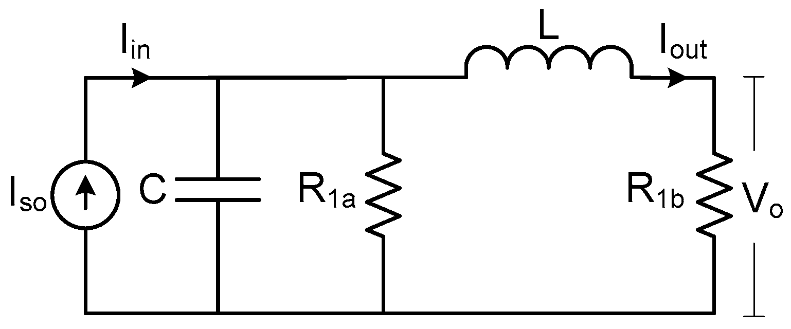
3.1. Review on the Single Mode Model
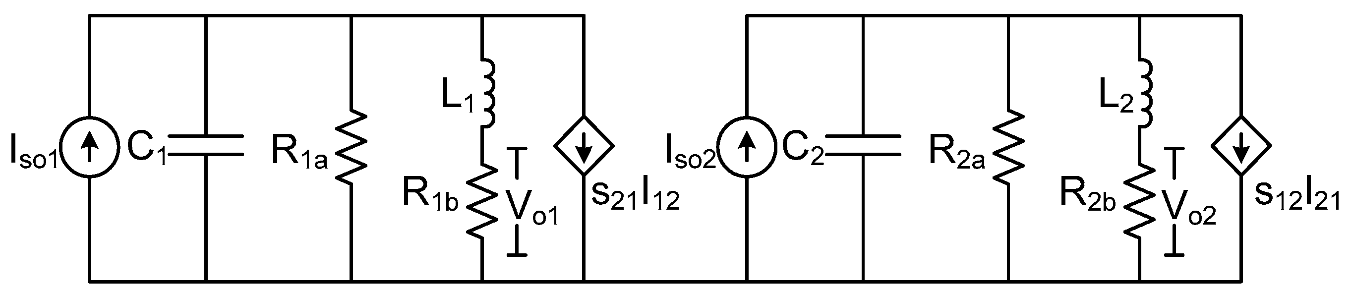
3.2. Two-Mode Model
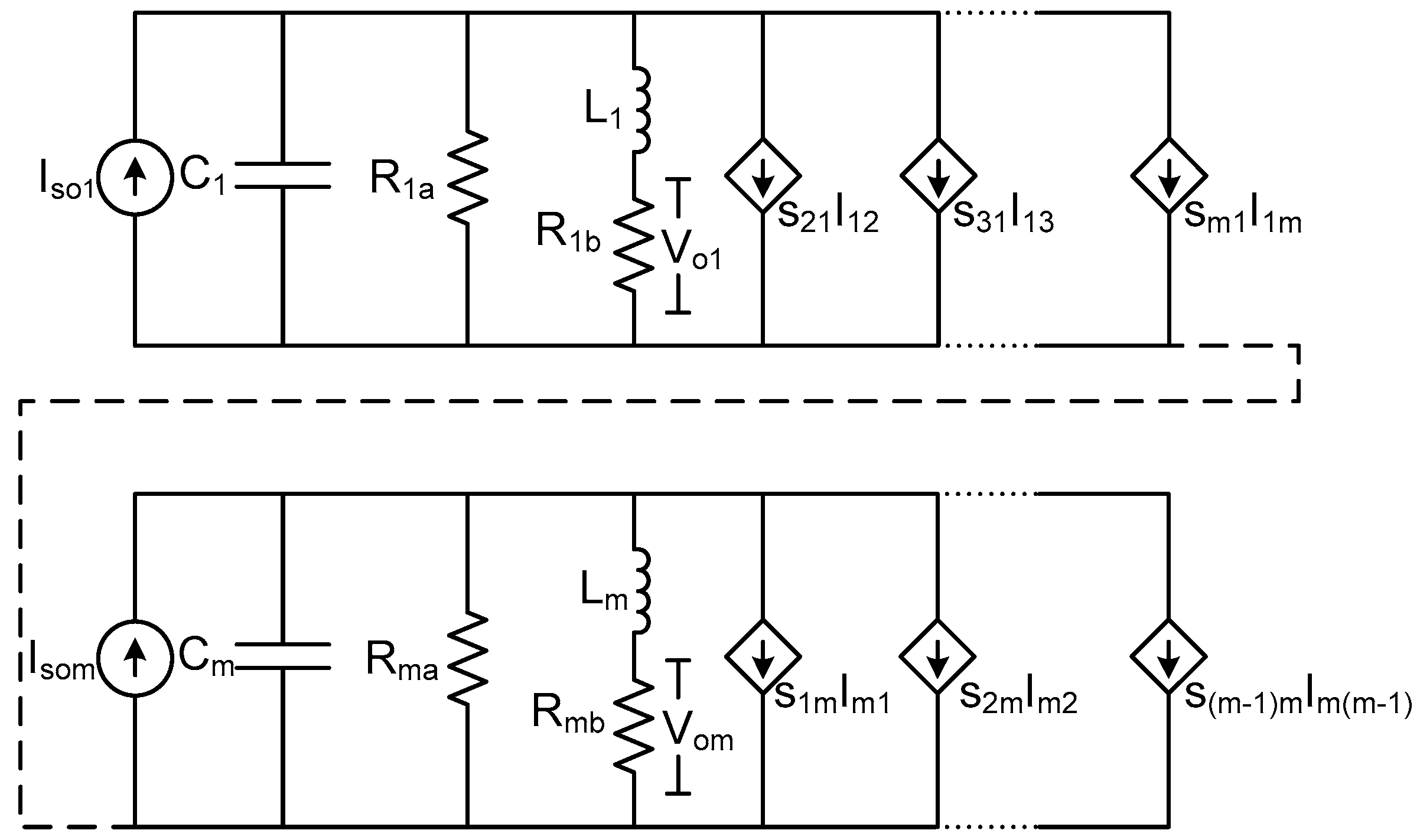
3.3. M-Mode Model
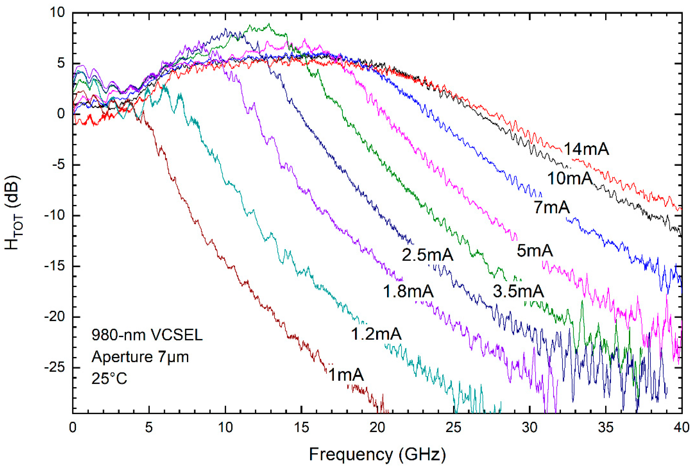
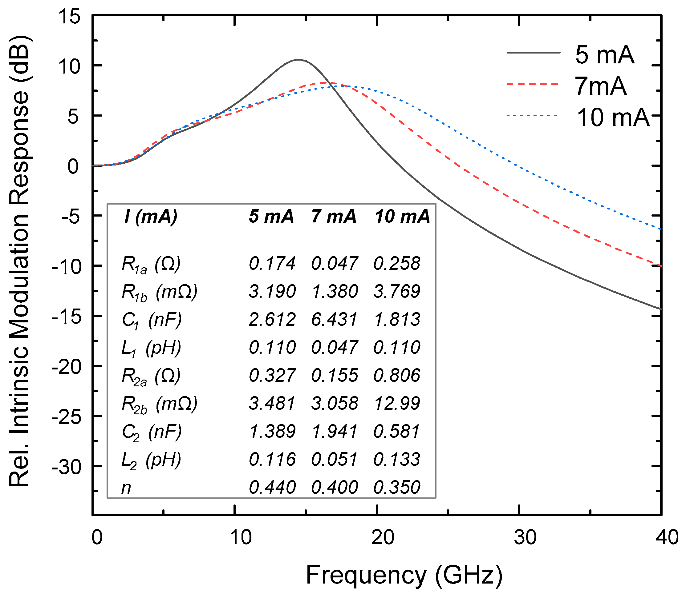
4. Circuit Simulation Results
5. Conclusions
Author Contributions
Funding
Acknowledgments
Conflicts of Interest
References
- Larsson, A. Advances in VCSELs for Communication and Sensing. IEEE J. Sel. Top. Quantum Electron. 2011, 17, 1552–1567. [Google Scholar] [CrossRef]
- Hofmann, W.; Bimberg, D. VCSEL-Based Light Sources—Scalability Challenges for VCSEL-Based Multi-100-Gb/s Systems. IEEE Photonics J. 2012, 4, 1831–1843. [Google Scholar] [CrossRef] [Green Version]
- Hamad, W.; Wanckel, S.; Hofmann, W.H.E. Small-Signal Analysis of Ultra-High-Speed Multi-Mode VCSELs. IEEE J. Quantum Electron. 2016, 52, 1–11. [Google Scholar] [CrossRef]
- Hamad, W.; Sanayeh, M.B.; Siepelmeyer, T.; Hamad, H.; Hofmann, W. Small-Signal Analysis of High-Performance VCSELs. IEEE Photonics J. 2019, 11, 1–12. [Google Scholar] [CrossRef]
- Gao, J. High Frequency Modeling and Parameter Extraction for Vertical-Cavity Surface Emitting Lasers. J. Lightwave Technol. 2012, 30, 1757–1763. [Google Scholar] [CrossRef]
- Tucker, R.S.; Pope, D.J. Microwave Circuit Models of Semiconductor Injection Lasers. IEEE Trans. Microw. Theory Tech. 1983, 31, 289–294. [Google Scholar] [CrossRef]
- Marozsák, T. Circuit Model for Multiple Transverse Mode Vertical-Cavity Surface-Emitting Lasers. J. Lightwave Technol. 2003, 21, 2977–2982. [Google Scholar] [CrossRef]
- Gao, J.; Li, X.; Flucke, J.; Boeck, G. Direct parameter-extraction method for laser diode rate-equation model. J. Lightwave Technol. 2004, 22, 1604–1609. [Google Scholar] [CrossRef]
- Coldren, L.A.; Corzine, S.W.; Mashanovitch, M.L. Dynamic Effects. In Diode Lasers and Photonic Integrated Circuits, 2nd ed.; John Wiley & Sons: Somerset, NJ, USA, 2012. [Google Scholar]
- Hamad, W.; Sanayeh, M.B.; Hamad, M.; Hofmann, W. Impedance Characteristics and Chip-Parasitics Extraction of High-Performance VCSELs. IEEE J. Quantum Electron. 2020, 56, 1–11. [Google Scholar] [CrossRef]
- Valle, A.; Pesquera, L. Theoretical calculation of relative intensity noise of multimode vertical-cavity surface-emitting lasers. IEEE J. Quantum Electron. 2004, 40, 597–606. [Google Scholar] [CrossRef]


© 2020 by the authors. Licensee MDPI, Basel, Switzerland. This article is an open access article distributed under the terms and conditions of the Creative Commons Attribution (CC BY) license (http://creativecommons.org/licenses/by/4.0/).
Share and Cite
Bou Sanayeh, M.; Hamad, W.; Hofmann, W. Equivalent Circuit Model of High-Performance VCSELs. Photonics 2020, 7, 13. https://doi.org/10.3390/photonics7010013
Bou Sanayeh M, Hamad W, Hofmann W. Equivalent Circuit Model of High-Performance VCSELs. Photonics. 2020; 7(1):13. https://doi.org/10.3390/photonics7010013
Chicago/Turabian StyleBou Sanayeh, Marwan, Wissam Hamad, and Werner Hofmann. 2020. "Equivalent Circuit Model of High-Performance VCSELs" Photonics 7, no. 1: 13. https://doi.org/10.3390/photonics7010013