1. Introduction
Semiconductor lasers have been used in fields of information communication and optical storage, taking advantage of the superior characteristics of compactness, high efficiency, and a long lifetime. However, as typical semiconductor lasers suffer from limited brightness (or power per unit area and unit solid angle), which is due to their operation in multiple longitudinal and lateral modes when increasing the emission area to enhance optical output, their application in the fields of material processing, sensing and measurement, and medical and life sciences has been hindered. Therefore, even now, large and complex lasers such as gas/solid/fiber lasers are necessary. If we could enhance the brightness of semiconductor lasers themselves by exceeding the limits of usual semiconductor lasers, a variety of laser-based systems could be simplified and made compact and inexpensive and have a large impact on a wide range of applications.
As new semiconductor lasers that principally enable the realization of high brightness, photonic-crystal surface-emitting lasers (PCSELs), which utilize the band-edge resonant effect and enable large-area coherent oscillation, have attracted considerable attention [
1,
2,
3,
4,
5,
6,
7,
8,
9,
10,
11,
12,
13,
14,
15,
16,
17]. The usage of band-edge resonance was proposed almost simultaneously and separately by our and other groups in 1999 [
1,
18]. In the other groups, Meier et al. reported lasing using a triangular-lattice photonic crystal and organic gain materials [
18]. However, their demonstrations did not show coherent two-dimensional (2D) oscillation, due to the lack of 2D coupling of light inside the photonic-crystal resonator at the band edges which they used (X- or M-point). In contrast, we have proposed a semiconductor laser utilizing the Γ-point of the triangular lattice [
1]. At the Γ-point, both 1D and 2D coupling occur; therefore, truly coherent oscillation can be obtained [
1,
3]. Moreover, the characteristics of the Γ-point enable emission in the surface-normal directions.
After the first demonstration of large-area coherent oscillation in PCSELs [
1,
3], a variety of functionalities and concepts have been demonstrated, such as the control of beam shapes and polarizations [
2,
7,
11,
12], the extension to shorter-wavelength (blue-violet) regions [
9], the addition of the functions of beam steering [
10,
15], and the realization of both high-beam-quality and high-power operation [
13]. Further, an approximately 10-W-class, high-beam-quality (M
2 ~ 2) laser was very recently realized [
16], demonstrating a brightness of about 300 MW cm
−2 sr
−1, which surpasses the limit of usual semiconductor lasers, by the development of a new type of photonic-crystal resonator. The continuous-wave (CW) output of this laser also reached about 7 W [
16].
In this article, we review the progress of PCSELs, which surpass the limit of traditional semiconductor lasers, including our proposal of a large-area coherent resonance in triangular-lattice PCSELs, the control of the beam pattern, the demonstration of beam steering, and recent high-power and high-beam-quality operation.
2. Large-Area Coherent PCSEL
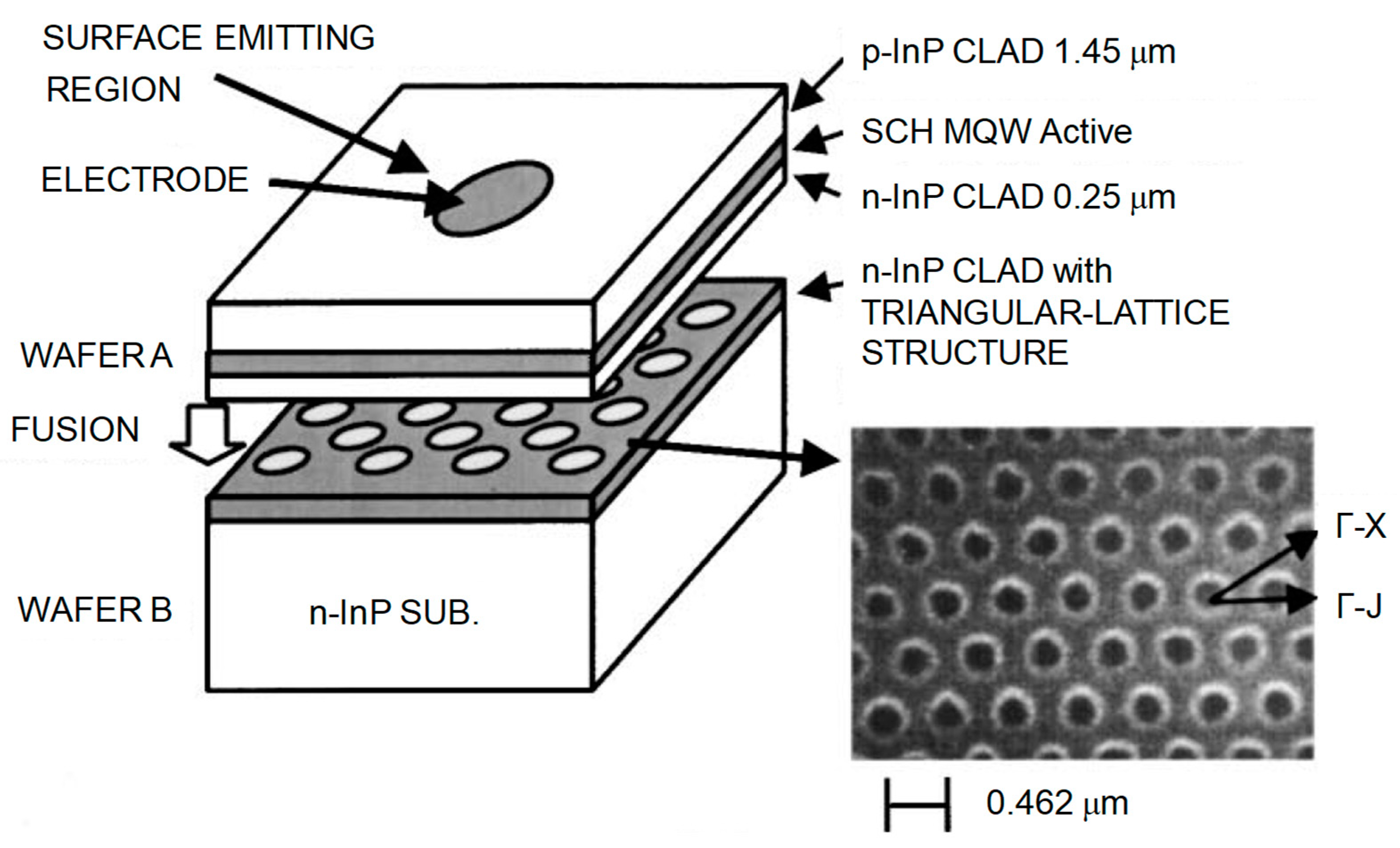
A schematic of the PCSELs with a triangular-lattice photonic crystal, which was proposed in 1999, is shown in
Figure 1 [
1,
3]. The devices at the early stages were fabricated by bonding two wafers to embed photonic crystals near an active layer. (We describe another fabrication method based on crystalline regrowth for high-power operation in
Section 5 and
Section 6.) In the first demonstration, we used InP-based semiconductors. On wafer A, we prepared a p-InP cladding layer and InGaAsP multiple-quantum-well (MQW) layers as the active layer. The emission wavelength of the MQW layers was about 1.3 µm. On wafer B, we prepared an n-InP cladding layer, and a triangular-lattice photonic-crystal pattern was fabricated by electron-beam (EB) lithography and reactive-ion etching techniques. The fabricated structure of the photonic crystal is shown in the scanning-electron microscope (SEM) image in
Figure 1. After the fabrication of the photonic-crystal patterns, the two wafers were pretreated by fluorine-based solutions to obtain clean surfaces, and then bonded via mass-transport phenomena during heat treatment. Subsequently, the unwanted substrate on the p-side was removed, and the p- and n-electrodes were prepared, enabling lasing under current injection. In this structure, the emitted light from the MQW is guided by the p- and n-cladding layers and the resonant effect of the photonic crystal, resulting in lasing. In addition, the photonic crystal induces diffraction in the surface-normal directions, emitting laser light around the p-type electrodes.
A photonic band diagram of the triangular-lattice photonic crystal calculated by the plane-wave expansion method is illustrated in
Figure 2a [
3].
Figure 2b shows the coupling states at the representative band edges I–IV: X-, J-, and first-order and second-order Γ-points [
3]. At the X-points (I), the coupling of the forward and backward light occurs one dimensionally. As the coupling between the light in different directions does not occur, three independent resonant states are formed. In addition, this band edge is non-radiative, because the in-plane wavenumber at the X-point is larger than that in air; thus, the light is confined inside the device due to total internal reflection. As a result, emission in the surface-normal directions is not expected. This point was employed by Meier et al. [
18] and is the reason why both 2D resonance and vertical emission were not obtained. The J-point (II) provides the coupling of three waves, whose directions differ by 120°, resulting in the formation of two independent resonant states. Therefore, we can use 2D resonant states; however, radiation in the vertical direction has not yet been obtained, because this band edge is non-radiative as well. In contrast to the X- and J-points, the Γ-point—particularly that of the lowest order (III)—provides 2D coupling of all six waves. Moreover, radiation in the surface-normal direction at the Γ-point is possible; therefore, its band edge is optimal for the resonance of surface-emission lasers. Here, an enlarged view of the band diagram around the lowest order Γ-point (III) is shown in
Figure 2c. As shown in this figure, this band edge is formed of six bands, two of which (B and D) are degenerate. We adjust the wavelength of this band edge to match the emission wavelength of the MQW, by tuning the lattice constant of the photonic crystal. For a MQW with an emission wavelength of 1.3 µm, we set the lattice constant to 462 nm (see
Figure 1).
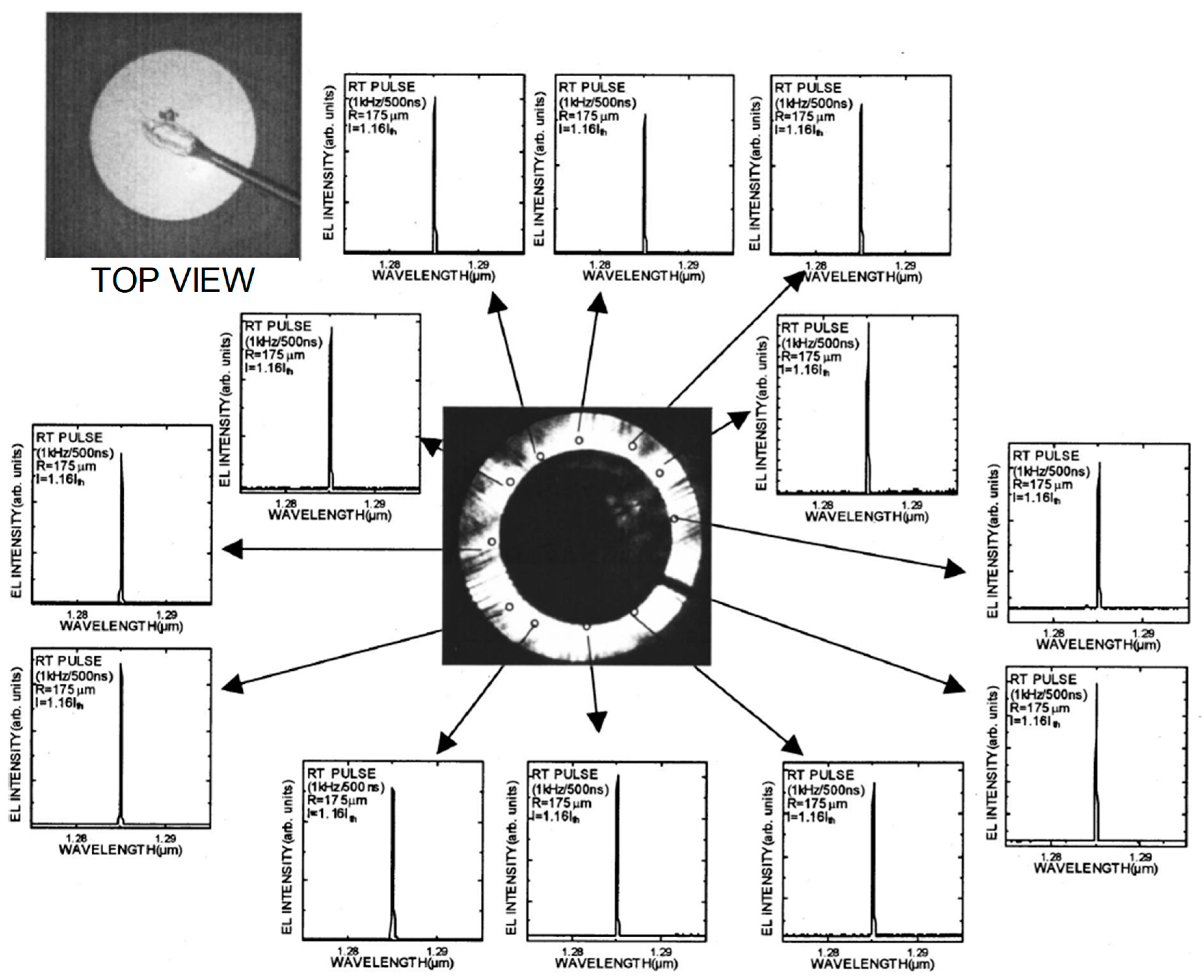
Lasing characteristics of the fabricated device are shown in
Figure 3 [
3]. The measurements were performed under pulsed operation (pulse duration of 1 kHz, pulse width of 500 ns). As shown in the near-field pattern (NFP) in the middle of
Figure 3, emission was observed around the p-electrode, whose diameter was ~350 μm (or, whose radius
R was ~175 μm). Spectra measured at several points (with an area of 15 µmΦ) are also shown in
Figure 3, revealing that lasing occurred at the same wavelength everywhere. This suggests that coherent oscillation over the broad area of the photonic crystal was successfully realized. Although we have heretofore explained the characteristics of PCSELs with triangular-lattice photonic crystals, we note that we have realized stable, large-area coherent lasing even at the Γ-point of a square-lattice photonic crystal [
7,
13,
16].
3. Control of Beam Patterns
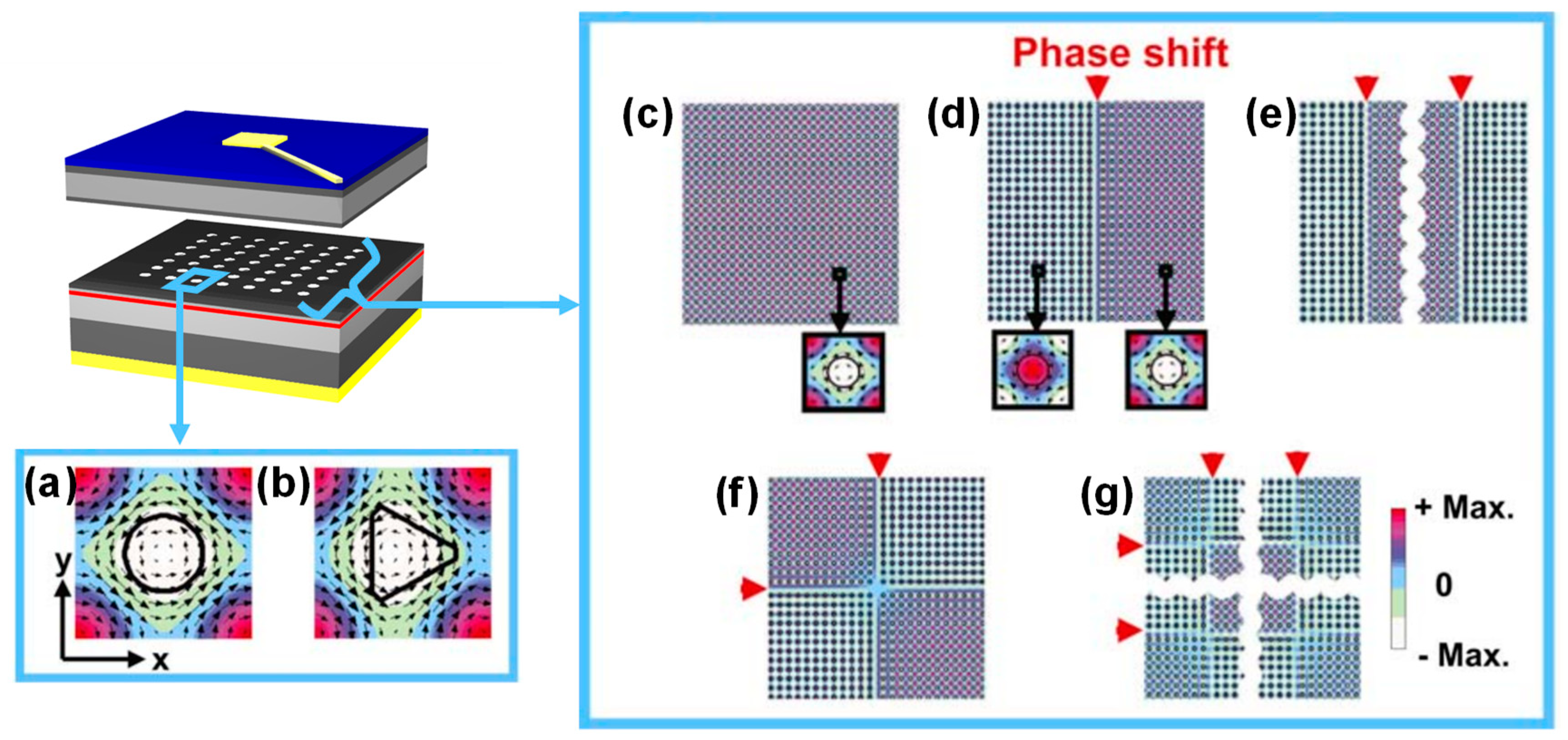
In semiconductor lasers, the beam patterns, or far-field patterns (FFPs), are expressed by the Fourier transformation of the electromagnetic field distribution at the near field. Therefore, by manipulating the electromagnetic field distribution of the lasing plane, the beam patterns can be controlled. For controlling the electromagnetic field distribution, we have proposed a method based on the modification of the shapes of the lattice points and the lattice phases between neighboring regions [
7]. Examples of electromagnetic field distributions of the Γ-point band edges of square-lattice photonic crystals are shown in
Figure 4 for some lattice-point shapes and phase shifts. In
Figure 4a,b we show the electromagnetic field distribution within a unit cell for the cases of lattice points with circular and triangular shapes, respectively. From the figure, we find that when the lattice points have a circular shape, symmetric electric fields centered at the middle of the air hole are obtained. In contrast, when the shape is triangular, the symmetry of the electric field is broken because of the asymmetry of the shape of the lattice points in the x-direction. These modifications enable the change of optical coupling among the light waves propagating inside the photonic-crystal layer and emitted in the surface-normal direction.
Figure 4c shows the electromagnetic field distribution over a large area for the case without phase shifts, and
Figure 4d–g shows those when we introduce the shifts of lattice phases of 180° between certain areas. From
Figure 4d–g, we see that the introduction of lattice-phase shifts causes a phase difference of the electromagnetic field; therefore, the control of the in-plane distribution of the electromagnetic fields is achievable.
SEM images of fabricated square-lattice photonic crystal patterns based on the above discussion are shown in the left panels of
Figure 5a–f. Here, we have introduced such photonic crystals into devices fabricated by the wafer-bonding method using GaAs-based materials, which operated at a wavelength of around 980 nm. The area for current injection was 50 × 50 µm
2. The FFP of the device with circular air holes and no phase shift (
Figure 5a) was doughnut-shaped. This is because the electric field has rotational symmetry, as shown in
Figure 4a; therefore, the electric field is cancelled out around the center of the device. This symmetry is broken when the lattice shape is triangular (
Figure 4b), resulting in the suppression of destructive interference and thus the emission of single-lobed output beams, as shown in
Figure 5f. The introduction of asymmetry is important to obtain efficient light extraction to the surface-normal direction; that is, asymmetry is also essential for realizing high-power operation (which we address in
Section 5). The effect of the introduction of phase shifts is clearly seen in
Figure 5b–e where two or four doughnut shapes were obtained because of the change in interference between phase-shifted regions. These are the results of in-plane coherence and the uniformity of the wavelength of a photonic crystal laser.
4. Beam Steering by PCSELs
Technological advancements for scanning laser beams have attracted much attention for applications such as laser sensing (LiDAR), head-mounted displays, projection, and scanning. So far, the scanning of laser beams has been achieved by using auxiliary, movable mirrors. However, these mirrors, mechanical in nature, suffer from a limited scanning speed and low reliability. To overcome the limitations of mechanical systems, we have developed a new beam-steering technique using one-chip semiconductor lasers, where we assemble an array of PCSELs, each of which emits a laser beam in a unique direction and drive them electronically [
10,
15]. This fully electronic system is expected to enable fast (~GHz) and reliable scanning of laser beams.
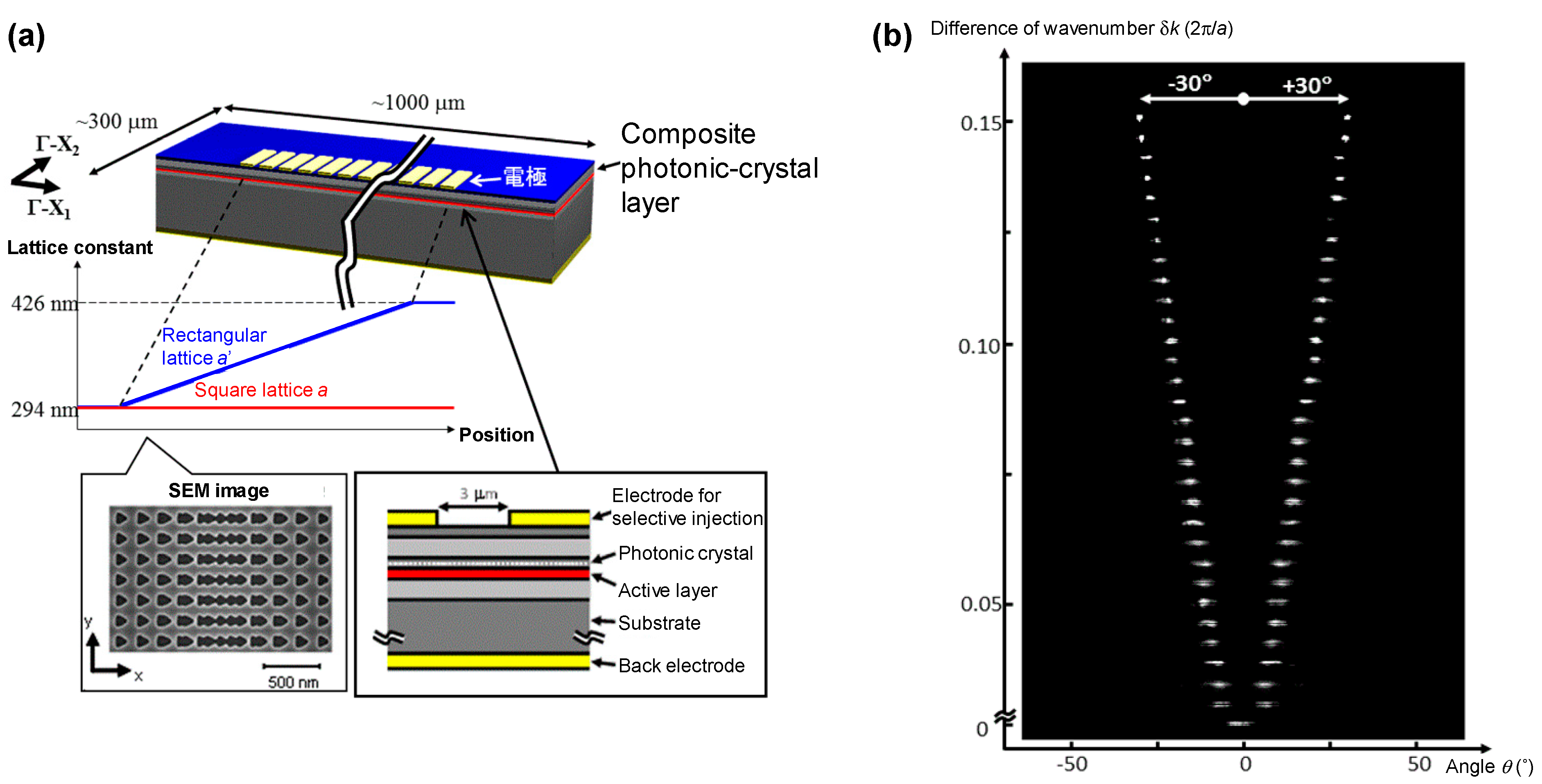
To obtain laser emission in a targeted direction, we first designed a new photonic-crystal structure, by which an artificial lasing band edge was generated at a finite in-plane wavenumber that determines the resonant condition and output direction [
10]. Specifically, we designed composite photonic-crystal structure with overlapping square and rectangular lattices, as shown in
Figure 6. As shown in
Figure 6a,b, in a normal square-lattice photonic crystal, the band edge at which resonance occurs is formed at the Γ-point as discussed above. At the Γ-point, the in-plane wavenumber equals zero, so laser emission occur in the surface-normal direction. However, when we overlaid the square and rectangular lattices, as shown in
Figure 6c, new band edges appeared at an in-plane wavenumber shifted away from the Γ-point, as shown in
Figure 6d. At these new band edges, the in-plane wavenumber is finite, so emission deviates from the surface-normal direction. In detail, when the lattice constant of the square lattice and rectangular lattice is
a and
a’, respectively, the band edges appear at an in-plane wavenumber shifted by δ
k = π(1/
a − 1/
a’) from the Γ-point; in terms of the beam direction, emission is obtained at an angle of
θ = sin
−1(δ
k/
k0), where
k0 = 2π/
λ, from the surface normal.
Based on this concept, we have developed a device, as shown in
Figure 7a. The photonic crystal of this device was composed of a square lattice with a fixed lattice constant
a and a rectangular lattice whose lattice constant
a’ was gradually changed along the length of the photonic crystal. Electrodes were arrayed in one dimension in order to selectively drive different regions of the photonic crystal.
Figure 7b shows the experimental results of 1D beam steering. With this device, we successfully demonstrated the control of the emission direction over a range of ±30° from the surface normal. Moreover, although
Figure 7b only shows the results of a discrete (coarse) change of output direction, we also succeeded in a continuous (fine) tuning by controlling the balance of injected currents of neighboring electrodes.
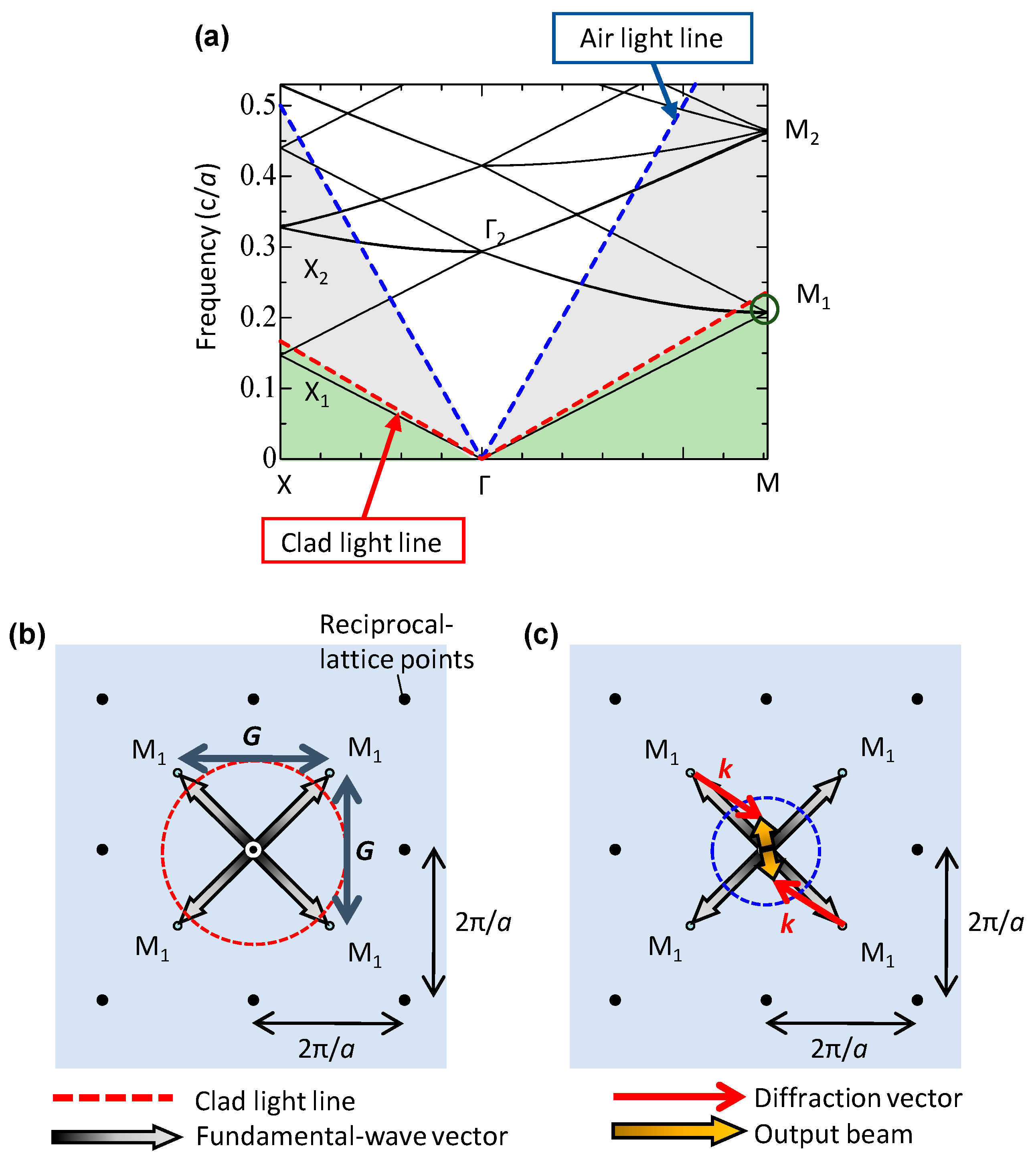
As introduced above, the first demonstration of beam steering was realized using composite photonic crystals. However, this method has been essentially limited to 1D steering because of the usage of the difference of lattice constants between square- and rectangular lattices. In addition, as the resonant band edges are changed depending on the emission angle, lasing characteristics also change when changing emission angle. Considering these issues, we recently investigated another way to obtain oblique-angle emission, where we use 2D resonance at a non-radiative band edge and an additional diffraction into a targeted direction [
15]. The non-radiative band edge we used is the M-point of a square lattice, shown in
Figure 8a. Similar to the J-point of a triangular lattice as discussed in
Section 2, propagating in-plane light waves, of which there are four at the M-point, can couple two-dimensionally as illustrated in
Figure 8b. Here, if we could introduce diffraction vector
k as shown in
Figure 8c, light can diffract within the air-light line with a finite in-plane wavenumber, resulting in emission at an oblique angle.
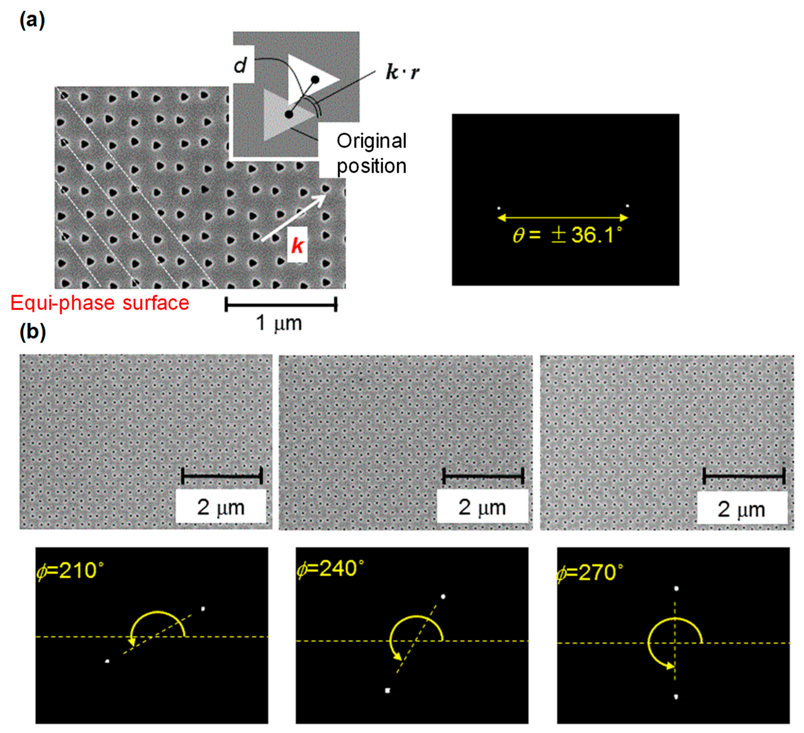
To introduce this diffraction vector
k, we proposed a square-lattice photonic crystal with modulated lattice points.
Figure 9a shows a SEM image of one such modulated photonic crystal, whose lattice points are shifted from their original position by a distance of
d at an angle of
Ψ(
r)
= k·r. In
Figure 9a, the lattice constant
a was 208 nm, and the modulation distance
d was 0.1
a. The experimental FFP in
Figure 9a shows that the output beam was successfully emitted as designed. We also demonstrated emission within a range of
θ = ±45°. Here, it is noteworthy that the diffraction vector created by the modulated photonic crystal can be tuned two-dimensionally; that is, the control of the azimuth angle
ϕ is achievable;
Figure 9b shows a demonstration of this control with several examples. These results show that the 2D control of the emission direction is possible. A proof-of-concept demonstration of (L-shaped) beam scanning based on this concept was successfully carried out [
15]. It is expected that dynamic 2D beam scanning will be achieved by arraying modulated photonic crystals and driving electrodes in two dimensions and then electrically switching between these driving electrodes.
5. High-Beam-Quality and High-Power PCSELs
Recently, high-beam quality and high-power lasers have increased in importance in fields such as material processing, sensing, and medical applications. In this section, we review the progress in obtaining high-power operation in devices operating in the near-infrared region (wavelength ~ 1 µm). To obtain high-power GaAs-based lasers, we developed an air-hole-retained regrowth method [
13]. The employment of crystalline regrowth is useful for avoiding the formation of undesired interfaces between regions of discontinuous crystallinity, which was unavoidable when we used the wafer bonding method (
Section 2). As a result, high-power emission, including CW operation, with suppressed, unwanted heating during high current injection was achieved. In addition, as the sufficient extraction of light in the surface-normal direction is necessary to obtain a high power, we have employed asymmetric lattice-point shapes, i.e., a right-angled triangle, in square-lattice photonic crystals [
13]. Here, an epitaxial-regrowth method to completely fill the etched structure was also investigated [
14]. Using this method, the 1D and 2D coupling coefficients of the fabricated devices became lower than those of the devices fabricated using air-hole-retained regrowth due to the lower refractive index contrast, which might reduce the stability of oscillation.
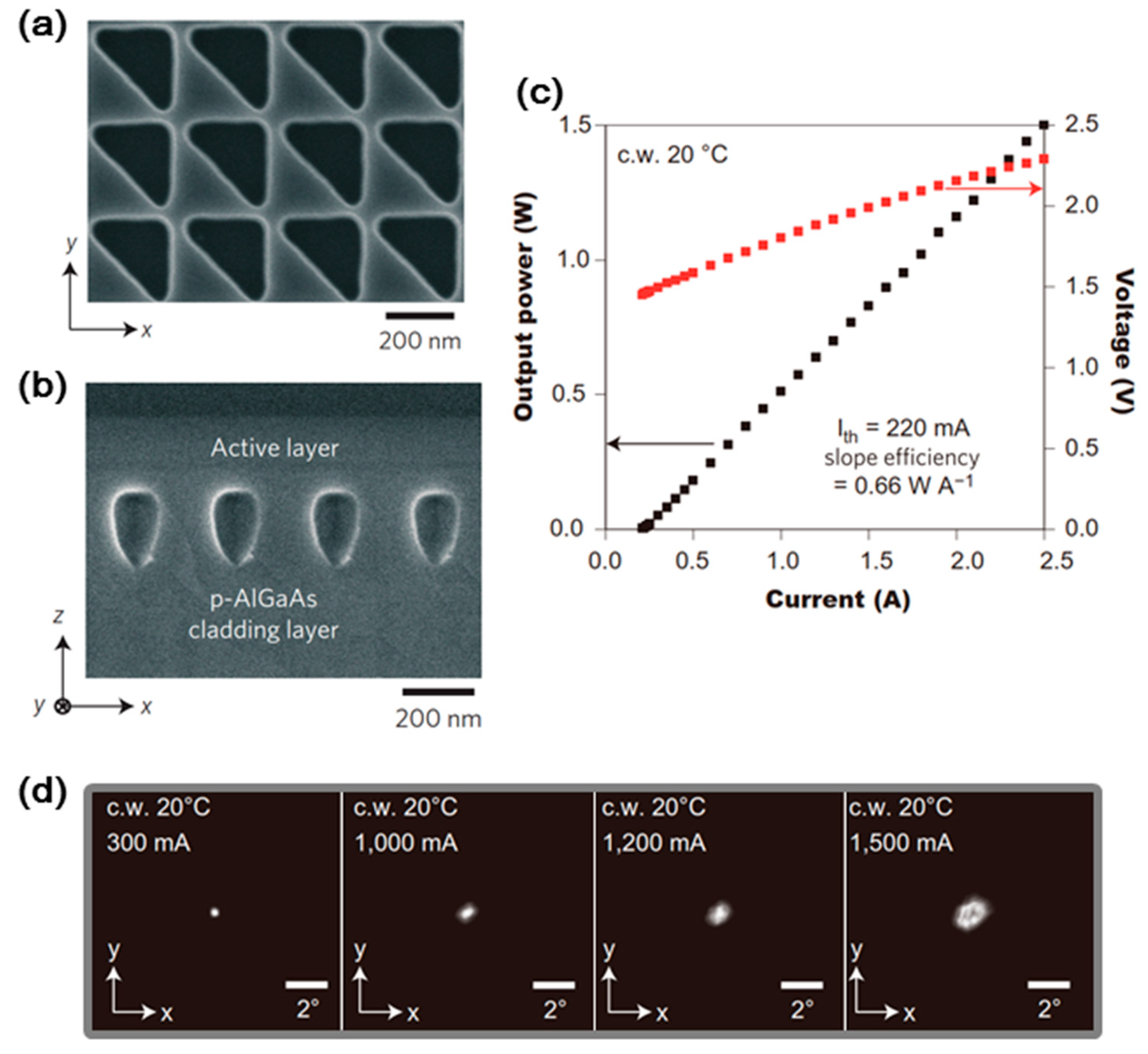
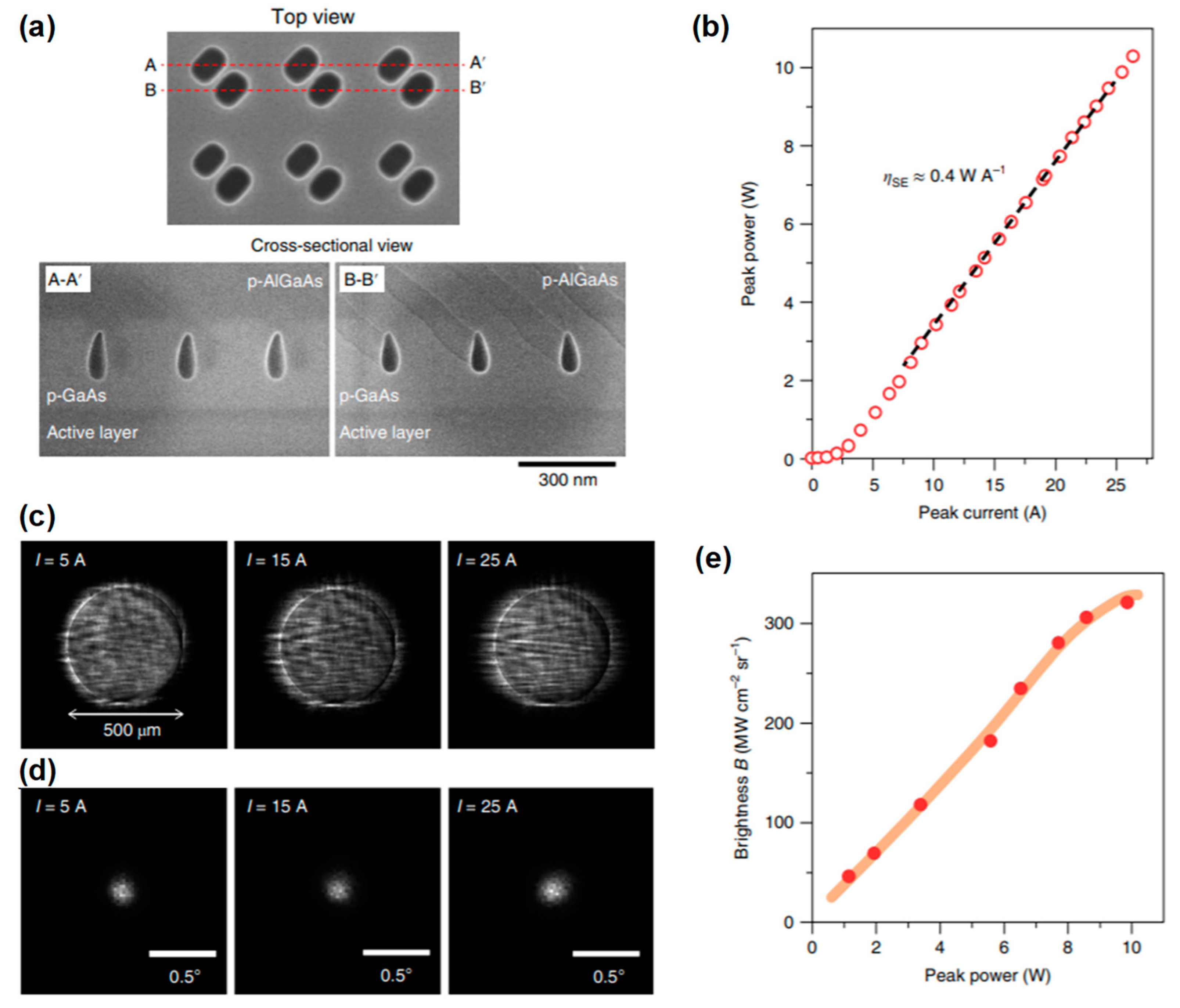
In the fabrication of the devices, we first grew n-AlGaAs as a cladding layer and an InGaAs/AlGaAs MWQ and p-GaAs for preparing photonic crystals on a n-GaAs substrate. On this wafer, we then fabricated a square-lattice photonic crystal with right-angled triangular lattice points by EB lithography and dry etching. The top-view SEM image after dry etching is shown in
Figure 10a. Here, the lattice constant was set to 287 nm to align the resonant wavelength at the Γ-point band edge to the emission wavelength of the MQW. Subsequently, the p-AlGaAs cladding layer and p-GaAs contact layer were grown on the photonic crystal pattern. Here, for obtaining retained air holes in the GaAs-based system, we developed a new regrowth method utilizing the nature of different growth rates depending on the crystalline facets. As a result, as shown in
Figure 10b, we succeeded in the formation of air holes near the active layer [
13]. Finally, a p-electrode was prepared to make the injecting areas 200 × 200 µm
2. In addition, we introduced a device structure in which the laser emission could be efficiently extracted without being masked by a p-electrode; namely, we added a window-shaped n-electrode and attached the device to a heat sink with the p-electrode face-down.
Figure 10c shows the I–L characteristics under CW operation. From the figure, we see that a low threshold current of 220 mA and high slope efficiency of 0.66 W/A were achieved, and a high output power of 1.5 W was realized.
Figure 10d shows the FFPs for different injection current levels. At an output of 0.5 W (~1 A), the divergence angle was less than 0.5°, suggesting operation with a very high beam quality. Even though the divergence angle increased when the injection levels became high, this might be due to the appearance of a distribution of the refractive index, which was induced by a temperature distribution caused by heating during CW current injection. The reduction, or compensation, of this temperature distribution would improve the output beam pattern even under higher CW output.
Toward higher brightness, a new photonic-crystal resonator, which enables the photonic-crystal area to be enlarged while maintaining the high beam quality, was very recently developed [
16]. To obtain high-beam-quality oscillation even in large-area PCSELs, it is crucial to realize a selective oscillation in the fundamental mode, where the light intensity is distributed around the center of the resonator with a unimodal profile, while suppressing the oscillation in multimodal higher-order modes, where the light intensity also exists around the edge of resonator. However, in usual photonic-crystal structures, when enlarging the resonant area, the field intensity of both the fundamental and higher-order modes decrease at the edge of resonator; therefore, the in-plane leakage loss of both the modes decreases. This results in the reduction of their threshold gain margin and induces the issue of multimodal oscillation. To overcome this issue, it is important to adequately weaken the in-plane confinement. Upon doing so, the light intensity will spread over the entire resonator both for the fundamental and higher-order modes; as a result, the in-plane loss of the higher-order mode will increase relative to the fundamental mode and the lasing in these unwanted modes will be suppressed.
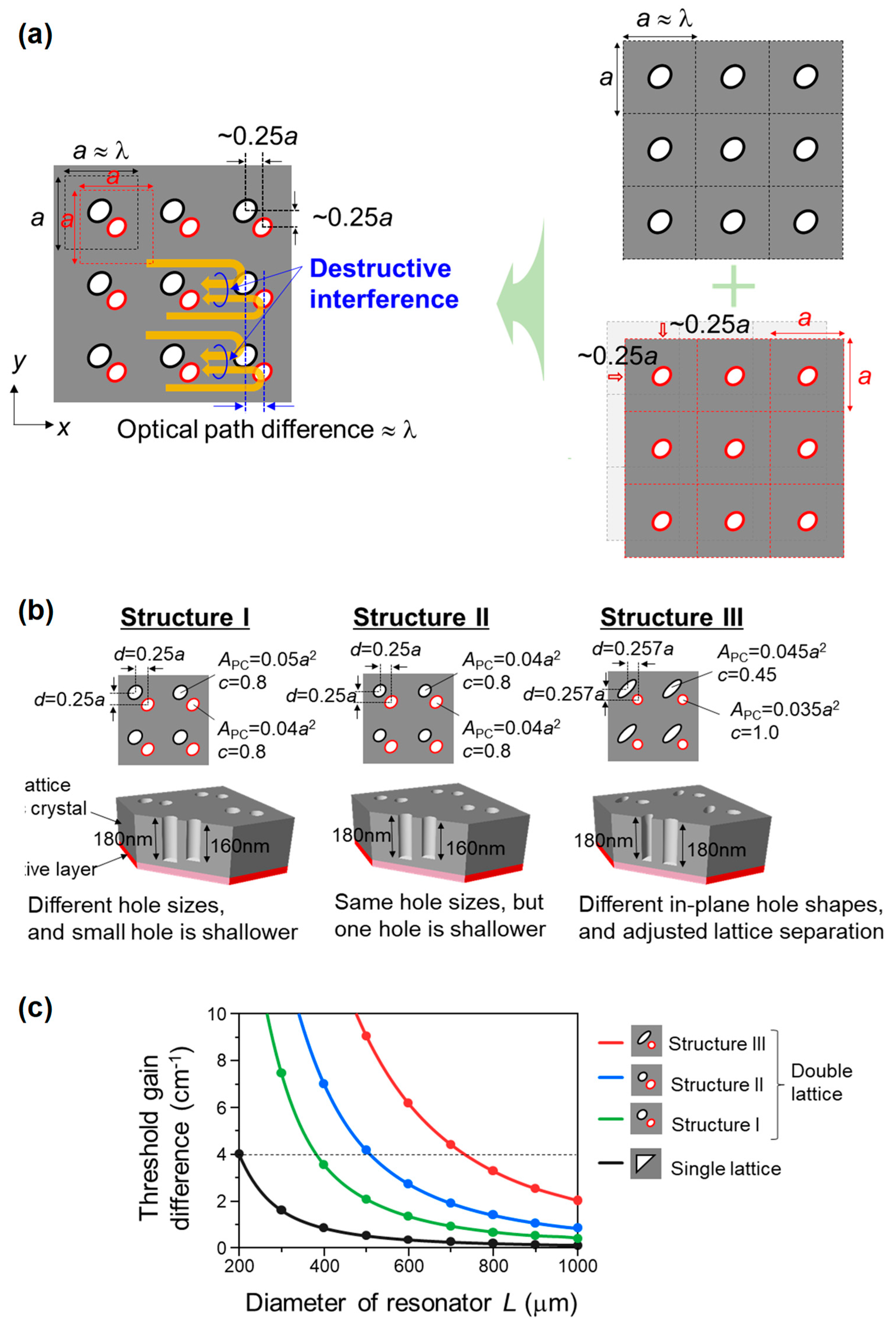
Based on this concept, we designed “double-lattice” photonic crystals, where two square-lattice photonic crystals are overlaid with a shift of 1/4 in wavelength, or 1/4 in lattice constant, as shown in
Figure 11a [
16]. In this structure, the difference in the optical length between the light diffracted in the 180° direction by the two lattices equals half the wavelength. This induces destructive interference of such diffracted light by the two lattices; therefore, the in-plane confinement effect can be adequately weakened. Here, it is also important to consider the vertical radiation in such a double-lattice structure. As a completely balanced double lattice has a high degree of symmetry, similar to the normal square-lattice with circular air holes (
Figure 5a), the vertical radiation will be strongly suppressed. To avoid this, we have introduced asymmetry by giving each of the two lattices different air-hole filling factors, heights, and shapes, as shown in
Figure 11b (Structure I, II, III). The results of the calculation of the threshold-gain margin between the fundamental and higher-order modes for the three types of designed double lattices, as well as the single lattice, shown in
Figure 10, are presented in
Figure 11c. These calculations were performed by using 3D coupled wave theory [
19,
20]. From the figure, we find that double lattices enable a sufficient threshold-gain margin to be maintained even when increasing the device size. Using the 200-µm single-lattice device, which achieved high-beam quality operation with a threshold-gain margin of about 4 cm
−1, as a benchmark, the double-lattice structures I, II, and III are expected to enable an increase in device size to 300, 500, and 800 µm, respectively, with similarly high beam qualities. This implies that double lattices can increase the area of the resonator by a factor of 5–10 over that of single lattices.
Figure 12a shows the fabricated double-lattice photonic crystals (structure II) based on the metal–organic vapor phase epitaxy (MOVPE) regrowth technique using an organic-arsenic source [
21,
22]. Here, to obtain a double-lattice structure with a height difference, as shown in structure II (
Figure 11b), we first performed two-step etching to prepare holes with different heights, and then performed crystalline regrowth. Cross-sectional SEM images shown in
Figure 12a show that the difference in air-hole height was adequately maintained after the regrowth. A calculation using the experimental air-hole shape also revealed that the threshold-gain margin was expected to be more than 4 cm
−1 at the device size of 500 µm. Moreover, the calculation showed that the radiation coefficient in the surface-normal direction was about 20 cm
−1.
Figure 12b shows the measured operation characteristics of a device with a p-electrode of 500 µmΦ driven by a pulsed current with a pulse width of 200 ns [
16]. As shown in
Figure 12b, an output power exceeding 10 W was successfully obtained. In this device, the slope efficiency was about 0.4 W/A, and was restricted by undesired emission toward the direction opposite to the output, i.e., toward the p-electrode, which resulted in a loss. This undesired emission can be recycled by introducing a reflector, such as a distributed Bragg reflector, between the photonic-crystal layer and p-electrode, upon which the slope efficiency is expected to improve to more than 0.7–0.8 W/A. The measured NFPs and FFPs at different injection currents (
Figure 12c,d) show that a single-spot beam with a very narrow divergence angle (less than 0.3° estimated from the 1/
e2 width) was emitted over the entire 500-μm-diameter injection current region. These results indicate that broad-area coherent lasing was realized. Furthermore, as shown in
Figure 12e, which displays the dependence of the estimated brightness on the power, a very high brightness exceeding 300 MW cm
−2 sr
−1 was realized, which is the highest level of brightness achieved using semiconductor lasers.
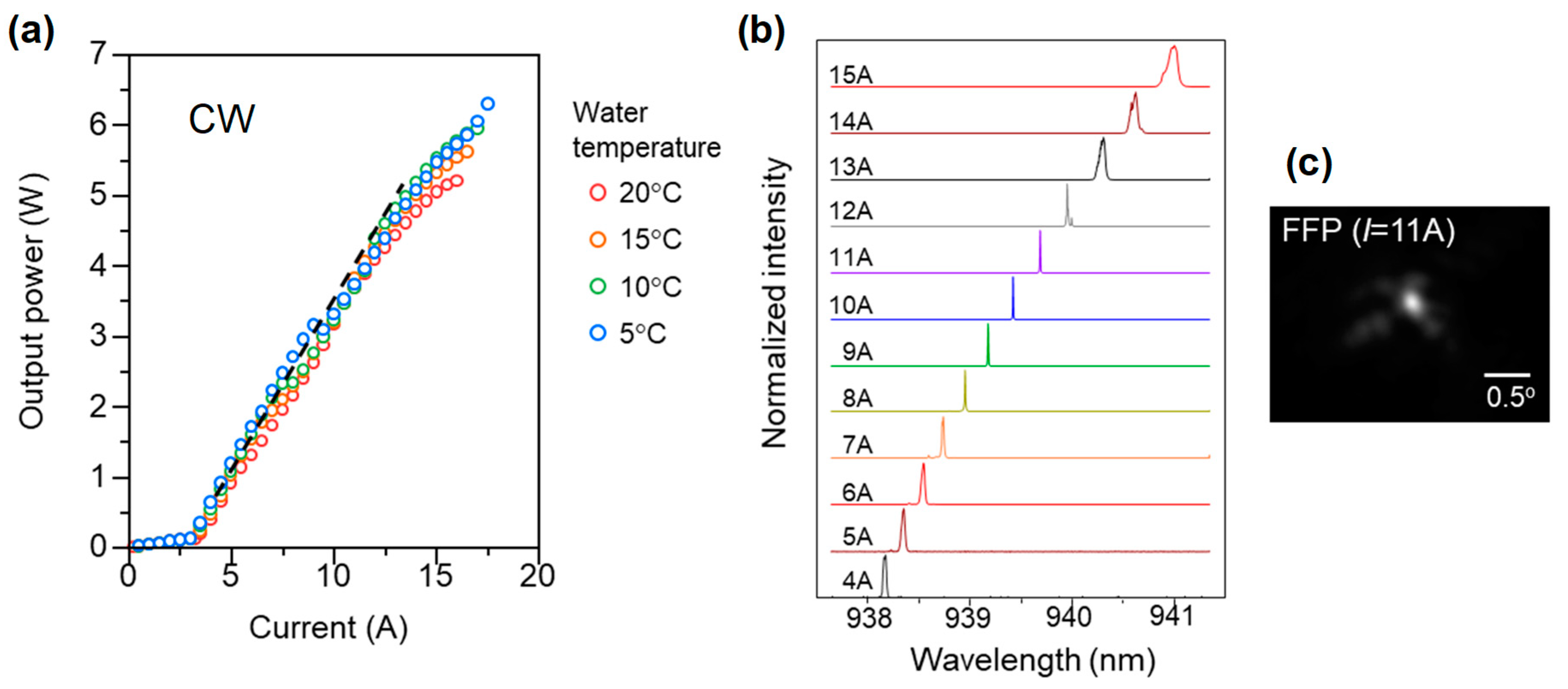
Furthermore, we fabricated a device with double-lattice structure III, which is suitable for a device with a p-electrode-diameter of 800 μm, and demonstrated CW operation (
Figure 13). The device chip was mounted on a water-cooling package via a sub-mount with a high thermal conductance to obtain sufficient heat dissipation. As a result of measuring the I–L characteristics, a CW output reaching about 7 W was successfully obtained. The FFP shows that the beam divergence was less than ~0.2°, measured using the 1/
e2 width.


