Article

Photonic Crystal Circular Defect (CirD) Laser †

Graduate School of Engineering, Osaka University, 2-1 Yamada-oka, Suita, Osaka 565-0871, Japan
*
Author to whom correspondence should be addressed.
Invited Paper.
Photonics 2019, 6(2), 54; https://doi.org/10.3390/photonics6020054
Submission received: 26 April 2019 / Revised: 17 May 2019 / Accepted: 18 May 2019 / Published: 20 May 2019
(This article belongs to the Special Issue Photonic Crystal Laser and Related Optical Devices)

Abstract

:
We describe the design of photonic crystal circular defect (CirD) lasers to construct a compact optical module with a wavelength division multiplexing function for the application of inter-chip or intra-chip optical interconnects. Subsequently, we investigated the characteristics of CirD lasers including the quality factor of the cavity, the lasing threshold, and the modulation speed with a three-dimensional finite-difference time-domain method and two-dimensional rate equations. Finally, we demonstrated the single mode lasing and wavelength tuning behaviors of the CirD lasers using optical pumping technology under room-temperature continuous-wave conditions.

1. Introduction

Conventional copper-based electrical interconnects have increasing difficulty keeping up with the present rate of progress of inter-chip or intra-chip communications [1]. Optical interconnects using silicon (Si) photonic technology are currently the strongest candidate to address this bottleneck due to their exceptional potential for higher bandwidth, lower energy consumption, and lower latency [2,3,4,5]. For inter-chip interconnects, the required bandwidth density is expected to reach approximately 10 Tbps/cm2 [6]. Recently, a silicon photonics optical transceiver with a high bandwidth density of 0.4 Tbps/cm2 was demonstrated [7], and substantial improvements are expected with more refined designs and advanced technologies. However, for intra-chip optical interconnects, larger numbers of CPU cores will be integrated on one chip as complementary metal oxide semiconductor (CMOS) scaling continues in the future, and it will become necessary to provide high bandwidth of 1 Tbps (10 Gbps × 100 cores) within a space of approximately 1 × 10 4 cm2 [8]. To meet such bandwidth density demands of approximately 10 Pbps/cm2, optical components have to offer high capacity, high energy efficiency, and low cost.
A platform consisting of Si and silicon oxide itself is well suited for constructing various photonic components, such as waveguides [9,10], modulators [11], and photodetectors [12]. However, achieving an efficient electrically-driven light source on Si remains challenging due to the indirect bandgap of Si. A promising solution is the heterogeneous integration of III-V lasers on Si [13]. However, traditional III–V lasers such as distributed-feedback (DFB), distributed Bragg reflector (DBR), and vertical cavity surface-emitting lasers (VCSEL) have difficulty satisfying high bandwidth density demand. Photonic crystal (PhC), due to its unique physical properties resulting from the photonic bandgap [14], has been intensively researched [15,16,17]. PhC-based optoelectrical devices have shown excellent performance in terms of energy efficiency and operation speed [18,19,20,21]. Therefore, the heterogeneous integration of PhC lasers on Si is an attractive means to achieve a light source for inter-chip or intra-chip optical interconnects. Recently, using direct bonding and buried regrowth technologies on a silicon-on-insulator substrate, lambda-scale embedded active-region photonic-crystal (LEAP) lasers showed a low threshold current of 24 μA and an extremely low energy cost of 7.3 fJ/bit at bit rates of 10 Gbps under continuous-wave (CW) room-temperature (RT) conditions [22]. The maximum output power of the on-silicon LEAP lasers was as low as 450 nW at an injected current of 500 μA, which includes approximately 10 dB of optical coupling loss between the Si waveguide and the fiber [22]. In contrast, the heterogeneously-integrated DFB and DR lasers on Si exhibited three orders of magnitude higher output power of approximately 0.7 mW [23]. For practical applications to future optical interconnects, increasing the output power is critical for on-silicon LEAP lasers.
We previously proposed a novel electrically-driven PhC laser structure [24] called the CirD laser since a circular-defect cavity that forms a whispering gallery mode (WGM) along the cavity boundary is used to generate the laser light in this structure [25]. By simultaneously employing two AlGaAs/AlGaOx cladding layers, CirD lasers enable RT-CW operation through vertical current injection. The most important advantage of CirD lasers is that they can control the lasing wavelength by simply adjusting the radius of the cavity (R) while maintaining a high quality factor (Q) [26]. Therefore, integrating several cavities with different R to only one PhC line-defect waveguide can achieve a monolithic integrated laser array that enables wavelength division multiplexing (WDM) without a conventional optical multiplexer. This architecture can also be used to construct a CirD photodiode (PD) array. Thus, monolithically fabricating the laser and PD arrays on one chip can achieve an optical module with an extremely high bandwidth density. We estimated the operation speed of one CirD cavity at approximately 50 Gbps due to the small cavity size. Therefore, if 20 cavities are integrated with one waveguide in both the CirD-laser and CirD-PD arrays, the bandwidth density is expected to reach 10 Pbps/cm2. In addition, due to its small footprint, millions of such modules can be produced from a 6-inch GaAs wafer. Thus, this optical module can also address low cost requirements.
In this paper, we report the recent development of CirD lasers. In Section 2, we present a detailed design of CirD lasers for WDM. Section 3 reports the numerical analyses of CirD lasers using the three-dimensional (3D) finite-difference time-domain (FDTD) method and two-dimensional (2D) rate equations. In Section 4, a proof-of-principle experiment of the wavelength tuning of CirD lasers is conducted using optical pumping. Finally, a brief summary is given in Section 5.

2. Design of Cird Lasers for Inter-Chip or Intra-Chip Optical Interconnects

2.1. Cird Laser Structure

Figure 1 shows a schematic birds-eye-view image of the CirD laser structure. The GaAs core layer is sandwiched by two AlGaAs/AlGaOx cladding layers, and a GaAs contact layer is placed on top. The AlGaOx are fabricated by selectively oxidizing the AlGaAs through air holes, and the AlGaAs at the cavity center are preserved to form a funnel that transports the currents. Using AlGaAs/AlGaOx cladding layers offers advantages such as efficient vertical current injection, high thermal conductivity [16], and high mechanical stability, all of which allow the CirD lasers to operate under RT-CW conditions. However, due to the low index contrast between the GaAs core and AlGaOx cladding layers, the light confinement of CirD lasers in the vertical direction is weaker than that of other PhC lasers with an air-bridged structure. This issue is solved by the circular-defect cavity that was formed by 18 symmetrically-distributed air holes. A WGM that is also observed in micro-disk lasers can be formed along the cavity boundary of the CirD lasers. However, micro-disk lasers suffer from the issue of mode selectivity, i.e., several WGMs with different azimuthal mode numbers can be formed in the micro-disk lasers because there is no limitation at the pure circular cavity. In contrast, since the cavity boundary of the CirD lasers is in the geometry of a gear, only one WGM matching this geometry can be generated in the cavity with nine periods (Figure 2). 18 high-intensity WGM lobes were distributed along the cavity boundary, and the WGM’s electromagnetic energy at the cavity center is almost zero. Thus, AlGaAs/AlGaOx cladding layers provide a unique approach to the use of WGM: utilizing AlGaOx to cover the lobes and AlGaAs to transport currents. Considering the trade-off between the vertical photon confinement and the cross-section of the AlGaAs funnel, the optimized AlGaOx width, i.e., the oxidation width penetrated from the sidewall of the air holes, is 0.8 a, where a is the lattice constant of the triangular lattice. In addition, due to the modal cancellation effect, little WGM energy is radiated into the vertical directions. Therefore, CirD lasers offer an adequate Q for lasing even with AlGaAs/AlGaOx cladding layers.
For optical communications applications, CirD lasers with a GaAs material system aim for the 1.3-μm range. Thus, GaInNAs quantum wells (QWs) and InAs quantum dots (QDs) are suitable material candidates to provide optical gain. GaInNAs QWs offer a higher model gain relative to InAs QDs, but have a larger non-radiative recombination rate at the sidewall of the air holes that considerably influence the lasing operation. In contrast, InAs QDs have the following advantages: a low non-radiative recombination rate, a low temperature dependence, and a low transparent carrier density.
In CirD lasers, a PhC line-defect waveguide coupled with the cavity is used to output the laser light. Figure 2 shows a mode profile when the WGM is coupled with the waveguide mode, which is calculated by the 3D FDTD method. The coupling efficiency η between WGM and waveguide mode is defined as
η = 1 Q 1 Q s 1 Q ,
where 1 Q indicates the energy loss rate through the cavity and the waveguide and 1 Q s indicates the energy loss rate of the solo cavity structure without a waveguide [27]. In the practice design of CirD lasers, η is tuned to achieve high power and high modulation speed while maintaining a low threshold.

2.2. Monolithic Optical Module Architecture

To meet the high bandwidth density requirements of future optical interconnects, WDM technology, which transmits multiple wavelengths through the same waveguide, will be used to scale up the aggregate transmission capacity. However, since traditional WDM technology with optical multiplexers needs a large footprint, novel architecture is required when the regime addresses the chip level. Since CirD lasers can simply tune the lasing wavelength by adjusting the cavity’s radius, they offer a promising approach to address this issue. Figure 3a shows a CirD laser array architecture that enables WDM applications without the need of an optical multiplexer. 20 CirD cavities with different lasing wavelengths are arranged on both sides of one PhC line-defect waveguide. Since the value of a is approximately 360 nm, the distance between two adjacent cavities is set to 5 μm. Each cavity is surrounded by more than ten PhC lattice periods that provide sufficient light confinement in the horizontal direction. The laser array that handles 20 wavelengths only needs a length of 100 μm.
In CirD lasers, the vertically-injected currents are horizontally diffuse to adjacent cavities through the top GaAs contact layer. They must be electrically isolated to independently control the cavities. Since the AlGaOx is insulated, the above issue is solved by selectively etching the GaAs contact layer to fabricate a current blocking trench around the cavity (Figure 3b). Note that the etching must not harm the cladding layer, because damaging it will cause scattering of the light propagating in the waveguide and lead to a high optical loss. The details of the selective etching technique will be reported elsewhere. Then the electrodes are deposited on each cavity. In order to protect the cavity during the bonding process, a 5 μm × 5 μm area outside of the cavity is used as the bonding pad.
A structure that combines a CirD cavity and a PhC line waveguide can also be utilized to construct a photodiode (PD), in which the photoelectric effect can be obtained through cavity-waveguide coupling. Thus, if a CirD PD array is fabricated using the same architecture shown in Figure 3, wavelength division demultiplexing (WDD) without an optical demultiplexer is achievable. We propose a monolithic optical module that combines CirD-laser and CirD-PD arrays (Figure 4a). At the ends of both arrays, spot size converters (SSCs) and phase adjusting areas are added, where SSC modulates the mode size to be coupled to the Si waveguide, and the phase adjusting area modulates the light propagating to the end. This compact optical module with WDM and WDD functions needs only an approximately 50 μm × 200 μm footprint and can be mounted on the Si substrate by flip-chip bonding method (Figure 4b). The laser and PD arrays are optically integrated with the Si waveguide through SSC to transmit and receive optical signals. After the optical module is electrically connected to the laser/photodiode control circuit on the Si substrate, electrical signals can be modulated/demodulated into optical signals with a very short transmission line, which provides advantages such as low latency and low power consumption.

3. Numerical Analysis of Cird Lasers

In this section, we first investigate the variation of Q s and resonant wavelength ( λ ) when adjusting the radius of cavity (R) with the 3D-FDTD method. Then we evaluate the lasing characteristics using 2D rate equations. To simplify the calculations, we employ the solo cavity structure in both kinds of calculations. The cavity-waveguide coupling behavior is taken into account through coupling efficiency η .

3.1. Resonant Wavelength and Quality Factory

In the CirD laser structure, Q s and λ of the WGM can be found by solving the Maxwell’s equations through the 3D-FDTD method. The parameters used to construct the 3D model in the numerical calculations are listed in Table 1. The refractive indexes of the materials used in the model are the values at the wavelength of 1.3 μm in the database [28]. Here we ignored the gain media because they are very thin and their influence is negligible. The calculation process is as follows. First, we calculated the temporal evolution of electric field E and magnetic field H . After that, we found resonant frequency ω c = ( a / λ ) of the WGM by calculating the temporal Fourier transformation of the magnetic field and obtained the Q s of the WGM from
U ( t ) e x p ( ω c Q s t ) ,
where U ( t ) is the electromagnetic energy of the entire core layer.
In Figure 5, the dependence of Q s and λ on R is plotted. The air holes near the cavity were modified to improve Q s [26]. λ increases monotonically with the increases of R, and a modulation width over 20 nm is achieved from 2.75 to 2.80 a. High Q s > 5000 are obtained over a range of 20 nm, which is useful for WDM applications.

3.2. Lasing Characteristics

The lasing mechanism of the CirD lasers resembles the electrically-driven micro disk lasers due to the analogous circular cavity and vertical current injection structure. Carriers injected from the cavity’s center diffuse to the boundary and contribute to laser oscillation. The lasing characteristics of the CirD lasers were investigated with the following 2D rate equations that are fundamentally identical with reference [29],
d N d t = I e V Γ z A m G S | E | 2 N τ c + D 2 N ,
d S d t = S τ p h + Γ z G S | E | 2 d x d y + β τ c N | E | 2 d x d y ,
where N ( x , y , t ) is the carrier density, S ( t ) is the photon density, I is the injected current, e is the electron charge, V is the carrier injection area volume, Γ z is the vertical optical confinement factor, A m is the effective modal area, τ c is the carrier lifetime, D ( x , y ) is the carrier diffusion constant, β is the spontaneous emission factor, and τ p h is the photon lifetime. The electric field distribution | E ( x , y ) | 2 of the WGM is obtained from the 3-D FDTD calculations, and is normalized as
| E | 2 d x d y = 1 .
The gain function G is given by
G = v g g 0 I n ( N N 0 ) ,
where v g is the group velocity, g 0 is the gain coefficient, and N 0 is the transparent carrier density. The air holes affect the diffusion of carriers, and their influence is accounted by setting D to 0 at the air holes position.
The parameters used in the rate equations are listed in Table 2 and are typical for a 1.3-μm-GaAs InAs QD system at room temperature.
Lasing threshold I t h is evaluated from the photon density at the steady state. Figure 6 plots I t h as a function of Q (=2 π c τ p h / λ ), where c is the light velocity in vacuum, and λ is set at 1.3 μm. I t h decreases abruptly as Q increases in the low-Q regime, and the decrease is saturated when Q exceeds 2000. Thus, for practical applications of CirD lasers, Q should exceed 2000. To achieve sufficient light intensity while maintaining a low threshold, appropriate value η is estimated at 0.6. Then the CirD lasers have Q > 2000 over a 20 nm wavelength tuning range with η = 0.6, and will exhibit a lasing behavior with a uniform threshold within this wavelength range.
In a laser system, the photon density performs relaxation oscillation that repeatedly increases and decreases as the carry injection begins. The period of this relaxation oscillation is described by f r parameter. When the modulation frequency is beyond f r , the transfer characteristics of the lasers degrade significantly. The effective modulation bandwidth is given by the output power 3 dB down frequency f 3 dB , which is approximately 1.55 times of f r [30]. Therefore, to achieve a modulation speed of 50 Gbps, the target of f r is approximately 32 GHz. The dependence of f r versus the injection current is given in Figure 7. Here τ p h is set to 2 ps, and the corresponding Q is 2900. f r increases as the injection current increases and reaches 36.2 GHz when the injection current is 200 μA. Thus, CirD lasers show the potential of direct modulation operation at 50 Gbps. Therefore, the optical module architecture depicted in Figure 4 is one promising approach to meet the extremely high bandwidth density requirement of 10 Pbps/cm2 for inter-chip or intra-chip optical interconnects.

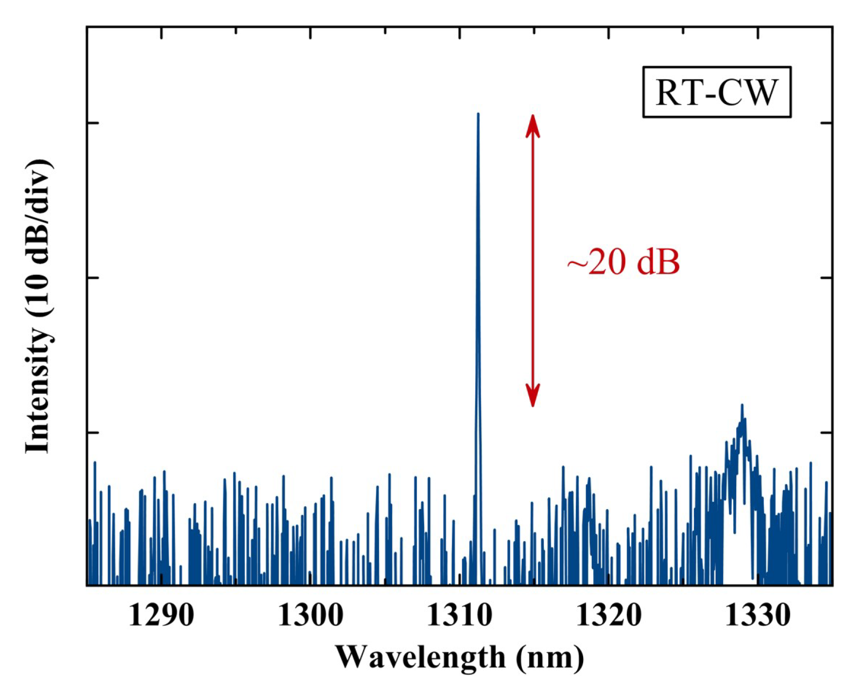
4. Experimental Demonstration of Wavelength Tuning of Cird Lasers

We reported the influence of InAs QDs on the etching process that fabricates PhC structures in an epitaxial wafer with a heterostructure (Figure 1) [31]. Air holes with minor contractions, etched on an epitaxial wafer with InAs QDs layers by using a multistep etching recipe, were obtained since we achieved a good balance between the physical and the chemical etching effects for the core layer [31]. The wavelength tuning of the CirD lasers was demonstrated using optical pumping technology [25,26]. To relax the requirements of the dry etching process, we employed a structure without a GaAs contact and upper cladding layers. The thicknesses of the GaAs core layer and the underlying AlGaAs cladding layer were 220 nm and 500 nm, respectively. The GaAs core layer contained three InAs QDs layers, and the spontaneous emission peak of QDs was designed at around 1290 nm. In addition, the entire underlying cladding layer was oxidized to AlGaOx. Typical top- and cross-sectional views of the scanning electron-microscope (SEM) pictures for the fabricated optically-driven CirD laser are shown in Figure 8a,b. Fabrication of samples and measurement set-up can be found in the references [25,26]. All experiments were conducted under RT-CW conditions.
Figure 9 shows a typical excitation power versus output intensity curve of the CirD laser (a = 345 nm, R = 2.76 a, r = 0.31 a). Threshold excitation power P t h was estimated as small as approximately 25 μW, which was almost constant even if the structure parameters of the CirD laser were modified [25]. This indicates that optically-driven CirD lasers have sufficiently high Q because the threshold hardly varies when Q is larger than 2000 (Figure 6). Note that it is quite difficult to experimentally measure Q of a laser cavity due to the co-existence of the spontaneous emission and the stimulated emission. Based on the rate equations, the linewidth of the microcavity lasers varies depending on photon density even in the same cavity which has a constant Q [32]. The linewidth varies even below the threshold. In some cases, Q is estimated from the linewidth at around the threshold, in which the gain material is almost transparent. However, this method may cause a significant error. (As shown in Figure 17 of reference [20], the linewidth just below the threshold was approxiamtely 0.05 nm, which corresponding the experimental Q of approximately 30,000. This value is as large as 10 times the calculated Q.) The threshold current of the electrically-driven CirD laser was estimated to be 4 μA [25], which agrees with the result calculated by rate equations (Figure 6). The output intensity increases with the increasing of excitation power up to about 1 mW without saturation.
Figure 10 shows the spectrum of the CirD cavity (a = 385 nm, R = 2.77 a, r = 0.29 a). The peak at 1311.25 nm corresponds to the lasing wavelength of the WGM. As be expected, we observed the single mode lasing operation. Its linewidth reached the resolution-limit of the optical spectrum analyzer: 0.07 nm, which indicates that CirD cavity may has a smaller linewidth. In addition, the side-mode suppression-ratio (SMSR) is approximately 20 dB within 50 nm wavelength range.
Figure 11 shows the dependence of the measured and calculated wavelength of the WGM on R. Although the experimentl and theoretical wavelengths are slightly different, we obtained a good match of wavelength tuning rate between experiment and simulation. The above result also confirms that the lasing mode was the WGM. The lasing wavelength was tuned over 20 nm in the R range from 2.75 a to 2.80 a. Under a high speed modulation at 50 Gbps, the linewidth of CirD laser is expected to increase to 0.3 nm due to the quick phase shift. Therefore, channel spacing of 1 nm is reasonable for the integrated CirD laser array. Then, the bandwidth capacity of 1 Tbps can be realized by WDM with 20 channles in the wavelength range of 20 nm.

5. Conclusions

We described a design of CirD lasers for inter-chip or intra-chip optical interconnects. Compact laser and PD arrays that enable WDM and WDD without a conventional optical multiplexer and a demultiplexer can be constructed by integrating several CirD cavities with one PhC line-defect waveguide. This architecture can be used to achieve an optical module with an extremely high bandwidth density for future optical interconnects. In the numerical analysis of CirD lasers, we expect Q > 2000, uniform low threshold lasing, and a modulation speed of approximately 50 Gbps within a wavelength range of 20 nm. In addition, we demonstrated single-mode lasing behaviors of CirD lasers with a linewidth <0.07 nm, a SMSR of approximately 20 dB by conducting optical pumping experiments under RT-CW conditions. The lasing wavelength of CirD lasers was modulated over 20 nm, which shows the potential of CirD lasers for WDM applications. The above results indicate that CirD lasers are a strong candidate for future optical interconnects.

Author Contributions

Conceptualization is done by Y.X., A.M., and M.K.; the mehodology is done by M.M. and A.M.; Validation is done by Y.X.; Formal analysis is done by H.Y. and Y.X.; Investigation is done by S.M., T.U., H.Y., and Y.X.; Resources are done by S.M., T.U., and Y.X.; Data curation is done by H.Y. and Y.X.; Writing-Original Draft Preparation is done by Y.X.; Writing-Review & Editing is done by M.M., H.K., A.M., and M.K.; Visualization is done by Y.X.; Supervision is done by A.M. and M.K.; Project Administration is done by Y.X.; Funding Acquisition is done by M.M., H.K., A.M., and M.K.

Funding

This research was partially supported by JSPS KAKENHI Grant Numbers JP16H04349 and JP19H02198, ULVAC, Inc., and NIPPON SHEET GLASS FOUNDATION.

Acknowledgments

The authors are grateful to Prof. M. Katayama and H. Tabata for the use of the SEM apparatus. They are also grateful to M. Tonouchi, H. Murakami, and I. Kawayama for the use of the EB lithography apparatus. This work was partially supported by Nanotechnology Platform Project (Nanotechnology Open Facilities in Osaka University) of Ministry of Education, Culture, Sports, Science and Technology, Japan [No.: F-18-OS-0026] and [No.: F-19-OS-0030].

Conflicts of Interest

The authors declare no conflict of interest.

References

  1. Young, I.A.; Mohammed, E.; Liao, J.T.; Kern, A.M.; Palermo, S.; Block, B.A.; Reshotko, M.R.; Chang, P.L. Optical I/O technology for tera-scale computing. IEEE J. Solid-State Circuits 2010, 45, 235–248. [Google Scholar] [CrossRef]
  2. Miller, S.E. Integrated optics: An introduction. Bell Syst. Tech. J. 1969, 48, 2059–2069. [Google Scholar] [CrossRef]
  3. Kim, G.; Park, J.W.; Kim, I.G.; Kim, S.; Kim, S.; Lee, J.M.; Park, G.S.; Joo, J.; Jang, K.S.; Oh, J.H.; et al. Low-voltage high-performance silicon photonic devices and photonic integrated circuits operating up to 30 Gb/s. Opt. Express 2011, 19, 26936–26947. [Google Scholar] [CrossRef] [PubMed]
  4. Zheng, X.; Luo, Y.; Lexau, J.; Liu, F.; Li, G.; Thacker, H.D.; Shubin, I.; Yao, J.; Ho, R.; Cunningham, J.E.; et al. 2-pJ/bit (on-chip) 10-Gb/s digital CMOS silicon photonic link. IEEE Photonics Technol. Lett. 2012, 24, 1260–1262. [Google Scholar] [CrossRef]
  5. Urino, Y.; Usuki, T.; Fujikata, J.; Ishizaka, M.; Yamada, K.; Horikawa, T.; Nakamura, T.; Arakawa, Y. High-density and wide-bandwidth optical interconnects with silicon optical interposers. Photonics Res. 2014, 2, A1–A7. [Google Scholar] [CrossRef]
  6. Arakawa, Y.; Nakamura, T.; Urino, Y.; Fujita, T. Silicon photonics for next generation system integration platform. IEEE Commun. Mag. 2013, 51, 72–77. [Google Scholar] [CrossRef]
  7. Fujitsu, NEDO and PETRA DevelopWorld’s Highest Transmission Density Optical Transceiver and High-Speed Energy Efficient Optical Modulator Technology. Available online: http://www.fujitsu.com/global/about/resources/news/press-releases/2017/0919-03.html (accessed on 25 March 2019).
  8. Kondow, M.; Zhang, X.; Morifuji, M. Proposal of high-density light source with 10 Pbps/cm2 for intra-chip optical-interconnections. In Proceedings of the Collaborative Collaborative Conference on 3D & Materials Research (CC3DMR 2015), Busan, Korea, 15–19 June 2015. Tu-212-1. [Google Scholar]
  9. Vlasov, Y.A.; McNab, S.J. Losses in single-mode silicon-on-insulator strip waveguides and bends. Opt. Express 2004, 12, 1622–1631. [Google Scholar] [CrossRef]
  10. Bogaerts, W.; Baets, R.; Dumon, P.; Wiaux, V.; Beckx, S.; Taillaert, D.; Luyssaert, B.; Van Campenhout, J.; Bienstman, P.; Van Thourhout, D. Nanophotonic waveguides in silicon-on-insulator fabricated with CMOS technology. J. Lightware Technol. 2005, 23, 401–412. [Google Scholar]
  11. Xu, Q.; Schmidt, B.; Pradhan, S.; Lipson, M. Micrometre-scale silicon electro-optic modulator. Nature 2005, 435, 325. [Google Scholar] [CrossRef]
  12. Huang, Z.; Carey, J.E.; Liu, M.; Guo, X.; Mazur, E.; Campbell, J.C. Microstructured silicon photodetector. Appl. Phys. Lett. 2006, 89, 033506. [Google Scholar] [CrossRef]
  13. Liu, A.Y.; Bowers, J. Photonic Integration with Epitaxial III–V on Silicon. IEEE J. Sel. Top. Quantum Electron. 2018, 24, 1–12. [Google Scholar] [CrossRef]
  14. Yablonovitch, E. Inhibited spontaneous emission in solid-state physics and electronics. Phys. Rev. Lett. 1987, 58, 2059. [Google Scholar] [CrossRef] [PubMed]
  15. Akahane, Y.; Asano, T.; Song, B.S.; Noda, S. High-Q photonic nanocavity in a two-dimensional photonic crystal. Nature 2003, 425, 944. [Google Scholar] [CrossRef] [PubMed]
  16. O’Brien, J.; Kuang, W.; Cao, J.-R.; Shih, M.-H.; Lee, P.-T.; Bagheri, M.; Mock, A.; Marshall, W.K. Photonic crystal microcavity lasers. J. Phys. D Appl. Phys. 2007, 40, 2671. [Google Scholar] [CrossRef]
  17. Nomura, M.; Kumagai, N.; Iwamoto, S.; Ota, Y.; Arakawa, Y. Photonic crystal nanocavity laser with a single quantum dot gain. Opt. Express 2009, 17, 15975–15982. [Google Scholar] [CrossRef] [PubMed]
  18. Takeda, K.; Sato, T.; Shinya, A.; Nozaki, K.; Kobayashi, W.; Taniyama, H.; Notomi, M.; Hasebe, K.; Kakitsuka, T.; Matsuo, S. Few-fJ/bit data transmissions using directly modulated lambda-scale embedded active region photonic-crystal lasers. Nat. Photonics 2013, 7, 569. [Google Scholar] [CrossRef]
  19. Kuramochi, E.; Nozaki, K.; Shinya, A.; Takeda, K.; Sato, T.; Matsuo, S.; Taniyama, H.; Sumikura, H.; Notomi, M. Large-scale integration of wavelength-addressable all-optical memories on a photonic crystal chip. Nat. Photonics 2014, 8, 474. [Google Scholar] [CrossRef]
  20. Matsuo, S.; Sato, T.; Takeda, K.; Shinya, A.; Nozaki, K.; Kuramochi, E.; Taniyama, H.; Notomi, M.; Fujii, T.; Hasebe, K.; et al. Photonic crystal lasers using wavelength-scale embedded active region. J. Phys. D Appl. Phys. 2013, 47, 023001. [Google Scholar] [CrossRef]
  21. Nozaki, K.; Matsuo, S.; Takeda, K.; Fujii, T.; Ono, M.; Shakoor, A.; Kuramochi, E.; Notomi, M. Sub-fF-capacitance photonic-crystal photodetector towards fJ/bit on-chip receiver. IEICE Trans. Electron. 2017, 100, 750–758. [Google Scholar] [CrossRef]
  22. Nishi, H.; Takeda, K.; Fujii, T.; Kuramochi, E.; Shinya, A.; Notomi, M.; Tsuchizawa, T.; Kakitsuka, T.; Matsuo, S. Low-Operating Energy Heterogeneously Integrated Photonic-Crystal Laser on Si Waveguide. In Proceedings of the IEEE International Semiconductor Laser Conference (ISLC), Santa Fe, NM, USA, 16–19 September 2018; pp. 1–2. [Google Scholar]
  23. Fujii, T.; Takeda, K.; Diamantopoulos, N.P.; Kanno, E.; Hasebe, K.; Nishi, H.; Nakao, R.; Kakitsuka, T.; Matsuo, S. Heterogeneously integrated membrane lasers on Si substrate for low operating energy optical links. IEEE J. Sel. Top. Quantum Electron. 2018, 24, 1–8. [Google Scholar] [CrossRef]
  24. Morifuji, M.; Nakaya, Y.; Mitamura, T.; Kondow, M. Novel design of current driven photonic crystal laser diode. IEEE Photonics Technol. Lett. 2009, 21, 513–515. [Google Scholar] [CrossRef]
  25. Zhang, X.; Hino, T.; Kasamatsu, S.; Suga, S.; He, E.; Xiong, Y.; Morifuji, M.; Kajii, H.; Maruta, A.; Kondow, M. 1.3 μm lasing of circular defect cavity photonic crystal laser with an AlOx cladding layer. IEICE Electron. Express 2017, 14, 20170664. [Google Scholar] [CrossRef]
  26. Xiong, Y.; Umeda, T.; Zhang, X.; Morifuji, M.; Kajii, H.; Maruta, A.; Kondow, M. Photonic Crystal Circular-Defect Microcavity Laser Designed for Wavelength Division Multiplexing. IEEE J. Sel. Top. Quantum Electron. 2018, 24, 1–7. [Google Scholar] [CrossRef]
  27. Faraon, A.; Waks, E.; Englund, D.; Fushman, I.; Vučković, J. Efficient photonic crystal cavity-waveguide couplers. Appl. Phys. Lett. 2007, 90, 073102. [Google Scholar] [CrossRef]
  28. Network Source of Refractive Indexes of the Materials Used in the Model. Available online: https://refractiveindex.info/ (accessed on 25 March 2019).
  29. Nozaki, K.; Baba, T. Carrier and photon analyses of photonic microlasers by two-dimensional rate equations. IEEE J. Sel. Areas Commun. 2005, 23, 1411–1417. [Google Scholar] [CrossRef]
  30. Bowers, J.; Hemenway, B.; Gnauck, A.; Wilt, D. High-speed InGaAsP constricted-mesa lasers. IEEE J. Quantum Electron. 1986, 22, 833–844. [Google Scholar] [CrossRef]
  31. Zhang, X.; Takeuchi, K.; Cong, X.; Xiong, Y.; Morifuji, M.; Maruta, A.; Kajii, H.; Kondow, M. Dry etching of deep air holes in GaAs/AlGaAs-based epi-wafer having InAs quantum dots for fabrication of photonic crystal laser. Jpn. J. Appl. Phys. 2017, 56, 126501. [Google Scholar] [CrossRef]
  32. Björk, G.; Karlsson, A.; Yamamoto, Y. On the linewidth of microcavity lasers. Appl. Phys. Lett. 1992, 60, 304–306. [Google Scholar] [CrossRef]
Figure 1. Schematic of electrically-driven CirD laser.
Photonics 06 00054 g001
Figure 2. Magnetic field intensity ( | H z | ) distribution of Circular Defect (CirD) lasers. Circles represent air holes.
Photonics 06 00054 g002
Figure 3. (a) Schematic of CirD laser array architecture enabled wavelength division multiplexing (WDM). (b) Schematic of CirD laser array in which each cavity is isolated by current blocking trench. 5 μm × 5 μm area outside of cavity is used as the bonding pad.
Photonics 06 00054 g003
Figure 4. (a) Schematic of monolithic integrated optical module combined with wavelength division multiplexing and demultiplexing functions. (b) Schematic of flip-chip boding of integrated optical module to silicon substrate.
Photonics 06 00054 g004
Figure 5. Resonant wavelength ( λ ) and quality factor ( Q s ) of CirD cavity dependent on radius of cavity (R).
Photonics 06 00054 g005
Figure 6. Lasing threshold ( I t h ) versus Q for CirD lasers.
Photonics 06 00054 g006
Figure 7. Relaxation oscillation frequency ( f r ) as a function of injection current.
Photonics 06 00054 g007
Figure 8. (a) Top-view and (b) cross-sectional view of SEM pictures for fabricated optically-driven CirD laser.
Photonics 06 00054 g008
Figure 9. Output intensity as a function of excitation power for optically-driven CirD laser.
Photonics 06 00054 g009
Figure 10. Lasing spectrum at pumping power of approximately 800 μW. (reprinted with permission from reference [26], IEEE).
Photonics 06 00054 g010
Figure 11. Measured and theoretically estimated lasing wavelengths of WGM as a function of R. Fabricated a and r were kept approximately constant at 385 nm and 0.29 a. (reprinted with permission from reference [26], IEEE).
Photonics 06 00054 g011
Table 1. Values of parameters used to construct 3D model of CirD lasers.
ParametersValue
Thickness of GaAs contact layer180 nm
Thickness of AlGaAs/AlGaOx cladding layers500 nm
Thickness of GaAs core layer220 nm
Lattice constant a360 nm
Radius of air holes0.3 a
AlGaOx width0.8 a
Refractive index of GaAs3.400
Refractive index of AlGaAs2.924
Refractive index of AlOx1.761
Refractive index of air1.000
Table 2. Values of parameters for rate equation analysis.
SymbolParametersValue
Γ z Confinement factor at the vertical direction0.07
g 0 Gain coefficient10 5 m 1
N 0 Transparent carrier density10 23 m 3
DCarrier diffusion constant (out side of the air holes)2 × 10 3 m2/s
τ c Carrier lifetime1 ns
v g Group velocity8.82 × 10 7 m/s
VCarrier injection area volume2.23 × 10 20 m 3
A m Effective modal area3.52 × 10 13 m2

