Letter

The Role of Electron Transfer in the Nonlinear Response of Ge2Sb2Te5-Mediated Plasmonic Dimers

by
Burak Gerislioglu
1 and
Arash Ahmadivand
2,*
1
Department of Physics and Astronomy, Rice University, 6100 Main St, Houston, TX 77005, USA
2
Department of Electrical and Computer Engineering, Rice University, 6100 Main St, Houston, TX 77005, USA
*
Author to whom correspondence should be addressed.
Photonics 2019, 6(2), 52; https://doi.org/10.3390/photonics6020052
Submission received: 29 April 2019 / Revised: 13 May 2019 / Accepted: 14 May 2019 / Published: 16 May 2019

Abstract

:
Here, we study the possibility of exquisitely selective harmonic generation based on the concept of charge transfer plasmons (CTPs) in bridged nanoparticle assemblies. By choosing plasmonic dimer nanoantenna, as a fundamental member of the nanocluster family, and bridging the capacitive gap space between the proximal nanoparticles with an optothermally controllable substance, we judiciously showed that variations in the generation of third harmonic light in the visible regime can be possible by considering distinct states of the functional bridge. To this end, the conductive connection between the nanoparticles is mediated with Ge2Sb2Te5 (GST) with inherently opposite optical and electrical properties below (dielectric, amorphous state) and above 477 °C (conductive, crystalline state). This helped to actively control the transition of charges across the bridge and thereby control the excitation of CTP resonances and provide a switching feature between dipolar and CTP modes. This versatile approach also allowed for production of the intended harmonic signal at different wavelengths depending on the conductivity of the interparticle nanojunction.

1. Introduction

Nonlinear plasmonics is one of the fundamental counterparts of optics and photonics, with a wide range of fascinating applications in the development of integrated nanolasers, advanced light sources, and next-generation subwavelength devices [1,2,3]. An intense localization of optically driven hot electrons in plasmonic structures, at the associated resonant frequency, substantially enhances the nonlinear optical effects, leading to an active control over incident light in the subwavelength regime [4]. As a conventional nonlinear phenomenon, harmonic generation has been observed and reported in gas atoms, such as argon (Ar) and xenon (Xe), because of multiphoton ionization [5]. To date, the generation of high-order harmonics has been successfully achieved using various systems, such as nanophotonic and plasmonic structures [4,6,7]. Here, the major idea is based on the conversion of fundamental incident beam frequency into the intense harmonics by using nanoscale solids with large field-induced susceptibilities (χ(2) or χ(3)) [1,2,3,4,8], and one of the successful and promising approaches for the harmonic generation is the use of resonant nanostructures, including both plasmonic and high-index all-dielectric systems.
For instance, Fano-resonant nanodevices are one of the most popular design modalities to induce nonlinear features. Taking advantage of strong hotspots and near-field coupling in Fano-resonant systems, highly intense nonlinear responses have already been achieved [9,10]. Although there have been significant achievements in the nonlinear plasmonics, these systems still suffer from poor selectivity. In other words, the generation of both odd and even harmonics using a single integrated system would help to develop miniature lasers and multifunctional nonlinear metadevices. To address this shortcoming, graphene monolayers with the ability to tune the induced plasmonic response have been proposed for extreme nonlinear photonics using Kerr nonlinearity [11,12]. However, graphene-based nanostructures are not fully functional, owing to complex and expensive fabrication techniques, and lack of mechanical flexibility [13,14].
Recently, a new spectral feature has been introduced, known as charge transfer plasmons (CTPs), utilizing plasmonic nanostructures [15,16,17,18,19,20,21,22,23,24] and nanoparticles with conductive junctions [25,26,27,28]. In both cases, a direct transition of charges across the conductive nanoparticles acts as a fundamental component for the excitation of CTPs. So far, several approaches have been provided to increase the inherent and limited tunability of CTPs, such as using phase-change materials (PCMs), (i.e., Ge2Sb2Te5 (GST), VO2) [27] and graphene monolayers [28] to adjust the CTP feature. Tunable CTPs have been recently employed for developing ultrafast telecommunication devices, such as switches and metamodulators [25,27].
In this letter, we report the first study of the use of optothermally tunable CTP-resonant nanodimers for the selective generation of a third harmonic signal. In this regard, we utilized a simple nanodimer composed of two nanodisks connected to each other with a metallodielectric junction consisting of metallic and PCM (here, GST) blocks. Particularly, GST possesses significant characteristics above and below 477 °C [29,30]. Such a unique feature allows for modifying the shuttling of charges across the bridge and, thus, tunes the generated nonlinear response towards the targeted harmonic. Previously, we have employed this exquisite feature for plasmonic switching application at a telecommunication band [27]. We demonstrated that applying either optical or external heat stimuli facilitates an interplay between the opposite phases of the GST bridge, and gives rise to quick switching between all-dielectric and conductive phases. From the nonlinear application perspective, when the GST-mediated nanobridge is in the dielectric regime, the capacitive coupling is dominant, and the dipolar extreme appears at λ~1880 nm. Conversely, when the GST part of the bridge turns into the crystalline state, the bridge acts as a nearly metallic junction and forms a CTP peak around λ ~ 2150 nm. Our findings indicate that this switching mechanism can be used towards adjustable harmonic generation depending on the phase of optothermally controllable substance in nanoplasmonic structures.

2. Results and Discussion

Figure 1a demonstrates a general view of the proposed metallodielectric dimer (not to scale). The geometric parameters are specified in Figure 1b. The following dimensions are utilized for the platform: width/length/depth (W/L/D) = 50 nm, 30 nm, and 200 nm, respectively. The total length of the compositional bridge is fixed to 200 nm. It is assumed that the metallodielectric dimer is deposited on a glass (SiO2) substrate with Palik permittivity constants [31]. Here, the nanodisks are gold (Au) with Johnson and Christy constants [32]. The complex permittivity values for GST at both phases (see Figure 1c,d) were taken from the experimental results reported by Shportko et al. [33]. In our electromagnetic analyses, we presumed that the GST and Au parts of the nanobridge are perfectly matched, and the thickness is homogenous and fixed to t = 45 nm.
Here, we focus on extracting the spectral response of the metallodielectric dimer under x-polarized (TM) beam illumination for three different states of the bridge: dielectric (a-GST), conductive (c-GST), and fully metallic (Au) regimes. The normalized extinction spectra of the proposed platform are exhibited in Figure 2a. For the full Au junction, the structure acts as a classical CTP-resonant system, and a pronounced CTP mode is formed around λ ~ 2400 nm due to free transition of the charges across the conductive path. The excited CTP peak for the fully metallic regime is not tunable and morphological variations must be applied to tune the spectral feature. By introducing a small section of GST at the center of Au nanobridge, an efficient modification of the plasmonic response of the nanoassembly would be possible. To this end, initially, we assumed that GST is in the amorphous state and acts similar to a dielectric spacer (i.e., air). This results in the formation of a classical dipole at λ~1880 nm owing to strong capacitive coupling between the proximal nanostructures. Switching the state of GST to crystalline regime by applying optical stimuli, we facilitate the transition of charges instead of coupling. The low electrical resistivity feature of the c-GST phase (~10−3 Ω.cm) leads to the formation of a CTP peak around λ ~ 2150 nm. It should be noted that a shoulder appeared in all analyzed regimes around λ ~ 650 nm (p1) correlating with the dipolar moment. The |E|-field maps across the nanoassembly are plotted in Figure 2b,c, using both FDTD and FEM tools. Obviously, by moving from a-GST (Figure 2b,c (i)) to c-GST, Figure 2b,c (ii)) regime) the capacitive coupling turns to the direct charge transfer and therefore, dipolar moment is transformed to the CTP mode. Relatively, for the dimer with the fully metallic junction, the induced charges can easily travel along the junction and concentrate at the outermost nanodisks (Figure 2b,c (iii)).
Next, we study the nonlinear response of the proposed functional nanodimer for selective generation of the third harmonic signal. To this end, we use the obtained fundamental resonance wavelength in linear electromagnetic simulations for both regimes of the bridge, a-GST and c-GST, as a source wavelength (see Numerical Analysis). As shown in Figure 3a, in the a-GST limit and for the incidence with the fundamental wavelength of λ~1880 nm (ω), we observed the formation of third harmonic signal at λ~628 nm (3ω). On the other hand, for the metallodielectric dimer with c-GST nanobridge, the third harmonic signal is generated at λ~2150 nm (ω) in comparison to its primary wavelength λ~717 nm (3ω) (see Figure 3b). It is important to note that there is an insignificant deviation around 1–2 nm for both cases, since we neglected the effect of the third harmonic susceptibility dispersion.
The geometric variations in the structural parameters of the dimer reveal strong dependency on the generated harmonic signal. Figure 4 and Figure 5 illustrate the variations in the length (L) and width (W) of the bridge, respectively, and the corresponding intensity profile for each condition. These results validate the highest harmonic signal intensity of λ~11 for the following geometries: W/L/t = 80/30/45 nm. Technically, when the length of a-GST unit is increased from 30 nm to 50, 80, and 100 nm, the wavelength of the harmonic dramatically blue-shifts up to 469.5 nm, while the intensity decreases in contrast to the starting case (see Figure 4a (i–iii)). Similar to the a-GST harmonic generation analysis, when the length of the c-GST section is increased from 30 nm to 50, 80, and 100 nm, the wavelength of the induced harmonic blue-shifts up to 617.7 nm. It is obvious from Figure 4b (i,ii) that change in length from 50 to 80 nm reduces the signal intensity, whereas further modification from 80 to 100 nm increases the harmonic intensity in Figure 4b (ii,iii) (see Table 1). For the bridge width variations from 60 to 80 nm, we obtained a substantial increment in the intensity as well as a slight blue-shift in the position of the harmonic (see Figure 5a (ii,iii)). Interestingly, in Figure 5a (i), when the bridge width is shrunk from 50 to 40 nm, the induced harmonic resonance is red shifted to 630.6 nm, as its intensity is increased up to 2.25. When the a-GST is converted into the c-GST, increasing the width of the GST regime from 60 to 80 nm leads to significant decays in the intensity and blue-shifts the location of the excited harmonic to 678.3 nm. Likewise, to the a-GST limit, once the bridge width is reduced from 50 to 40 nm, the harmonic is red-shifted to 735.6 nm, while the signal strength is enhanced to 1.75 (see Figure 5b and Table 2).

3. Numerical Analysis

The corresponding 3D electromagnetic simulations of the proposed platform were performed using finite-difference time-domain (FDTD, Lumerical) and finite element methods (FEM, COMSOL Multiphysics). The boundaries of the simulation region were surrounded with 128 layers of absorptive perfectly matched layers (PMLs), the spatial gridding cell sizes were set to 0.5 nm in all axes, and periodic boundary conditions were applied to compose a plasmonic metasurface. To satisfy the Courant stability factor (~0.99), we set the simulation time step to 0.0199 fs [34]. The incident beam radiation was a broadband plane wave (400–1600 nm), with the irradiation power of P0 = 3.2 µW, beam fluence of 60 Jm−2, pulse length of 250 fs, and a repetition rate of 10 KHz. Additionally, we utilized a light source with a duration of 0.9 ns and the irradiation power of 5.5 mW to provide the required thermal energy for the amorphization process. The nonlinear response of the system was modeled using Maxwell’s equations and introducing Au as a nonlinear material with a superb susceptibility value (χ(3)) [35] in FDTD. To this end, the following equation was solved: P(3) = ε0χ(3)Ej(E·E), where P is the nonlinear polarization, ε0 is the permittivity of vacuum, and Ej is the electric field (E) component in all there axis. Ultimately, for a fixed beam power, the corresponding conversion efficiency values (P(3ω)/P(ω)) for both states was defined as ηa-GST and ηc-GST, and they were 0.0015% and 0.0004%, respectively.

4. Conclusions

In this work, we have demonstrated that an optothermally controllable plasmonic platform for quick, all-optical, and functional frequency generation in the visible band. Based on the use of the unique electrical and optical features of GST substance, we have recognized the excitation of the third harmonic signal at different wavelengths depending on the phase of the GST, without requiring any geometrical changes. To this end, we have reported the first numerical realization of the harmonic generation using the interplay between the dipolar and CTP modes. This approach clearly shows that how such a practical and fundamental platform can be utilized as an active system for the harmonic generation. We believe that our outcomes show the potential of this method for the next generation of practical nonlinear optical devices.

Author Contributions

Conceptualization, B.G. and A.A.; Formal analysis, B.G. and A.A.; Writing, review and editing, B.G. and A.A.; Project administration, B.G. and A.A.

Funding

This research received no external funding.

Conflicts of Interest

The authors declare no conflict of interest.

References

  1. Suh, J.Y.; Kim, C.H.; Zhou, W.; Huntington, M.D.; Co, D.T.; Wasielewski, M.R.; Odom, T.W. Plasmonic bowtie nanolaser arrays. Nano Lett. 2012, 12, 5769–5774. [Google Scholar] [CrossRef] [PubMed]
  2. Ropers, C.; Neacsu, C.C.; Elsaesser, T.; Albrecht, M.; Raschke, M.B.; Lienau, C. Grating-coupling of surface plasmons onto metallic tips: A nanoconfined light source. Nano Lett. 2007, 7, 2784–2788. [Google Scholar] [CrossRef]
  3. Neira, A.D.; Olivier, N.; Nasir, M.E.; Dickson, W.; Wurtz, G.A.; Zayats, A.V. Eliminating material constraints for nonlinearity with plasmonic metamaterials. Nat. Commun. 2015, 6, 7757. [Google Scholar] [CrossRef] [PubMed] [Green Version]
  4. Kauranen, M.; Zayats, A.V. Nonlinear plasmonics. Nat. Photon. 2012, 6, 737–748. [Google Scholar] [CrossRef]
  5. Ferray, M.; L’Huillier, A.; Li, X.F.; Lompre, L.A.; Mainfray, G.; Manus, C. Multiple-Harmonic Conversion of 1064 nm Radiation in Rare Gases. J. Phys. B At. Mol. Opt. Phys. 1988, 21, L31. [Google Scholar] [CrossRef]
  6. Gerislioglu, B.; Ahmadivand, A.; Pala, N. Hybridized plasmons in graphene nanorings for extreme nonlinear optics. Opt. Mater. 2017, 73, 729–735. [Google Scholar] [CrossRef]
  7. Ahmadivand, A.; Gerislioglu, B.; Pala, N. Optothermally controllable multiple high-order harmonics generation by Ge2Sb2Te5-mediated Fano clusters. Opt. Mater. 2018, 84, 301–306. [Google Scholar] [CrossRef]
  8. Cai, W.; Vasudev, A.P.; Brongersma, M.L. Electrically controlled nonlinear generation of light with plasmonics. Science 2011, 333, 1720–1723. [Google Scholar] [CrossRef]
  9. Thyagarajan, K.; Butet, J.; Martin, O.J. Augmenting second harmonic generation using Fano resonances in plasmonic systems. Nano Lett. 2013, 13, 1847–1851. [Google Scholar] [CrossRef]
  10. Shcherbakov, M.R.; Neshev, D.N.; Hopkins, B.; Shorokhov, A.S.; Staude, I.; Melik-Gaykazyan, E.V.; Decker, M.; Ezhov, A.A.; Miroshnichenko, A.E.; Brener, I.; et al. Enhanced third-harmonic generation in silicon nanoparticles driven by magnetic response. Nano Lett. 2014, 14, 6488–6492. [Google Scholar] [CrossRef]
  11. Cox, J.D.; Marini, A.; de Abajo, F.J.G. Plasmon-assisted high-harmonic generation in graphene. Nat. Commun. 2017, 8, 14380. [Google Scholar] [CrossRef] [Green Version]
  12. Hong, S.-Y.; Dadap, J.I.; Petrone, N.; Yeh, P.-C.; Hone, J.; Osgood, R.M., Jr. Optical third-harmonic generation in graphene. Phys. Rev. X 2013, 3, 021014. [Google Scholar] [CrossRef]
  13. Ahmadivand, A.; Gerislioglu, B.; Noe, G.T.; Mishra, Y.K. Gated graphene enabled tunable charge-current configurations in hybrid plasmonic metamaterials. ACS Appl. Electron. Mater. 2019. [Google Scholar] [CrossRef]
  14. Wang, X.; Chen, C.; Pan, L.; Wang, J. A graphene-based Fabry-Perot spectrometer in mid-infrared region. Sci. Rep. 2016, 6, 32616. [Google Scholar] [CrossRef]
  15. Romero, I.; Aizpurua, J.; Bryant, G.W.; de Abajo, F.J.G. Plasmons in nearly touching metallic nanoparticles: Singular response in the limit of touching dimers. Opt. Express 2016, 14, 9988–9999. [Google Scholar] [CrossRef]
  16. Ahmadivand, A.; Gerislioglu, B.; Ramezani, Z. Gated graphene island-enabled tunable charge transfer plasmon terahertz metamodulator. Nanoscale 2019, 11, 8091–8095. [Google Scholar] [CrossRef] [PubMed]
  17. Gerislioglu, B.; Ahmadivand, A.; Pala, N. Optothermally controlled charge transfer plasmons in Au-Ge2Sb2Te5 core-shell dimers. Plasmonics 2018, 13, 1921–1928. [Google Scholar] [CrossRef]
  18. Perez-Gonzalez, O.; Zabala, N.; Borisov, A.G.; Halas, N.J.; Nordlander, P.; Aizpurua, J. Optical spectroscopy of conductive junctions in plasmonic cavities. Nano Lett. 2010, 10, 3090–3095. [Google Scholar] [CrossRef]
  19. Perez-Gonzalez, O.; Zabala, N.; Aizpurua, J. Optical characterization of charge transfer and bonding dimer plasmons in linked interparticle gaps. New J. Phys. 2011, 13, 083013. [Google Scholar] [CrossRef] [Green Version]
  20. Savage, K.J.; Hawkeye, M.M.; Esteban, R.; Borisov, A.G.; Aizpurua, J.; Baumberg, J.J. Revealing the quantum regime in tunneling plasmons. Nature 2012, 491, 574–577. [Google Scholar] [CrossRef] [PubMed]
  21. Wang, Y.; Li, Z.; Zhao, K.; Sobhani, A.; Zhu, X.; Fang, Z.; Halas, J.N. Substrate-mediated charge transfer plasmons in simple and complex nanoparticle clusters. Nanoscale 2013, 5, 9897–9901. [Google Scholar] [CrossRef] [PubMed]
  22. Tserkezis, C.; Herrmann, L.O.; Valev, V.K.; Baumberg, J.J.; Aizpurua, J. Optical response of threaded chain plasmons: From capacitive chains to continuous nanorods. Opt. Express 2014, 22, 23851–23860. [Google Scholar] [CrossRef]
  23. Tan, S.F.; Wu, L.; Yang, J.K.W.; Bai, P.; Bosman, M.; Nijhuis, C.A. Quantum plasmon resonances controlled by molecular tunnel junctions. Science 2014, 343, 1496–1499. [Google Scholar] [CrossRef]
  24. Georgiou, G.; Tserkezis, C.; Schaafsma, M.C.; Aizpurua, J.; Rivas, J.G. Active loaded plasmonic antennas at terahertz frequencies: Optical control of their capacitive-inductive coupling. Phys. Rev. B 2015, 91, 125443. [Google Scholar] [CrossRef]
  25. Gerislioglu, B.; Ahmadivand, A.; Pala, N. Functional quadrumer clusters for switching between Fano and charge transfer plasmons. IEEE Photon. Technol. Lett. 2017, 29, 2226–2229. [Google Scholar] [CrossRef]
  26. Ahmadivand, A.; Gerislioglu, B.; Pala, N. Azimuthally and radially excited charge transfer plasmon and Fano lineshapes in conductive sublayer-mediated nanoassemblies. J. Opt. Am. A 2017, 34, 2052–2056. [Google Scholar] [CrossRef]
  27. Ahmadivand, A.; Gerislioglu, B.; Sinha, R.; Karabiyik, M.; Pala, N. Optical switching using transition from dipolar to charge transfer plasmon modes in Ge2Sb2Te5 bridged metallodielectric dimers. Sci. Rep. 2017, 7, 42807. [Google Scholar] [CrossRef]
  28. Ahmadivand, A.; Gerislioglu, B.; Pala, N. Graphene optical switch based on charge transfer plasmons. Phys. Status Solidi-R 2017, 11, 1700285. [Google Scholar] [CrossRef]
  29. Kim, J.-H. Correlation between microstructure and optical properties of Ge2Sb2Te5 thin films. J. Appl. Phys. 1999, 86, 6770–6772. [Google Scholar] [CrossRef]
  30. Bakan, G.; Gerislioglu, B.; Dirisaglik, F.; Jurado, Z.; Sullivan, L.; Dana, A.; Lam, C.; Gokirmak, A.; Silva, H. Extracting the temperature distribution on a phase-change memory cell during crystallization. J. Appl. Phys. 2016, 120, 164504. [Google Scholar] [CrossRef] [Green Version]
  31. Palik, E.D. Handbook of Optical Constants of Solids; Academic Press: Orlando, FL, USA, 1985. [Google Scholar]
  32. Jackson, J.D. Classical Electrodynamics; Wiley: Hoboken, NJ, USA, 1999. [Google Scholar]
  33. Shportko, K.; Kremers, S.; Woda, M.; Lencer, D.; Robertson, J.; Wuttig, M. Resonant bonding in crystalline phase-change materials. Nat. Mater. 2008, 7, 653–658. [Google Scholar] [CrossRef] [PubMed]
  34. Zheng, F.; Chen, Z. Numerical dispersion analysis of the unconditionally stable 3-D ADI-FDTD method. IEEE Trans. Microwave Theory Tech. 2001, 49, 1006–1009. [Google Scholar] [CrossRef] [Green Version]
  35. Lassiter, J.B.; Chen, X.; Liu, X.; Ciracì, C.; Hoang, T.B.; Larouche, S.; Oh, S.; Mikkelsen, M.H.; Smith, D.R. Third-harmonic generation enhancement by film-coupled plasmonic stripe resonators. ACS Photonics 2014, 1, 1212–1217. [Google Scholar] [CrossRef]
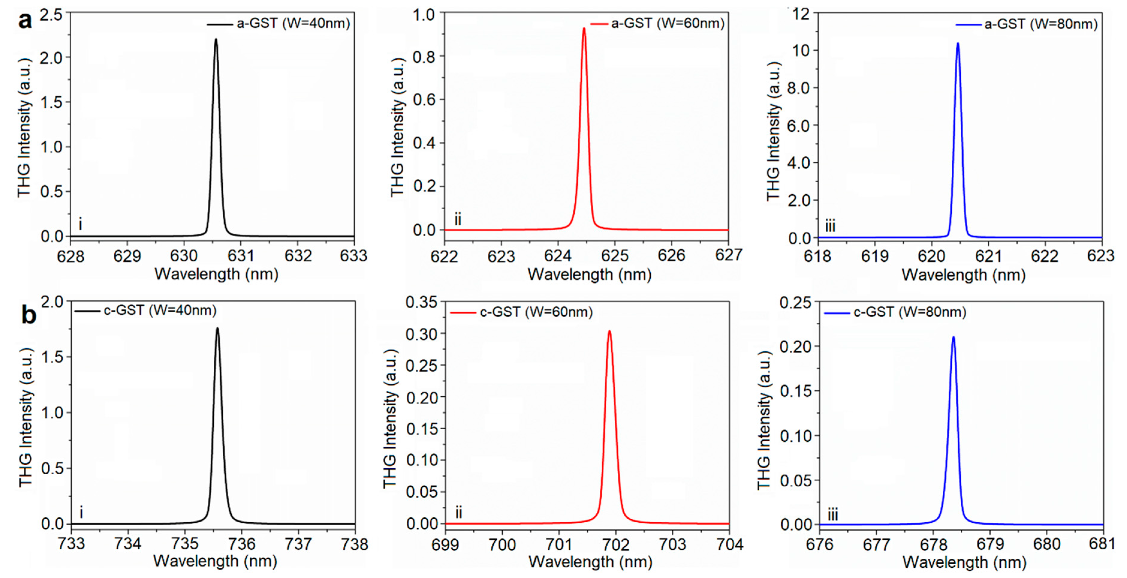
Figure 1. (a) General and (b) top-view schematics of a single unit cell. (c) ε1 and ε2 values for both GST phases (taken from Ref. 33).
Photonics 06 00052 g001
Figure 2. (a) Simulated extinction spectra of the plasmonic dimer platform for the junction with full Au, a- and c-GST sections. (b) The corresponding 2D |E|-field maps of the proposed system (FDTD): (i) dipolar mode (p2) at λ~1880 nm for a-GST, (ii) CTP mode (p3) at λ~2150 nm for c-GST, and CTP mode (p4) at λ~2400 nm for full Au. (c) The associated 2D surface charge density maps of the design (FEM): (i) dipolar mode (a-GST), (ii) CTP mode (c-GST), and CTP mode (full Au).
Photonics 06 00052 g002
Figure 3. The third harmonic emission spectrum of (a) a-GST and (b) c-GST based metadevice.
Photonics 06 00052 g003
Figure 4. The third harmonic emission spectrum of (a) a-GST and (b) c-GST cases for the variations in L: (i) 50 nm, (ii) 80 nm, and (iii) 100 nm.
Photonics 06 00052 g004
Figure 5. The third harmonic emission spectrum of (a) a-GST and (b) c-GST conditions for the variations in W: (i) 40 nm, (ii) 60 nm, and (iii) 80 nm.
Photonics 06 00052 g005
Table 1. Effect of the geometric variations in the structural parameters on the generated third harmonic signal intensity and position for a-GST.
Length (L)Width (W)
50 nm80 nm100 nm40 nm60 nm80 nm
Third harmonic signal intensity0.06250.3470.592.230.9210.8
Third harmonic signal position587.4 nm520 nm469.5 nm630.55 nm624.4 nm620.4 nm
Table 2. Effect of the geometric variations in the structural parameters on the generated third harmonic signal intensity and position for c-GST.
Length (L)Width (W)
50 nm80 nm100 nm40 nm60 nm80 nm
Third harmonic signal intensity0.550.140.831.750.30.22
Third harmonic signal position685.1 nm637.9 nm617.6 nm735.6 nm701.9 nm678.4 nm

