Influence of a Surface Finishing Method on Light Collection Behaviour of PWO Scintillator Crystals


Abstract
:1. Introduction
2. Materials and Methods
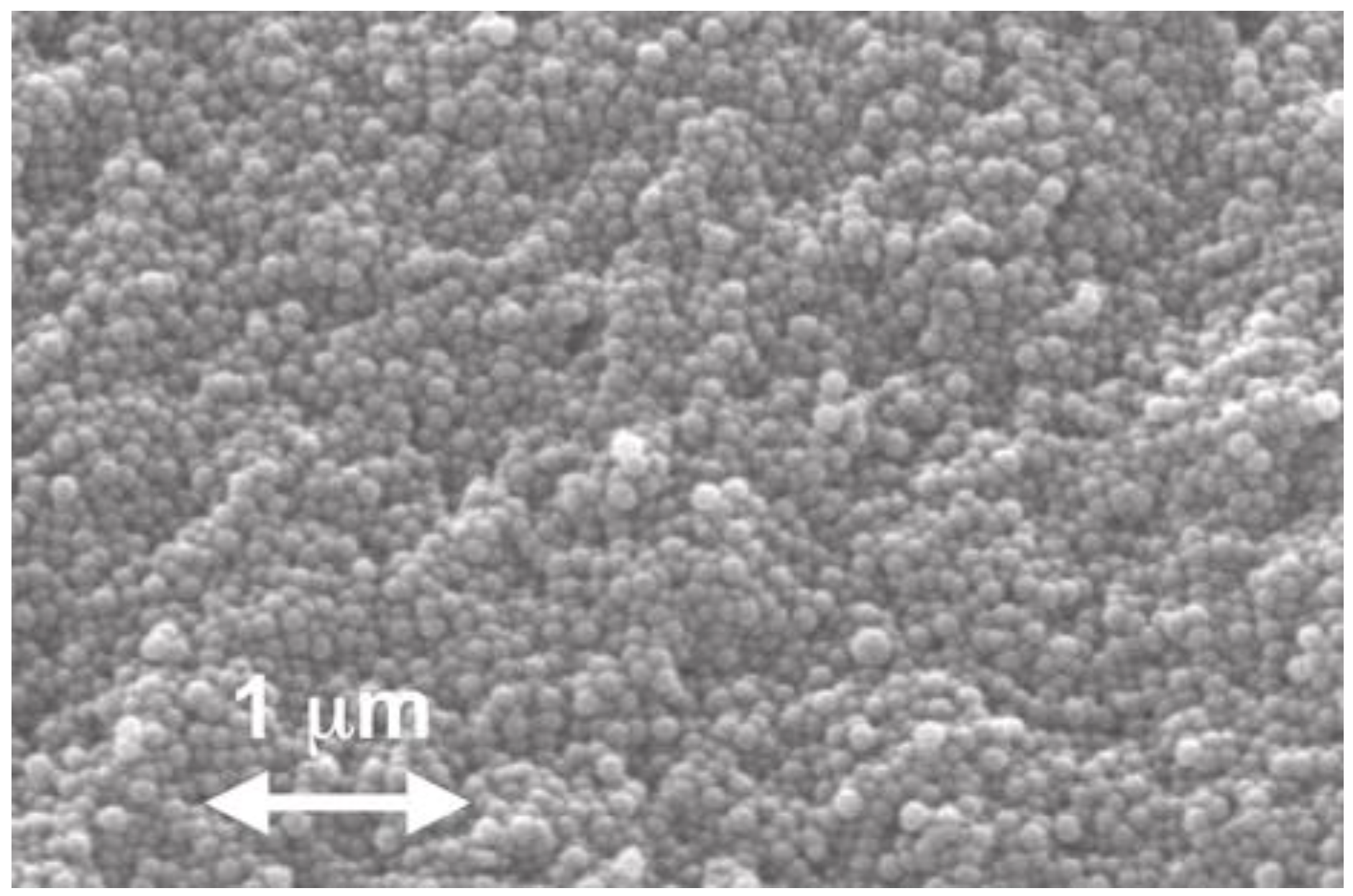
2.1. Mechanical Diamond Polishing (MDP)
2.2. Chemical Mechanical Polishing (CMP)
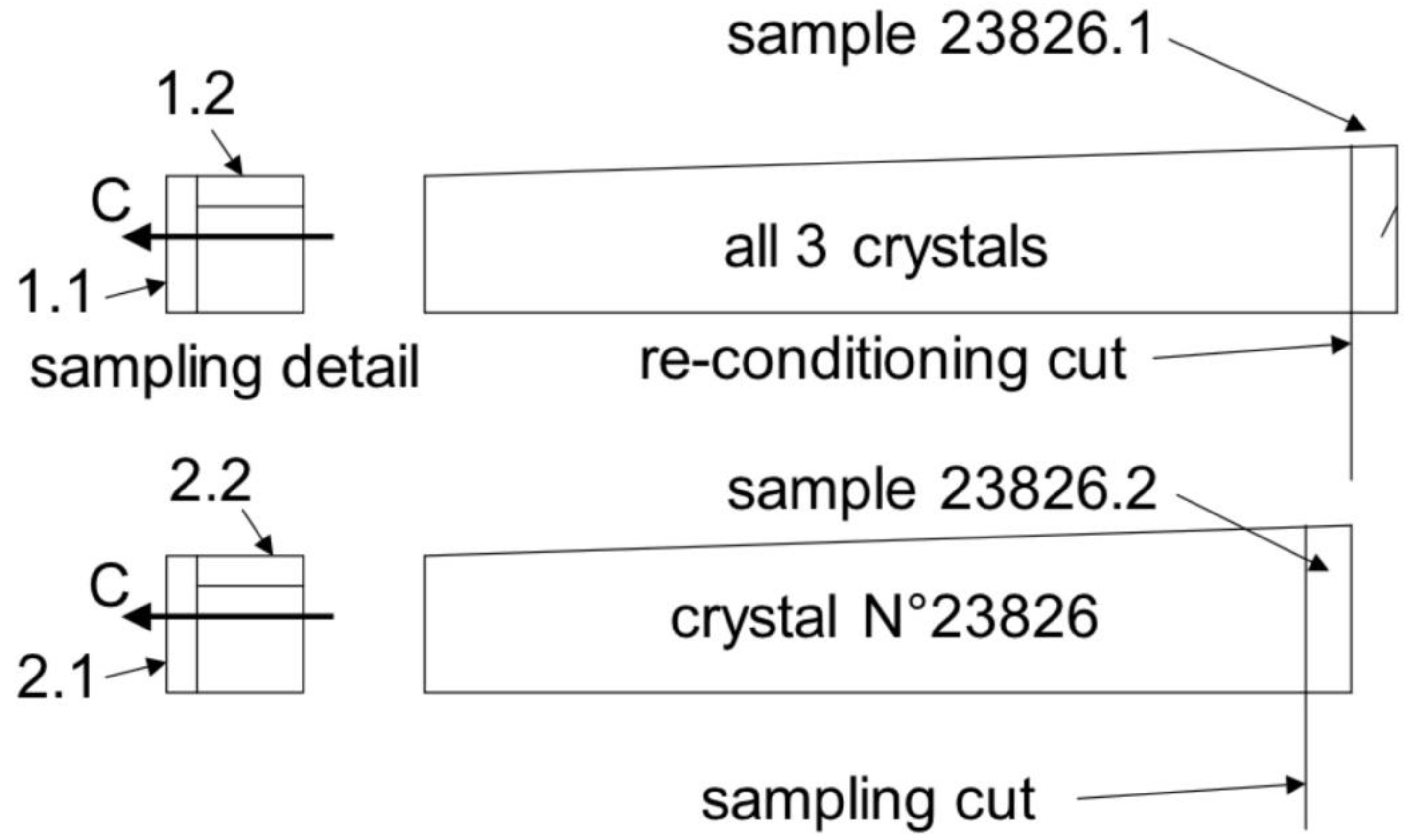
2.3. Sample Selection and Preparation
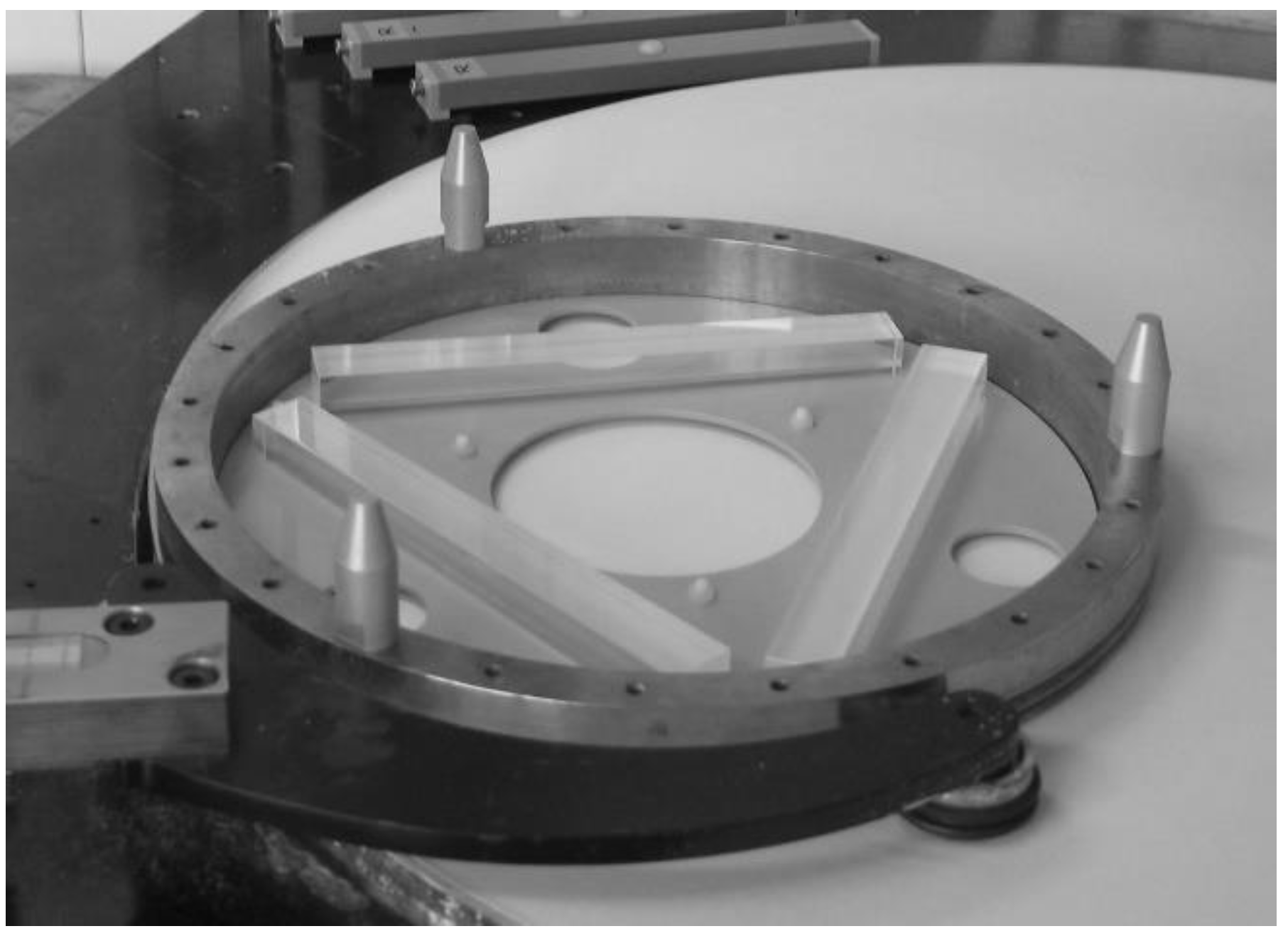
2.4. Grazing Incidence X-ray Diffraction (GID)
2.5. Light Yield (LY) Measurements
3. Results
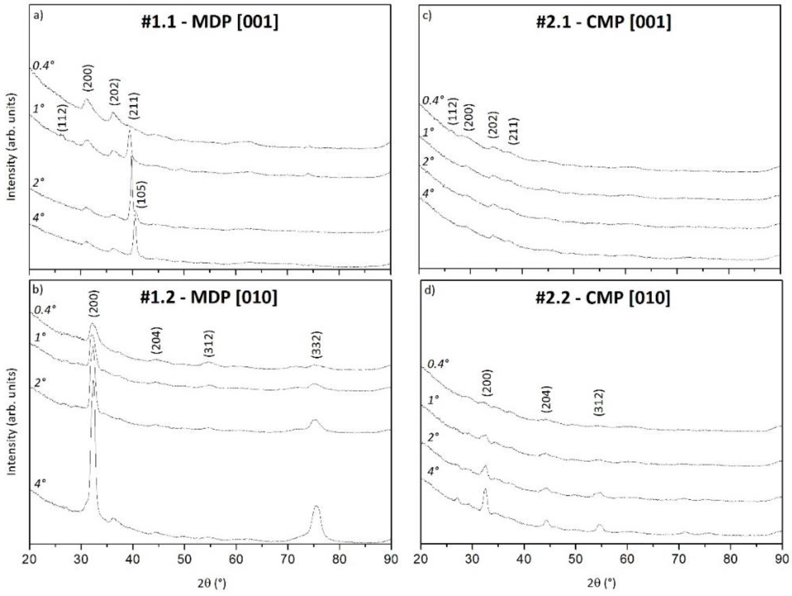
3.1. GID
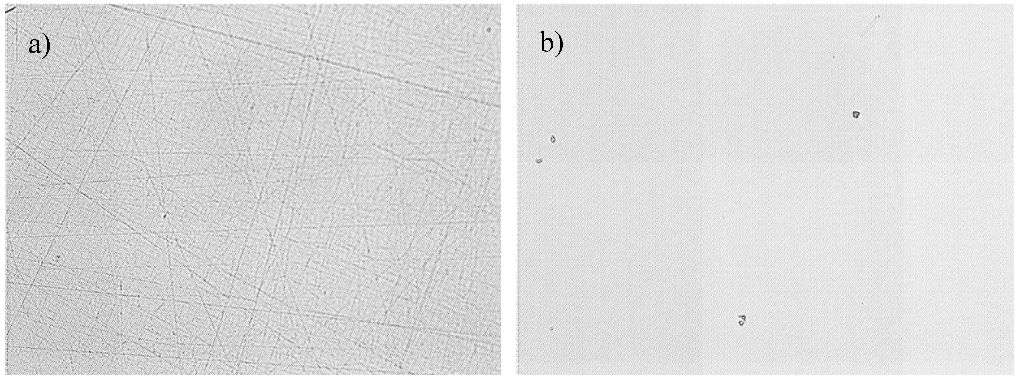
3.2. Surface Finish and Micro-Geometry
3.3. Light Yield (LY)
4. Discussion
5. Conclusions
Author Contributions
Funding
Acknowledgments
Conflicts of Interest
References
- Arduini, G.; Barranco, J.; Bertarelli, A.; Van der Veken, F.; Biancacci, N.; Bruce, R.; Brüning, O.; Buffat, X.; Cai, Y.; Carver, L.R.; et al. High Luminosity LHC: Challenges and plans. J. Instrum. 2016, 11, C12081. [Google Scholar] [CrossRef]
- Andersson, W.I. The PANDA Detector at FAIR. J. Phys. 2016, 770, 012043. [Google Scholar] [CrossRef]
- Apollinari, G.; Béjar Alonso, I.; Brüning, O.; Lamont, M.; Rossi, L. High-Luminosity Large Hadron Collider (HL-LHC). In Preliminary Design Report; CERN: Geneve, Switzerland, 2015. [Google Scholar]
- David, S.; Georgiou, M.; Fysikopoulos, E.; Belcari, N.; Loudos, G. Imaging performance of silicon photomultipliers coupled to BGO and CsI:Na arrays. J. Instrum. 2013, 8, 12008. [Google Scholar] [CrossRef]
- David, S.; Georgiou, M.; Fysikopoulos, E.; Loudos, G. Evaluation of a SiPM array coupled to a Gd3Al2Ga3O12:Ce (GAGG:Ce) discrete scintillator. Phys. Med. 2015, 31, 763–766. [Google Scholar] [CrossRef] [PubMed]
- Lecoq, P. Pushing the Limits in Time-of-Flight PET Imaging. IEEE Trans. Radiat. Plasma Med. Sci. 2017, 1, 473–485. [Google Scholar] [CrossRef]
- Cherry, S.R.; Jones, T.; Karp, J.S.; Qi, J.; Moses, W.W.; Badawi, R.D. Total-Body PET: Maximizing Sensitivity to Create New Opportunities for Clinical Research and Patient Care. J. Nucl. Med. 2018, 59, 3–12. [Google Scholar] [CrossRef] [PubMed]
- Mengucci, P.; Di Cristoforo, A.; Lebeau, M.; Majni, G.; Paone, N.; Pietroni, P.; Rinaldi, D. Surface quality inspection of PbWO4 crystals by grazing incidence X-ray diffraction. Nucl. Instrum. Methods Phys. Res. A 2005, 537, 207–210. [Google Scholar] [CrossRef]
- Mengucci, P.; André, G.; Auffray, E.; Barucca, G.; Cecchi, C.; Chipaux, R.; Cousson, A.; Davì, F.; Di Vara, N.; Rinaldi, D.; et al. Structural, Mechanical and Light Yield Characterisation of Heat Treated LYSO:Ce Single Crystals for Medical Imaging Applications. Nucl. Instrum. Methods Phys. Res. A 2015, 785, 110–116. [Google Scholar] [CrossRef]
- Montalto, L.; Natali, P.P.; Daví, F.; Mengucci, P.; Paone, N.; Rinaldi, D. Characterization of a Defective PbWO4 Crystal Cut Along the a-c Crystallographic Plane: Structural Assessment and a Novel Photoelastic Stress Analysis. J. Instrum. 2017, 12, 12035. [Google Scholar] [CrossRef]
- Natali, P.P.; Montalto, L.; Daví, F.; Mengucci, P.; Ciriaco, A.; Paone, N.; Rinaldi, D. Theoretical and Experimental Evaluation of Piezo-Optic Parameters and Photoelastic Constant in Tetragonal PWO. Appl. Opt. 2018, 57, 730–737. [Google Scholar] [CrossRef] [PubMed]
- Montalto, L.; Rinaldi, D.; Paone, N.; Scalise, L.; Davì, F. Photoelastic Sphenoscopic Analysis of Crystals. Rev. Sci. Instrum. 2016, 87, 015113. [Google Scholar] [CrossRef] [PubMed]
- Daví, F.; Rinaldi, D. Mechanical and Optical Properties of Anisotropic Single-Crystal Prisms. J. Elast. 2015, 120, 197–224. [Google Scholar] [CrossRef]
- Rinaldi, D.; Daví, F.; Montalto, L. On the Photoelastic Constants and the Brewster Law for Stressed Tetragonal Crystals. Math. Methods Appl. Sci. 2018, 41, 3103–3116. [Google Scholar] [CrossRef]
- Mao, R.; Zhang, L.; Zhu, R.Y. Optical and Scintillation Properties of Inorganic Scintillators in High Energy Physics. IEEE Trans. Nucl. Sci. 2008, 55, 2425–2431. [Google Scholar] [CrossRef] [Green Version]
- Vlassak, J.J. A Model for Chemical–Mechanical Polishing of a Material Surface Based on Contact Mechanics. J. Mech. Phys. Solids 2004, 52, 847–873. [Google Scholar] [CrossRef]
- Diehl, S.; Brinkmann, K.T.; Drexler, P.; Dormenev, V.; Novotny, R.W.; Rosenbaum, C.; Zaunick, H.G. Impact of Non-Uniformity in Light Collection on the Energy Resolution of the PANDA Electromagnetic Calorimeter at Photon Energies Below 1 GeV. J. Phys. 2017, 928, 012040. [Google Scholar] [CrossRef] [Green Version]
- Borgia, B.; Baccaro, S. Tungstate Crystals: Proceedings of the International Workshop on Tungstate Crystals; Università degli studi La Sapienza: Rome, Italy, 1999; ISBN 8887242100. [Google Scholar]
- Diehl, S.; Bremer, D.; Brinkmann, K.T.; Dormenev, V.; Eissner, T.; Novotny, R.W.; Rosenbaum, C.; Zaunick, H.G. Measurements and Optimization of the Light Collection Uniformity in Strongly Tapered PWO Crystals of the PANDA Detector. Nucl. Instrum. Methods Phys. Res. A 2017, 857, 1–6. [Google Scholar] [CrossRef]
- Wapler, W.; Juchem, H.O. Diamond abrasive for Machining glass. Ind. Diam. Rev. 1987, 4, 159–162. [Google Scholar]
- Huerta, M.; Malkin, S. Grinding of Glass: The Mechanics of the Process. J. Eng. Ind. 1976, 459–467. [Google Scholar] [CrossRef]
- Malkin, S.; Ritter, J.E. Grinding Mechanisms and Strength Degradation for Ceramics. J. Eng. Ind. 1989, 111, 167–174. [Google Scholar] [CrossRef]
- Senguttuvan, N.; Ishii, M.; Tanji, K.; Kittaka, T.; Usuki1, Y.; Kobayashi, M.; Nikl, M. Influence of Annealing on the Optical Properties of PbWO4 Single Crystals Grown by the Bridgman Method. Jpn. J. Appl. Phys. 2000, 39, 5134. [Google Scholar] [CrossRef]
- Mao, R.; Zhang, L.; Zhu, R.Y. Quality of Mass-Produced Lead Tungstate Crystals. In Proceedings of the 2003 IEEE Nuclear Science Symposium, Conference Record (IEEE Cat. No.03CH37515), Portland, OR, USA, 19–25 October 2003. [Google Scholar] [CrossRef]
- Kasap, S.O. Optoelectronics and Photonics: Principles and Practices, 2nd ed.; University of Saskatchewan: Saskatoon, SK, Canada; Pearson: London, UK, 2013; ISBN 13 9780201610871. [Google Scholar]


| MDP Finishing | ||
| A—Original lapping | B—Mechanical diamond polishing | |
| abrasive | 28 µm corundum in water emulsion | 2 µm polycrystalline. diamond water emulsion |
| time-velocity-pressure | 5 min - - manual | 10 min-60 rpm-2N/cm2 |
| removal [001] | 50 µm nominal | # 10 µm |
| removal [010] | 50 µm nominal | # 10 µm |
| CMP Finishing | ||
| C—Re-conditioning lapping | D—Chemical mechanical polishing | |
| abrasive | 15 µm polycrystalline diamond water emulsion | colloidal silica in 50% water dilution |
| Time-velocity-pressure | 10 min-60 rpm-2 N/cm2 | 10 min-60 rpm-2 N/cm2 |
| removal [001] | 40 µm average | # 10 µm |
| removal [010] | 68 µm average | # 10 µm |
| Treatment Sequence for MDP Finishing | Treatment Sequence for CMP Finishing | ||
|---|---|---|---|
| Operation | Details | Operation | Details |
| Starting state | conventional lapping (A) & polishing (B) of 3 side-faces | Lapping (C) | 3 side-faces |
| Sampling 1 of crystal 1 | Cutting 1.1 and.1.2 | CMP (D) | 3 side-faces |
| GID observations | Plots 1.1 and.1.2 | Sampling 2 of crystal 1 | Cutting 2.1 and 2.2 |
| Optical measurement | Crystals 2 & 3 | GID observations | Plots 2.1 and 2.2 |
| Sample | Treatment | LY (p.e./MeV) | FNUF (%/X0) | RNUF (%/X0) | |||
|---|---|---|---|---|---|---|---|
| Average | σ | Average | σ | Average | σ | ||
| #38138 | MDP | 12.18 | 0.07 | 0.020 | 0.023 | −0.056 | 0.046 |
| CMP | 12.28 | 0.06 | −0.180 | 0.020 | −0.012 | 0.040 | |
| #32134 | MDP | 13.40 | 0.13 | 0.032 | 0.040 | 0.077 | 0.080 |
| CMP | 13.69 | 0.07 | −0.076 | 0.020 | 0.115 | 0.040 | |
© 2018 by the authors. Licensee MDPI, Basel, Switzerland. This article is an open access article distributed under the terms and conditions of the Creative Commons Attribution (CC BY) license (http://creativecommons.org/licenses/by/4.0/).
Share and Cite
Rinaldi, D.; Montalto, L.; Lebeau, M.; Mengucci, P. Influence of a Surface Finishing Method on Light Collection Behaviour of PWO Scintillator Crystals. Photonics 2018, 5, 47. https://doi.org/10.3390/photonics5040047
Rinaldi D, Montalto L, Lebeau M, Mengucci P. Influence of a Surface Finishing Method on Light Collection Behaviour of PWO Scintillator Crystals. Photonics. 2018; 5(4):47. https://doi.org/10.3390/photonics5040047
Chicago/Turabian StyleRinaldi, Daniele, Luigi Montalto, Michel Lebeau, and Paolo Mengucci. 2018. "Influence of a Surface Finishing Method on Light Collection Behaviour of PWO Scintillator Crystals" Photonics 5, no. 4: 47. https://doi.org/10.3390/photonics5040047