Article

Ar+-Implanted Si-Waveguide Photodiodes for Mid-Infrared Detection

1
Photonics Research Center, United States Military Academy, West Point, NY 10996, USA
2
Department of Electrical Engineering, Columbia University, 500 W. 120th Street, New York, NY 10027, USA
3
Center for Functional Nanomaterials, Brookhaven National Laboratory, PO Box 5000, Upton, NY 11973, USA
4
College of Nanoscale Science and Engineering, SUNYPOLY, Albany, NY 12203, USA
5
Department of Electrical and Systems Engineering, University of Pennsylvania, 200 S. 33rd Street, Philadelphia, PA 19104, USA
6
IBM T. J. Watson Research Center, 1101 Kitchawan Rd., Yorktown Heights, NY 10598, USA
7
Microelectronics Sciences Laboratories, Columbia University, 500 W. 120th Street, New York, NY 10027, USA
*
Author to whom correspondence should be addressed.
Photonics 2016, 3(3), 46; https://doi.org/10.3390/photonics3030046
Submission received: 30 June 2016 / Revised: 18 July 2016 / Accepted: 22 July 2016 / Published: 27 July 2016
(This article belongs to the Special Issue Advanced Photodetectors Devices and Technologies)

Abstract

:
Complementary metal-oxide-semiconductor (CMOS)-compatible Ar+-implanted Si-waveguide p-i-n photodetectors operating in the mid-infrared (2.2 to 2.3 µm wavelengths) are demonstrated at room temperature. Responsivities exceeding 21 mA/W are measured at a 5 V reverse bias with an estimated internal quantum efficiency of 3.1%–3.7%. The dark current is found to vary from a few nanoamps down to less than 11 pA after post-implantation annealing at 350 °C. Linearity is demonstrated over four orders of magnitude, confirming a single-photon absorption process. The devices demonstrate a higher thermal processing budget than similar Si+-implanted devices and achieve higher responsivity after annealing up to 350 °C.

Graphical Abstract

1. Introduction

As the maximum data rate of single-mode fiber reaches limits imposed by spurious optical nonlinearities, multiple efforts have been focused on methods to increase overall system capacity. For example, aggregate data rates of 1.6 Tb/s over 1 km have been demonstrated utilizing orbital angular momentum multiplexing [1] while even higher data rates of over 2 Pb/s have been demonstrated utilizing multicore fibers [2]. Efforts to increase capacity have also been applied to photonic integrated circuits, such as, for example, the use of multimode silicon waveguides to support an aggregate data rate of 60 Gb/s [3,4]. In these examples, while spatial-mode-division multiplexing techniques were a key component to achieving the high capacities in each of these links, wavelength division multiplexing (WDM) also played a critical role. Thus, in order to continue satisfying data-rate demands, the focus should be on not only utilizing and improving recent multiplexing techniques, but also on improving more common techniques such as WDM. One straight-forward approach to achieving increased data rates for WDM is to expand into additional wavelength bands; this approach includes reaching further into the infrared, as demonstrated in [5].
While the addition of long wavelengths offers the potential for increased capacity, it also offers some important challenges in realizing many of the components necessary for a high-performance guided-wave system. For example, recent advancements in thulium-doped fiber amplifiers have made possible the needed laser sources while the development of numerous passive Si photonic components working at wavelengths beyond 1.55 µm have extended basic Si circuits into the mid-infrared (2–2.5 µm) [6,7,8,9,10,11,12,13,14]. However, other devices remain to be fully developed. For example, in the case of photodetectors (PDs), the large intrinsic band gap of Si has led to the development of multiple heterogeneous PD technologies [6,7] capable of operating in this range; however, additional materials processing beyond what is done in a standard complementary metal-oxide-semiconductor (CMOS) fabrication line is required. An alternative, i.e., the class of ion-implanted Si PDs, which uses implant-induced vacancies, first showed promise operating at 1.55 µm [15,16] including advances such as increased responsivities [17] and error-free data detection at 10 Gb/s [18]. These ion-implanted PDs have been utilized for wavelengths beyond 1.55 µm with the first demonstration of error-free detection of 1 Gb/s data at 1.9 µm [19] followed by 20 Gb/s operation at 1.96 µm [8]. Applications for these detectors can range from their use as auto-correlators [9] to fast power monitors [10]. Responsivities between 5 mA/W and 300 mA/W have been achieved [8,12,13,14]. To date, the majority of these PDs have relied upon the Si divacancy defect for detection. However, overcoming the low thermal stability of the Si divacancy [20,21,22,23,24] remains a challenge for integrating these devices due to the low thermal processing budget after ion implantation; this low thermal budget limits any form of additional fabrication processing. Recently, Ar+ implantation has been shown to have higher thermal stability than devices relying upon the divacancy defect [23], and has the potential to alleviate the thermal stability issues while providing a route to a monolithic Mid-IR detection for silicon photonics.
In this work, we study the linearity, responsivity, and thermal stability of Ar+-implanted monolitihic Si-waveguide PDs over a 2.2–2.3 µm wavelength range and compare these devices with similar Si+-implanted devices. In particular, the Ar+ devices show a higher optical absorption coefficient and higher thermal stability than similarly structured and implanted Si+ devices while retaining similar internal quantum efficiencies (IQE). Our devices show a peak responsivity between 20 and 25 mA/W for a 3 mm long PD, using a reverse bias of 5 V; our results compare very favorably with the best performing Si+-implanted devices in the literature [8,12,13,14], and nearly double the peak responsivity seen for similar Si+-implanted devices operating under the same conditions.

2. Materials and Methods
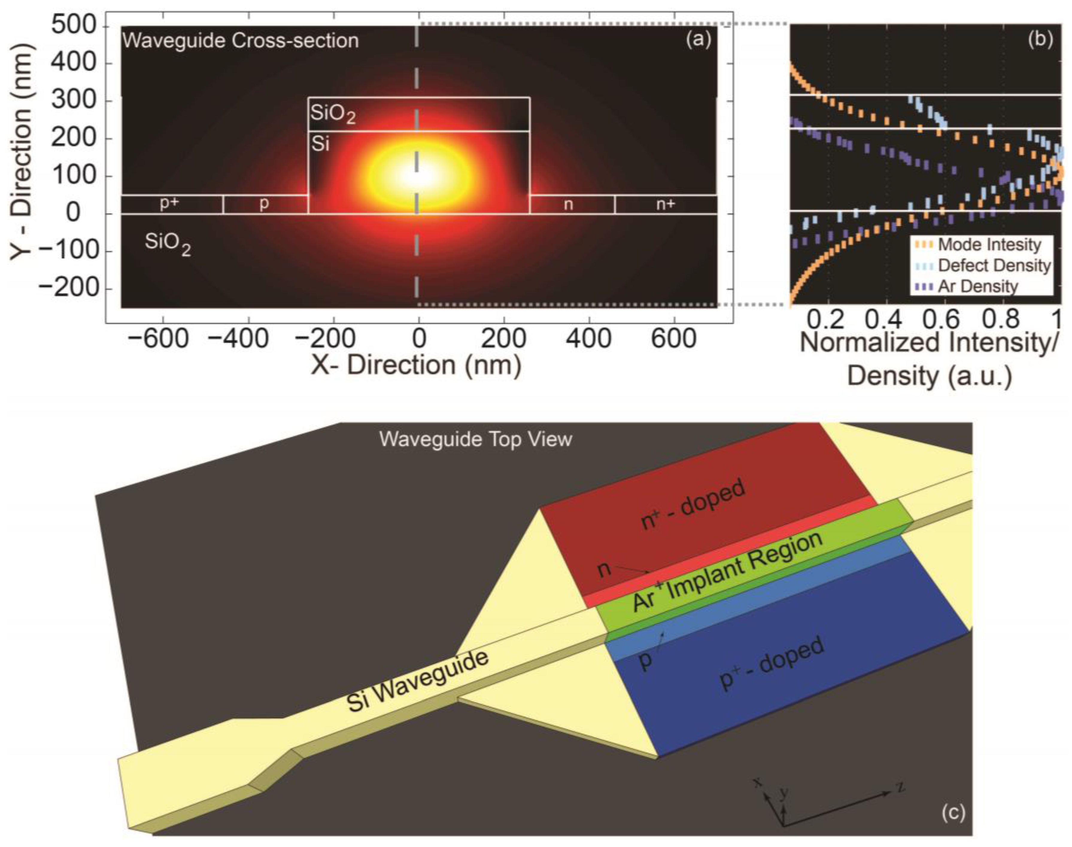
2.1. Fabrication

The Si-waveguide p-i-n devices were fabricated at MIT Lincoln Laboratory using the procedure discussed in [16]. Each device consisted of a Si channel waveguide with dimensions of 520 × 220 nm. The diode portion of the devices consisted of the channel waveguide with the addition of 50 nm high “wings” doped in the p+ (boron), n+ (phosphorus) and p, n regions to concentrations of 1019 cm−3 and 1018 cm−3, respectively. As indicated in Figure 1, the p and n regions were located near the channel waveguide, with a total length of approximately 200 nm. Adjacent to the p and n regions were p+ and n+ regions, respectively, upon which the electrical contacts were placed. The contacts consisted of a 300 nm Al layer on a 10 nm W adhesion layer. Light was coupled onto and off the chip through 5 µm-wide fan-out tapers. The waveguides were adiabatically tapered both to the couplers, going from 5 µm to 520 nm over a propagation length of 450 µm, and then into the p-i-n waveguide section, which contained “wings” over 100 µm in length.
To pattern the photodiodes, the device array was then masked using photolithography and a 1 µm layer of Shipley S1811 resist with openings of 250 µm and 3 mm over the p-i-n diode section of the devices. The devices were then subsequently implanted with Ar+ at an energy of 240 keV.
Unlike the Si+-implanted devices previously fabricated in [12] or the Zn+-implanted devices in [13], the Ar+ implantation energy was chosen to place both the peak of the defect density and the peak Ar ion concentration in the waveguide. In previously fabricated Si+-implanted devices, the energy was chosen to place the peak of the defect density in the center of the waveguide [24] resulting in a large portion of the Si ions in the substrate. However, since the vacancies are highly mobile at the annealing temperatures used in [20], a nearly uniform distribution of defects and Ar ions throughout the channel section of the waveguide was expected after the annealing process. The exact ion energies and doses chosen for the implantation step were based on prior reports of ion-induced defects [12,23,24] and Stopping Range of Ions in Matter (SRIM) calculations [25]. Figure 1b shows the results of the SRIM calculations for both the initial (pre-annealing) defect profile and the Ar+-ion profile overlapping with the modal intensity calculated at the center of the channel waveguide. Post-processing after the initial implantation exposed the chips to a temperature of approximately 80 °C, at which initial device parameters were measured. Subsequent annealing steps started at 150 °C for 10 min in an ambient atmosphere, after which the device measurements were repeated. Further annealing was conducted at temperatures of 200 °C, 250 °C, 300 °C, and 350 °C, again for 10 min in atmosphere at each step, with the final annealing temperature limited by the reflow temperature of the Al electrical contacts. Following each anneal, the device parameters were again measured.

2.2. Experimental Setup

An external-cavity Cr2+:ZnSe laser, which could be tuned across a wavelength range from λ = 2.2 to 2.4 µm, served as the optical source for detector measurements. Power from the laser was coupled into a standard single-mode fiber (SMF) patch cord utilizing a fiber collimator. The patch cord ran through a polarization rotator (PR) which was connected to a lens-tapered-fiber (LTF) with a 2.5 µm spot size at 1550 nm to couple light onto the chip via the fan-out tapered coupler into the waveguide and then to the Ar+ implanted p-i-n diode region. The PR was used to ensure that the light was polarized to excite the TE mode in the waveguide, providing maximum modal overlap with the implanted region of the device. Light was coupled out of the PD in a retrograde manner, going from the fan-out taper to the LTF and then into a Yokogawa AQ6375 infrared optical spectrum analyzer (OSA) for power measurement.
Prior to taking measurements, the system losses were characterized, including losses through the patch cord, the LTFs, the couplers, and any waveguide section, prior to reaching the detector. Optical input power was measured at the connection of the SMF patch cord and the LTF with our infrared OSA. Optical output power was coupled out of the chip using a LTF, and was measured at the end of a 1 m section of SMF patch cord by the OSA. Waveguide and PD losses were characterized utilizing the cutback method on varying lengths of waveguide sections and un-implanted PDs. Five consecutive measurements were done on multiple devices for each chip to calculate an average total loss and standard deviation. Loss was initially measured in dB and then converted to the appropriate ratio of Pout/Pin prior to averaging and thus finding the standard deviation; this measurement assumed a normally distributed error versus a log-normal distribution. The results gave a total loss prior to the PD, including LTF loss, coupling loss, and waveguide loss. The total input optical power losses prior to the PD was 11.2 ± 0.76 dB for these devices.

3. Results

3.1. Experimental Setup

Figure 2a shows the photocurrent and dark current for the 250 µm device after annealing to 300 °C and then to 350 °C, which were the temperatures that were found to show the highest responsivity. These annealing temperatures resulted not only in an increase in responsivity, but also in a decrease in dark current by over two orders of magnitude from the initial measurements taken after annealing at 80 °C. Further, when the bias voltage was reduced to 0 V, these devices had 41% of the measured photocurrent compared to that obtained at a bias of 5 V, while the dark current dropped to less than 11 pA, resulting in over a six order of magnitude difference between the photo- and the dark current. With such low dark currents and high responsivities, these detector circuits are ideal for use in applications such as ring resonator stabilization [26].
The linearity of the implanted detectors was measured after a 250 °C and then a 350 °C annealing temperature over a four order of magnitude variation in optical power as seen in Figure 2b. From Figure 3b, the Ar+-implanted devices demonstrated no loss in responsivity after the 250 °C anneal as was seen in the Si+-implanted devices, initiating the more thorough linearity measurements done here, with measurements taken at 300 °C and 350 °C with the 350 °C data presented.

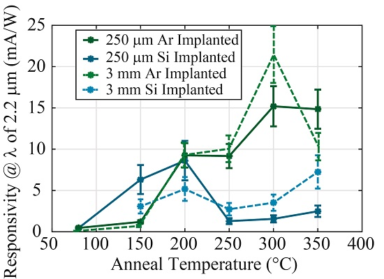
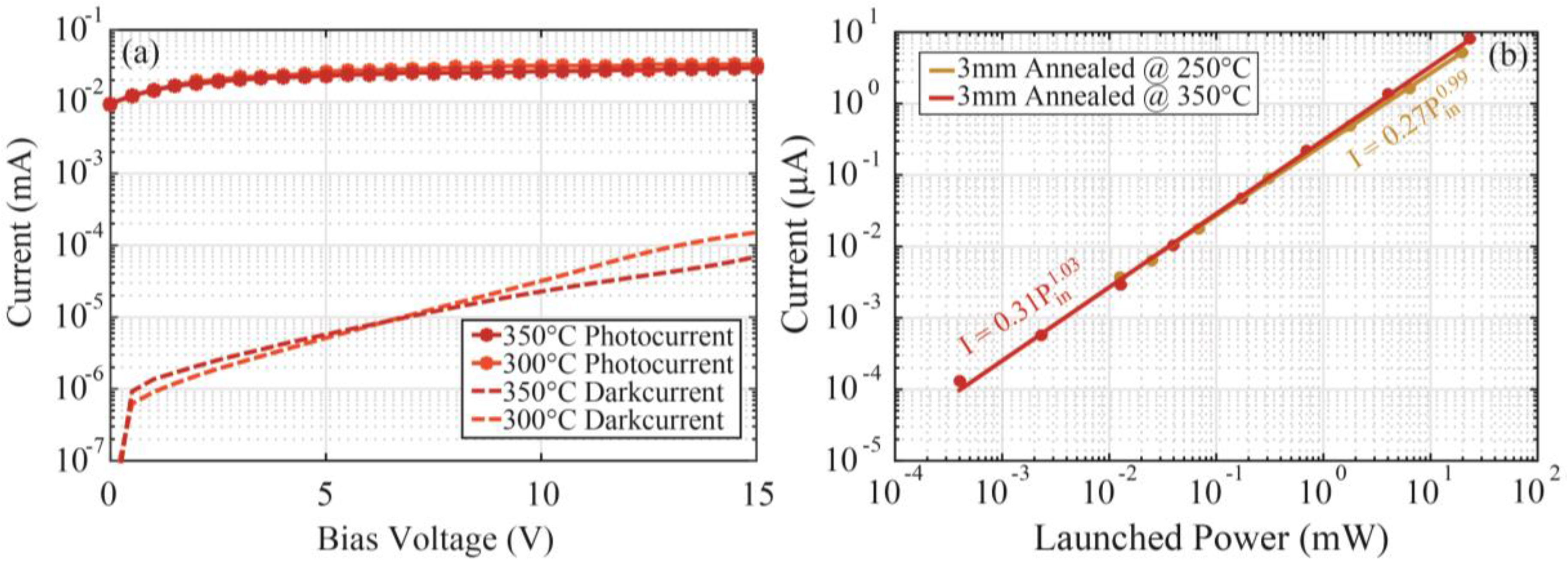
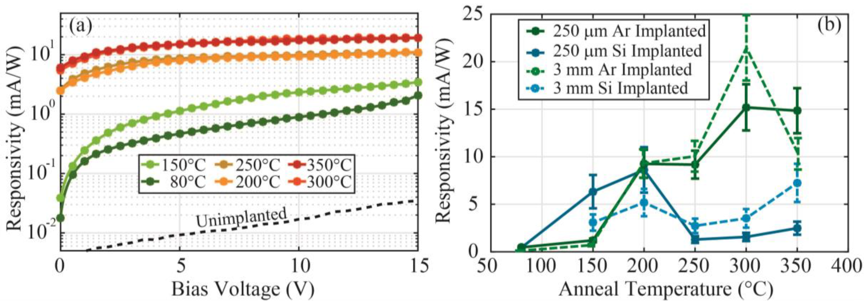
3.2. Experimental Results

Responsivity was measured both for variations in bias voltage and annealing temperature, as shown in Figure 3a,b. Responsivity was calculated as = I p h o t o / ( P i n c ± Δ P i n c ) , where Iphoto is the illuminated current minus the dark current, and Pinc was the calculated average incident power on the photodiode that was found by subtracting out the system losses, as discussed above. The error bars were calculated using propagation of error rules and based on the standard deviation of the input power, as determined from the above measurements.
The responsivity vs. annealing temperature (as seen in Figure 3b) for the Ar+-implanted devices is plotted with the same data as provided in [12] for Si+-implanted devices. As seen in [23] for 1550 nm, the Ar+-implanted devices generally showed increasing responsivity with increasing annealing temperature and lack the characteristic peak at 200 °C seen in the Si+-implanted devices. Note that during measurements, an anomaly was found for the 3 mm device such that the responsivity after annealing at 350 °C was significantly lower than the responsivity after annealing at 300 °C. After inspection of the device, it was found that the waveguide was mechanically damaged; as a result the additional measurements below were made using the 250 µm waveguide device.
Figure 4 shows the responsivity of the 250-µm-long PD after annealing at 350 °C, as measured over wavelengths from 2.2 µm to 2.3 µm. Consistent with results reported for other implanted devices [8,12,13], the measured responsivity showed a significant decrease with increasing wavelength, i.e., decreasing by more than 6 dB as the wavelength increased from 2.2 µm to 2.3 µm.
The IQE at 2.2 µm was calculated for the devices utilizing the measured parasitic losses, modal absorption coefficients and the responsivities following the procedures in [9,10]. The calculated IQE was found to be nearly equal for different PD types, with the 3 mm PD annealed at 300 °C having a quantum efficiency of 3.70 ± 0.70% and the 250 µm PD annealed at 350 °C having a quantum efficiency of 3.11 ± 0.69%. These results compared favorably to the IQEs calculated in [12] for Si+-implanted devices, which were found to range from 2.7 ± 0.9% to 4.5 ± 1.1%. The reason for the increase in responsivity in the Ar+-implanted PDs compared to the Si+-implanted PDs is due to increased absorption. In particular, the Si+-implanted PDs have measured absorption coefficients ranging from 31 to 66 dB/cm, while the Ar+-implanted PDs have measured absorption coefficients ranging from 115 to 156 dB/cm.

4. Discussion and Conclusions

Integrated Ar+-implanted Si-waveguide photodetectors have been demonstrated and characterized for use in the mid-IR. While similar detectors have been demonstrated utilizing B, Si, and Zn ion implantation [7,9,10,11], the Ar+-implanted devices have demonstrated improved low bias (~5 V or less) operation. The responsivities of these Ar+-implanted devices were measured to be as high as 21.3 mA/W at a wavelength of 2200 nm and with a 5 V reverse bias; to the best of our knowledge this is the highest responsivity reported at this wavelength and bias for ion-implanted Si-waveguide photodiodes. The PDs also displayed excellent characteristics at even lower biases, retaining 41% of their responsivity in reducing the bias from 5 V to no bias while also maintaining very low dark currents. For example, the minimum dark current (with the waveguide exposed to ambient room light) was 11 pA at a 0 V bias, and only 5 nA at a 5 V bias. In addition, the measured IQEs were found to be similar to previously reported Si+-implanted PDs, with the increases in responsivity being attributed to increases in the absorption coefficient, another key characteristic necessary for decreasing device lengths. Although these responsivities are significantly lower than values reported for heterogeneously integrated detectors based on binary materials, their simple fabrication procedure, low dark current, and CMOS compatibility make these devices desirable for a variety of integrated Si photonic systems operating in the mid-infrared.
Our results above are also consistent with previously measured absorption properties of Ar+-implanted Si, which is known to have defects with an energy level spectrum that is similar to that of the Si divacancy defect [23]. However, note that these Ar+-implantation induced defects have shown higher thermal stability than that of the Si divacancy defect and in fact anneal out at temperatures greater than 350 °C [23], consistent with the above results showing improved detection at annealing temperatures of 300 °C and 350 °C. With higher thermal stability, our devices allow for an increased thermal budget post processing, thus offering more flexibility in device fabrication.
Although many of these ion implanted PDs have demonstrated improved performance when operating in the avalanche regime [8,27], we did not see any indication of improved performance with higher biases on these or in our previous work with Si+-implanted PDs [12]. The lack of clear avalanche multiplication is believed to be due to the device structure and implantation, as there was significant overlap in the doped “wings” of the device and the implantation region. Further research will work towards better fabrication tolerances to prevent overlapping between doped “wing” region and ion implantation region.
While this study covered the basic operating parameters of these devices, there are still several areas to continue to examine. One key limitation was in the design of the PD; the Al contacts limited the maximum annealing temperature to 350 °C, with reflow starting to occur at a temperature of 400 °C. Future studies will look at annealing beyond 350 °C to further characterize the device parameters after higher temperature annealing. Device fabrication parameters also need to be studied to optimize performance. The parameters chosen for implantation energy and dose were based on SRIM calculations and our previous work with Si+-implantation. With an in-depth parametric study of implant dose and energy, device performance should continue to improve.

Acknowledgments

The research here was carried out in part at the Center for Functional Nanomaterials, Brookhaven National Laboratory, which is supported by the U.S. Department of Energy, Office of Basic Energy Sciences, under Contract No. DE-AC02-98CH10886. The authors also acknowledge support from the Semiconductor Research Corporation/Intel Ph.D Fellowship and the Columbia Optics and Quantum Electronics IGERT under NSF grant DGE-1069420. The authors would also like to acknowledge Michael W. Geis and Steven J. Spector for assistance in device fabrication.

Author Contributions

B.S. conceived of the devices and measurements and performed simulations; B.S., C.P.C., and R.R.G wrote the paper; B.S. and C.P.C. performed the measurements; B.S., M.L., and A.S. prepped the chip for ion implantation; B.S. and H.B. performed the ion implantation, with H.B. supplying the facilities for ion implantation; R.R.G. contributed automation software for measurements; K.B. and W.M.J.G. contributed test equipment and lab space; R.M.O. contributed test equipment, lab space, and funding.

Conflicts of Interest

The authors declare no conflict of interest.

References

  1. Bozinovic, N.; Yue, Y.; Ren, Y.; Tur, M.; Kristensen, P.; Huang, H.; Willner, A.E.; Ramachandran, S. Terabit-Scale Orbital Angular Momentum Mode Division Multiplexing in Fibers. Science 2013, 340, 1545–1548. [Google Scholar] [CrossRef] [PubMed]
  2. Puttnam, B.J.; Luís, R.S.; Klaus, W.; Sakaguchi, J.; Mendinueta, J.-M.D.; Awaji, Y.; Wada, N.; Tamura, Y.; Hayashi, T.; Hirano, M.; et al. 2.15 Pb/s Transmission Using a 22 Core Homogeneous Single-Mode Multi-Core Fiber and Wideband Optical Comb. In Proceedings of the 2015 European Conference on Optical Communication, Valencia, Spain, 27 September–1 October 2015.
  3. Driscoll, J.B.; Chen, C.P.; Grote, R.R.; Souhan, B.; Dadap, J.I.; Stein, A.; Lu, M.; Bergman, K.; Osgood, R.M. A 60 Gb/s MDM-WDM Si photonic link with <0.7 dB power penalty per channel. Opt. Express 2014, 22, 18543–18555. [Google Scholar] [PubMed]
  4. Chen, C.P.; Driscoll, J.B.; Grote, R.R.; Souhan, B.; Osgood, R.M., Jr.; Bergman, K. Mode and Polarization Multiplexing in a Si Photonic Chip at 40Gb/s Aggregate Data Bandwidth. IEEE Photon. Technol. Lett. 2015, 27, 22–25. [Google Scholar] [CrossRef]
  5. Ophir, N.; Lau, R.K.W.; Ménard, M.; Salem, R.; Padmaraju, K.; Okawachi, Y.; Lipson, M.; Gaeta, A.L.; Bergman, K. First Demonstration of a 10-Gb/s RZ End-to-End Four-Wave-Mixing Based Link at 1884 nm Using Silicon Nanowaveguides. IEEE Photon. Technol. Lett. 2012, 24, 276–278. [Google Scholar] [CrossRef]
  6. Roelkens, G.; Dave, U.; Gassenq, A.; Hatasan, N.; Hu, C.; Kuyken, B.; Leo, F.; Malik, A.; Muneeb, M.; Ryckeboer, E.; et al. Silicon-based heterogeneous photonic integrated circuits for the mid-infrared. Opt. Mater. Express 2013, 3, 1523–1536. [Google Scholar] [CrossRef]
  7. Lin, P.T.; Singh, V.; Wang, J.; Lin, H.; Hu, J.; Richardson, K.; Musgraves, J.D.; Luzinov, I.; Hensley, J.; Kimerling, L.C.; et al. Si-CMOS compatible materials and devices for mid-IR microphotonics. Opt. Mater. Express 2013, 3, 1474–1487. [Google Scholar] [CrossRef]
  8. Ackert, J.J.; Thomson, D.J.; Shen, L.; Peacock, A.C.; Jessop, P.E.; Reed, G.T.; Mashanovich, G.Z.; Knights, A.P. High-speed detection at two micrometres with monolithic silicon photodiodes. Nat. Photon. 2015, 9, 393–396. [Google Scholar] [CrossRef]
  9. Xu, C.; Roth, J.M.; Knox, W.H.; Bergman, K. Ultra-sensitive autocorrelation of 1.5 μm light with single photon counting silicon avalanche photodiode. Electron. Lett. 2002, 38, 86–88. [Google Scholar] [CrossRef]
  10. Logan, D.F.; Velha, P.; Sorel, M.; de La Rue, R.M.; Jessop, P.E.; Knights, A.P. Monitoring and Tuning Micro-Ring Properties Using Defect-Enhanced Silicon Photodiodes at 1.55 μm. IEEE Photon. Technol. Lett. 2012, 24, 261–263. [Google Scholar] [CrossRef]
  11. Van Camp, M.A.; Assefa, S.; Gill, D.M.; Barwicz, T.; Shank, S.M.; Vlasov, Y.A.; Green, W.M. Demonstration of Electrooptic Modulation at 2165 nm Using a Silicon Mach-Zehnder Interferometer. Opt. Express 2012, 20, 28009–28016. [Google Scholar] [CrossRef] [PubMed]
  12. Souhan, B.; Grote, R.R.; Chen, C.P.; Huang, H.-C.; Driscoll, J.B.; Lu, M.; Stein, A.; Bakhru, H.; Bergman, K.; Green, W.M.J.; et al. Si+-implanted Si-wire waveguide photodetectors for the mid-infrared. Opt. Express 2014, 22, 27415–27424. [Google Scholar] [CrossRef] [PubMed]
  13. Grote, R.R.; Souhan, B.; Ophir, N.; Driscoll, J.B.; Bergman, K.; Bakhru, H.; Green, W.M.J.; Osgood, R.M. Extrinsic Photodiodes for Integrated Mid-Infrared Silicon Photonics. Optica 2014, 1, 264–267. [Google Scholar] [CrossRef]
  14. Thomson, D.J.; Shen, L.; Ackert, J.J.; Huante-Ceron, E.; Knights, A.P.; Nedeljkovic, M.; Peacock, A.C.; Mashanovich, G.Z. Optical detection and modulation at 2 µm–2.5 µm in silicon. Opt. Express 2014, 22, 10825–10830. [Google Scholar] [CrossRef] [PubMed]
  15. Geis, M.W.; Spector, S.J.; Grein, M.E.; Schulein, R.T.; Yoon, J.U.; Lennon, D.M.; Deneault, S.; Gan, F.; Kaertner, F.X.; Lyszczarz, T.M. CMOS-Compatible All-Si High-Speed Waveguide Photodiodes with High Responsivity in Near-Infrared Communication Band. IEEE Photon. Technol. Lett. 2007, 19, 152–154. [Google Scholar] [CrossRef]
  16. Geis, M.W.; Spector, S.J.; Grein, M.E.; Schulein, R.T.; Yoon, J.U.; Lennon, D.M.; Wynn, C.M.; Palmacci, F.; Gan, F.; Kaertner, F.X.; et al. All silicon infrared photodiodes: Photo response and effects of processing temperature. Opt. Express 2007, 15, 16886–16895. [Google Scholar] [CrossRef] [PubMed]
  17. Geis, M.W.; Spector, S.J.; Grein, M.E.; Yoon, J.U.; Lennon, D.M.; Lyszczarz, T.M. Silicon waveguide infrared photodiodes with >35 GHz bandwidth and phototransistors with 50 AW−1 response. Opt. Express 2009, 17, 5193–5204. [Google Scholar] [CrossRef] [PubMed]
  18. Grote, R.R.; Padmaraju, K.; Souhan, B.; Driscoll, J.B.; Bergman, K.; Osgood, R.M. 10 Gb/s Error-Free Operation of All-Silicon Ion-Implanted-Waveguide Photodiodes at 1.55 µm. IEEE Photon. Technol. Lett. 2013, 25, 67–70. [Google Scholar] [CrossRef]
  19. Souhan, B.; Chen, C.P.; Grote, R.R.; Driscoll, J.B.; Ophir, N.; Bergman, K.; Osgood, R.M. Error-Free Operation of an All-Silicon Waveguide Photodiode at 1.9 µm. IEEE Photon. Technol. Lett. 2013, 25, 2031–2034. [Google Scholar] [CrossRef]
  20. Deenapanray, P.N.K.; Auret, F.D.; Ridgway, M.C.; Goodman, S.A.; Myburg, G.; Malherbe, J.B. Deep level transient spectroscopy characterization of 1 keV He, Ne, and Ar ion bombarded, epitaxially grown n-Si. J. Appl. Phys. 1998, 84, 2565–2570. [Google Scholar] [CrossRef]
  21. Fan, H.Y.; Ramdas, A.K. Infrared Absorption and Photoconductivity in Irradiated Silicon. J. Appl. Phys. 1959, 30, 1127–1134. [Google Scholar] [CrossRef]
  22. Dannefaer, S.; Avalos, V.; Kerr, D.; Poirier, R.; Shmarovoz, V.; Zhang, S.H. Annealing of electron-, proton-, and ion-produced vacancies in Si. Phys. Rev. B 2006, 73. [Google Scholar] [CrossRef]
  23. Souhan, B.; Grote, R.; Driscoll, J.; Bakhru, H.; Osgood, R.M. CMOS Compatible Argon-Ion-Implanted C-Band Silicon waveguide Photodetector. In Proceedings of the Conference on Lasers and Electro-Optics, Technical Digest (online), San Jose, CA, USA, 9–14 June 2013.
  24. Souhan, B.; Grote, R.R.; Driscoll, J.B.; Lu, M.; Stein, A.; Bakhru, H.; Osgood, R.M. Metal-semiconductor-metal ion-implanted Si waveguide photodetectors for C-band operation. Opt. Express 2014, 22, 9150–9158. [Google Scholar] [CrossRef] [PubMed]
  25. Ziegler, J.F.; Ziegler, M.D.; Biersack, J.P. SRIM—The Stopping and Range of Ions in Matter (2010). Nucl. Inst. Methods B 2010, 268, 1818–1823. [Google Scholar] [CrossRef]
  26. Padmaraju, K.; Logan, D.F.; Zhu, X.; Ackert, J.J.; Knights, A.P.; Bergman, K. Integrated thermal stabilization of a microring modulator. Opt. Express 2013, 21, 14342–14350. [Google Scholar] [CrossRef] [PubMed]
  27. Ackert, J.J.; Karar, A.S.; Paez, D.J.; Jessop, P.E.; Cartledge, J.C.; Knigths, A.P. 10 Gbs silicon waveguide-integrated infrared avalanche photodiode. Opt. Express 2013, 21, 19530–19537. [Google Scholar] [CrossRef] [PubMed]
Figure 1. (a) Cross-sectional diagram of the waveguide photodetector with a mode intensity profile for a wavelength of 2.2 µm; (b) Cross section at center of waveguide showing the overlap of the normalized mode intensity with both the defect density and the ion density as calculated using Stopping Range of Ions in Matter (SRIM) (and prior to any annealing or post processing); (c) Waveguide top view indicating the Si waveguide, the Ar+-implant region, doped “wings,” and at the end, the fan-out tapered coupler.
Photonics 03 00046 g001
Figure 2. (a) Photocurrent and dark current for devices annealed at 300 °C and 350 °C; (b) Linearity for devices annealed at 250 °C and 350 °C.
Photonics 03 00046 g002
Figure 3. (a) Responsivity as a function of bias and annealing temperature for a 250 µm Ar+-implanted PD. Significant increases in responsivity were observed after annealing at 150 °C, 200 °C, and 300 °C; (b) Responsivity at a 5 V reverse bias as a function of annealing temperature for various Ar+-implanted photodetectors (PDs) and Si+-implanted PDs. Unlike the peak seen in responsivity for Si+-implanted devices, the responsivity of Ar+ devices increases with higher temperature annealing [12]. Due to Al reflow as discussed in the text, we are unable to determine the maximum annealing temperature.
Photonics 03 00046 g003
Figure 4. Measured Responsivity for the 250 µm PD versus wavelength after high-temperature annealing.
Photonics 03 00046 g004

