1. Introduction
The PLAT4M (Photonic Libraries And Technology for Manufacturing) project focuses on bringing the existing silicon photonics research platform to a level that enables transition to industry, suitable for different application fields and levels of production volume. The PLAT4M consortium includes 15 European R&D institutes and CMOS companies, key industrial and research organizations in design and packaging, as well as end users in different application fields to build the complete supply chain. Silicon has been employed for many years in CMOS integrated circuits for mass-production applications and there is the same expectation for silicon photonic technologies. Upgrading existing photonic platforms to become compatible with industrialization is mandatory at this point. It requires the establishment of design and process flows by taking into account design robustness, process variability and integration constraints. The PLAT4M partners bring a critical combination of expertise to the challenge of building a complete supply chain for commercializing silicon photonics in Europe.
The PLAT4M consortium is developing mature technologies and tools by building a coherent design flow, demonstrating manufacturability of elementary devices and process integration and developing a packaging toolkit. The project is validating the complete supply chain through application-driven test vehicles representing various application fields, such as telecom and datacom, gas sensing, LiDAR, Laser Doppler Vibrometry (LDV) and coherent beam combining. PLAT4M also focuses on preparing the next-generation platform by establishing a roadmap for performance evolution and assessing scalability to high-volume production. The supply chain is based on technology platforms of LETI (France), IMEC (Belgium) and STMicroelectronics (France and Italy), all of which is supported by a unified design environment.
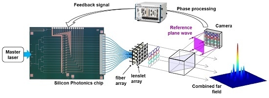
In the following we present, in detail, the workflow of the silicon photonic chip for the coherent beam combining application which is a key application driver in the PLAT4M project. We present each critical stage of the development chain: motivation for the application, photonic chip design and fabrication, photonic packaging, test and characterisation.
Coherent beam combining (CBC) of fibre lasers provides an attractive mean of reaching high output laser power by scaling up the available energy while keeping fibre intrinsic advantages of compactness, reliability, efficiency, and beam quality. In CBC architectures, the power of a master oscillator (MO) is divided into N fibres that are amplified individually. The N amplified output beams are then combined coherently in order to produce ideally an optical beam with a brightness increased by N with respect to the individual beams. Moreover, this laser architecture provides a synthetic aperture with phase front control ability which permits output beam steering and atmospheric phase perturbation compensation.
The coherent addition means that the optical phases of all the channels are locked, either in a passive way [
1,
2] or, using active phase lock loops (PLLs) [
3,
4,
5]. This last approach, we chose for this work, is commonly preferred when a large number of fibres are considered (typically above 10 to 20). Then, as many PLLs as the number of fibres have to be implemented, which underlines the need for collective technologies and methods. First prerequisite for a PLL is to measure the phase perturbation between the propagation channels. This can be done using various techniques [
3,
4,
5], among which we chose an interferometric approach, which has the advantages of being collective and scalable to potentially very high number of fibres (up to hundreds) [
5].
An important part of the system is the fibre channel preparation, i.e., the splitting of the incident master oscillator into N channels, and the addition of one phase modulator per channel, required to feed back the system and close the PLLs. For this particular purpose, Silicon Photonics technology can bring unique advantages for these splitting and phase modulation functionalities. When a potentially very large number of channels is envisaged, volume and cost considerations become critical, and an integrated solution, carrying these functionalities on a single or few chips, is mandatory for an economically viable system. Our demonstrator aims at validating the integration of Silicon photonic functions for channel splitting and phase modulators arrays in a passive CBC experiment.
3. Photonic Packaging
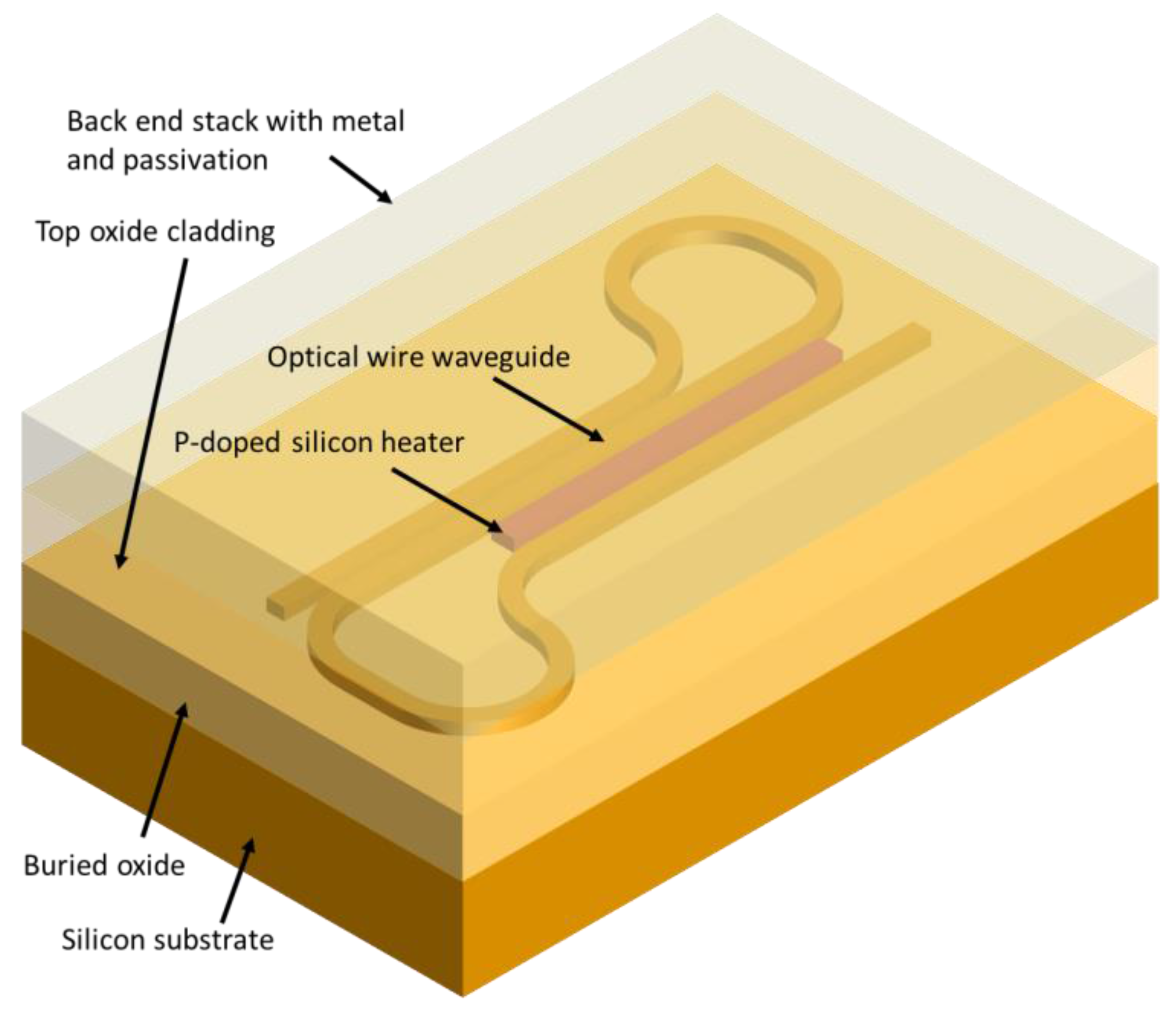
The photonic chip is housed onto a custom test board that allows us to connect the 16 heaters to a DC connector. A 10 kΩ thermistor is placed in good thermal contact with the IC. The printed circuit board (PCB) presents thermal vias on the PIC footprint, and a thermoelectric cooler is mounted underneath the PCB for temperature control of the device. The test-unit is assembled on top of an optical breadboard that acts also as heat-sink for the thermoelectric cooler (TEC).
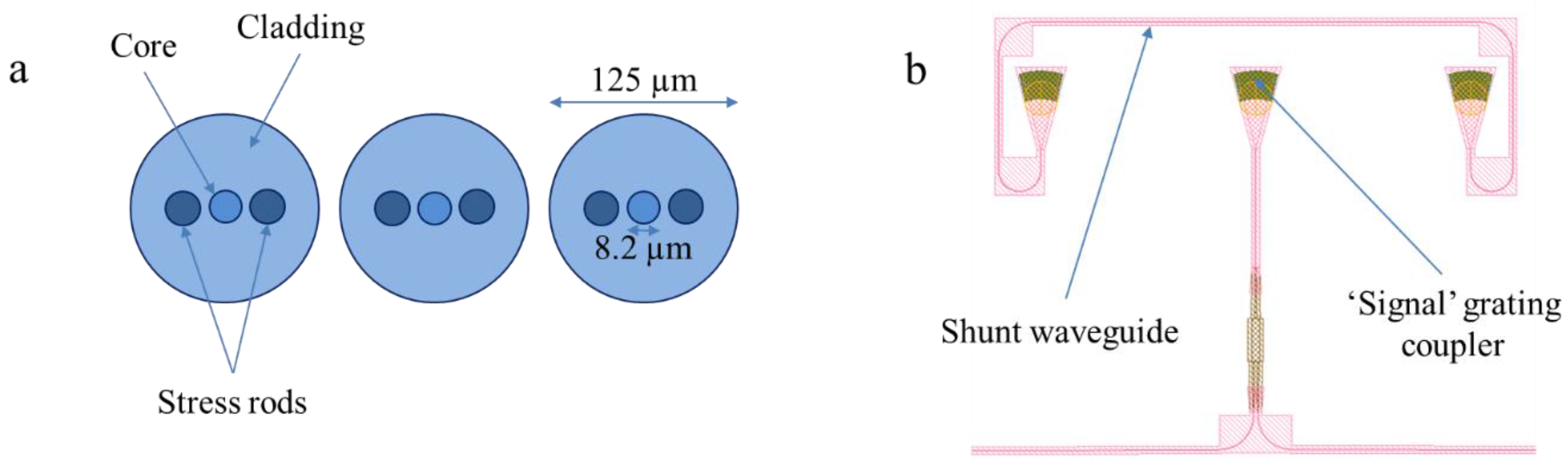
The cross-section of single mode Si photonics waveguides @ 1550 nm is 220 nm × 450 nm. Diffracting grating couplers [
7] are used for optical coupling between waveguides and single-mode fibres. For Coherent Beam Combining, it is necessary to use polarization maintaining (PM) fibres to connect to the Silicon waveguides. The 1D grating couplers implemented on this demonstrator support only transverse-electric (TE) polarization of light. The fibre stress rod orientation shown in
Figure 3a allows only the TE mode to reach the grating couplers. Active alignment is required for optical coupling between single-mode fibres and PIC [
11]. We use two extra grating couplers or “optical shunts” in addition to those on the input signal channels,
Figure 3b. These shunts are necessary for accurate fibre alignment and they avoid the need to use the signal channels during the alignment process. The active alignment process involves maximizing the signal coupled into the shunt waveguide when the fibre array is scanning in a near contact position to the Si-PIC surface.
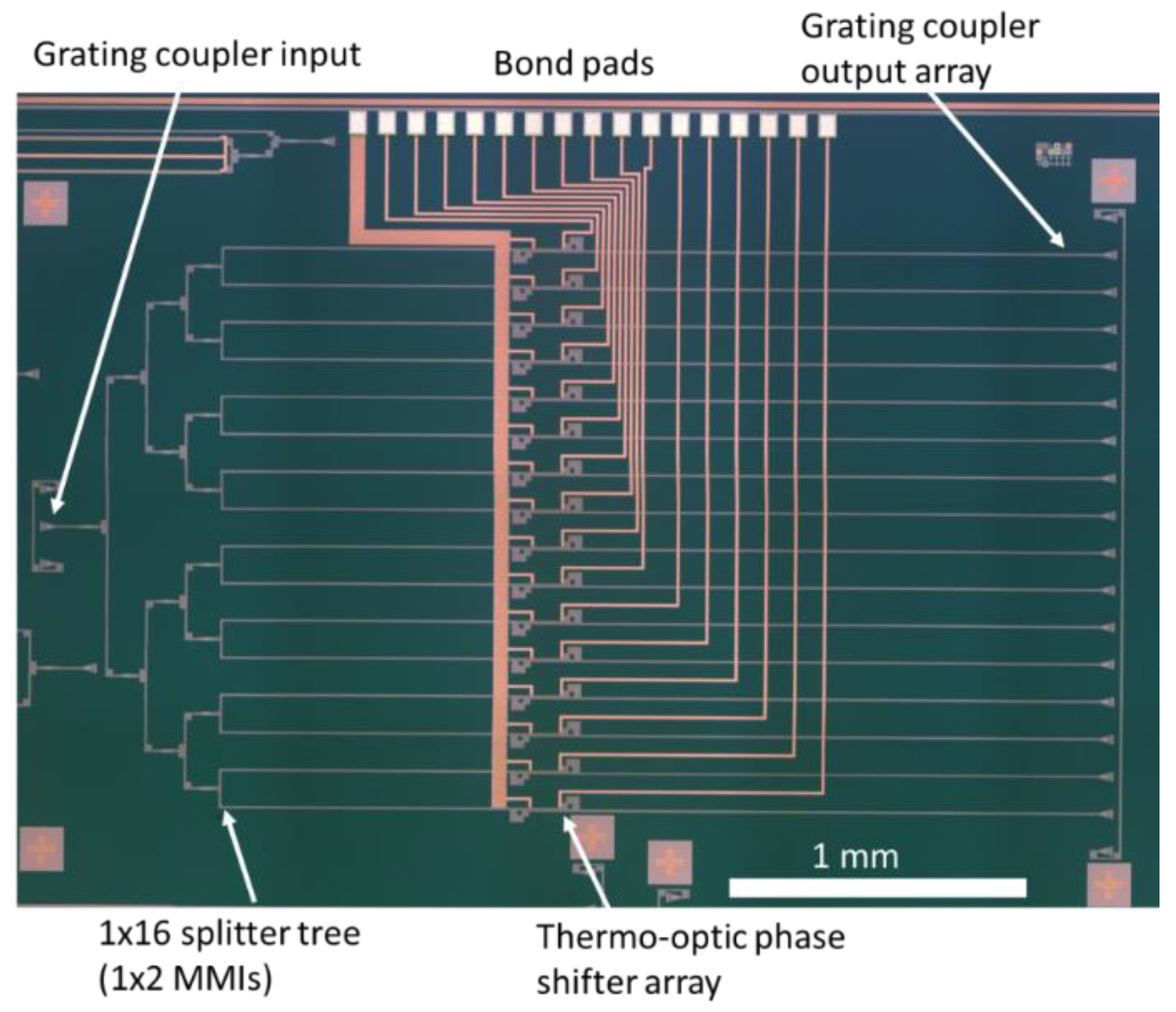
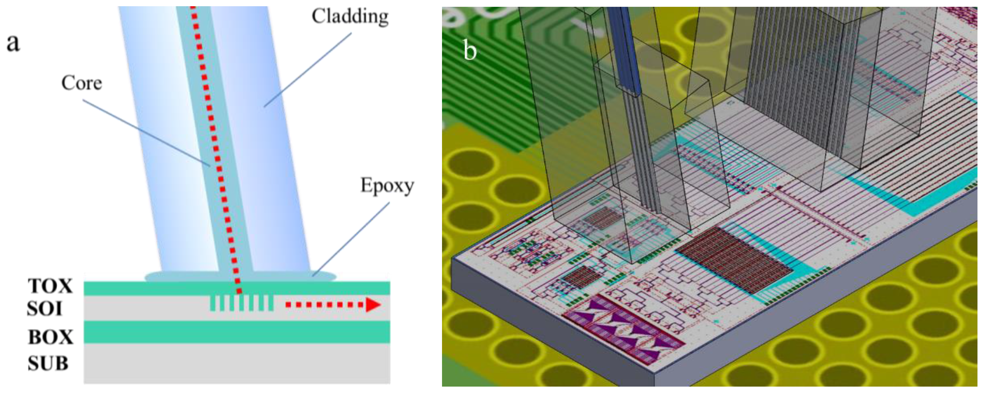
Figure 2.
Microscope image of the demonstrator circuit after finalizing the silicon Photonic Integrated Circuit (PIC) fabrication process.
Figure 2.
Microscope image of the demonstrator circuit after finalizing the silicon Photonic Integrated Circuit (PIC) fabrication process.
Figure 3.
(a) Polarization maintaining fibre array with stress rods oriented to deliver transverse-electric (TE) mode on the grating couplers; (b) Shunt waveguide connecting two dummy grating couplers for active fibre coupling process.
Figure 3.
(a) Polarization maintaining fibre array with stress rods oriented to deliver transverse-electric (TE) mode on the grating couplers; (b) Shunt waveguide connecting two dummy grating couplers for active fibre coupling process.
Grating couplers designed for this application require light incident at 10° off-vertical and the channel pitch is 127 µm, corresponding to standard fibre arrays. When the fibre array is positioned on the maximum coupling efficiency point through the shunt waveguide, a thin layer of low-shrinkage UV cure epoxy is used to bond the fibre block onto the PIC surface, see
Figure 4a. The epoxy refractive index (
n) is approximately 1.5, which is close to the refractive indices of the fibre and the SiO
2 cover layer on top of the grating coupler.
Figure 4b shows the 3D model of the fibre connection to the PIC. Two different fibre arrays have been used for the input and the 16 outputs. On both sides, two grating couplers shorted by a waveguide enable the active alignment of the fibres.
Figure 4.
(a) Fibre connection to the grating coupler. The fibre block is polished at 10° and a thin layer of “optical” epoxy is used to bond the fibre onto the photonic chip; (b) 3D model of the fibre connection to the PIC. The PIC presents one input and 16 outputs. On both input and output side two additional grating couplers have been added to support the active fibre alignment.
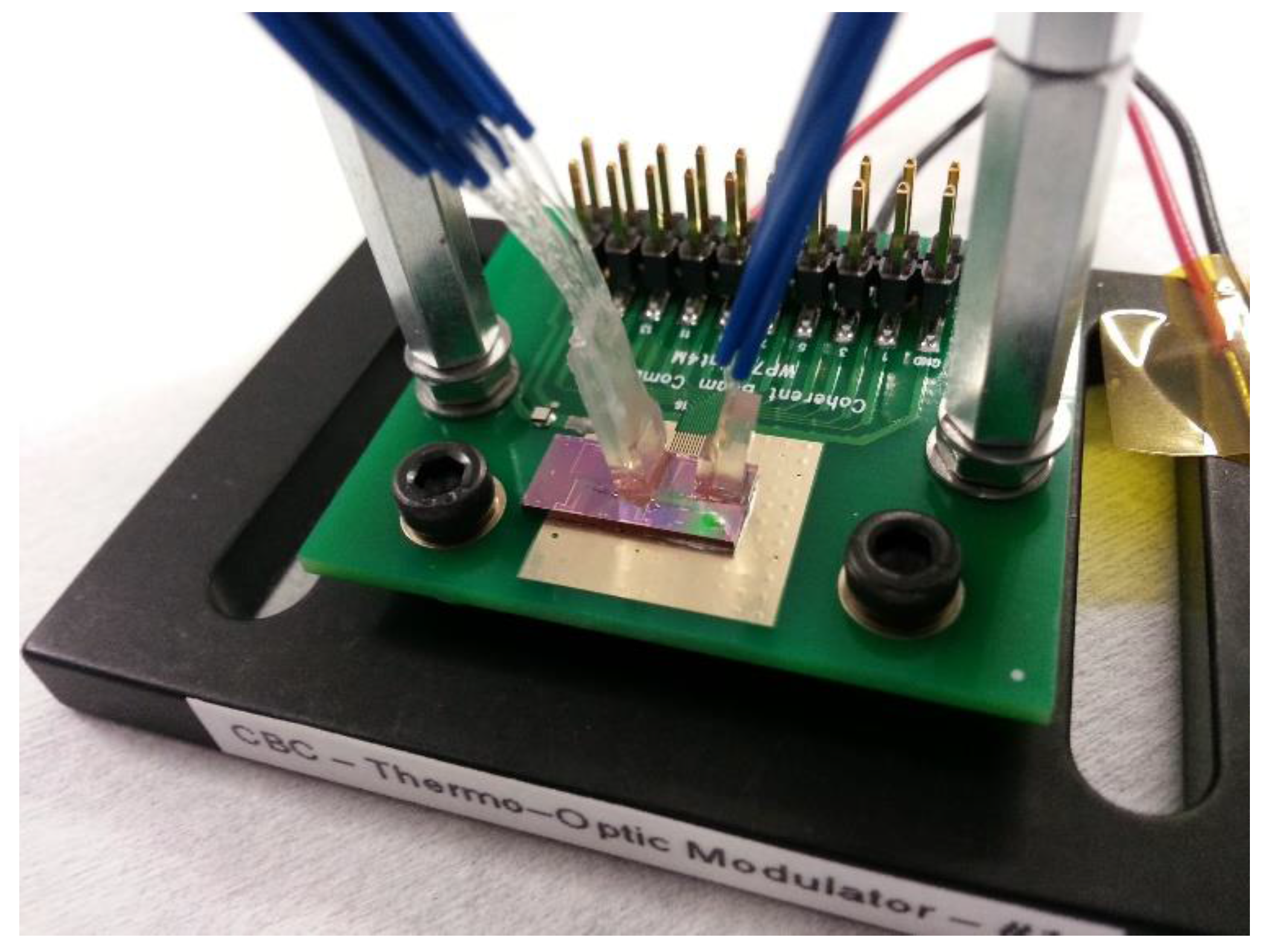
Figure 5 shows a completed prototype, note the two posts supporting the bulky fibre bundle to avoid unnecessary stress on the joint between fibre array and PIC. It should be noted that it is possible to use a planar fibre array for a more compact overall assembly [
11]. However, this initial CBC prototype used the vertical fibre design. As mentioned previously, this prototype includes 16 channels, which is still far from the hundreds or more potentially required for extremely high power CBC sources. The main challenge for scaling up this channel count is on the packaging side. With the current fibre coupling approach, the chip area increases linearly with the number of channels, with huge impact on the cost. However, 2D fibre arrays should be a valuable implementation in the future, to scale up to tens of channels on a chip with moderate dimensions.
Figure 5.
Photo of the coherent beam combining (CBC) prototype. The Si-PIC is housed onto a custom printed circuit board (PCB) and two fibre arrays are aligned and attached on top of the Photonic Integrated Circuit (PIC) using ultraviolet cure epoxy.
Figure 5.
Photo of the coherent beam combining (CBC) prototype. The Si-PIC is housed onto a custom printed circuit board (PCB) and two fibre arrays are aligned and attached on top of the Photonic Integrated Circuit (PIC) using ultraviolet cure epoxy.
Although the chip fabrication process is ready for large scale production, the packaging process is based on active alignment and not yet suitable for high volume manufacturing. This lack on the packaging side will be soon addressed by industry using vision based optical coupling techniques.
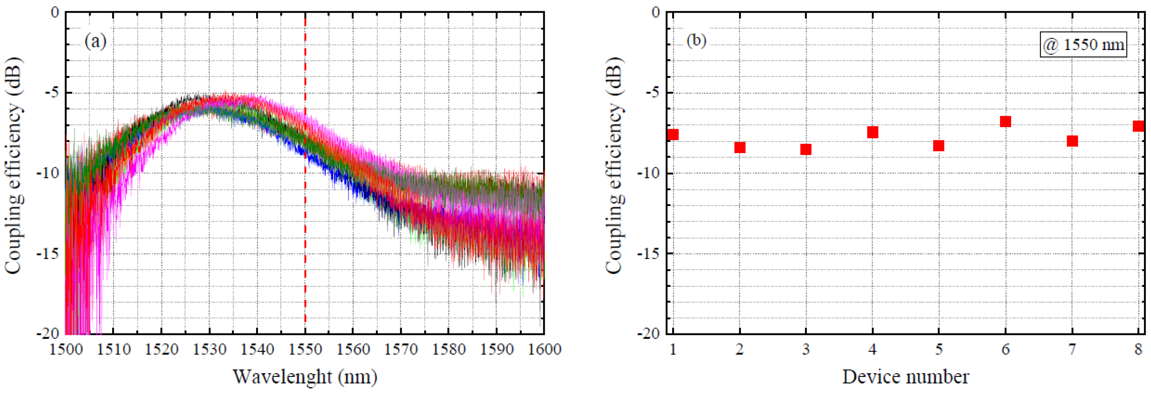
Figure 6a shows the wavelength response across the shunt waveguide for the four demonstrators prepared. It is peaking at 1535 nm. At 1550 nm, the CBC operation wavelength, the insertion loss for each grating coupler is 4 dB with less than 1 dB fluctuation, see
Figure 6b. It represents also the insertion loss of the device in each channel (excluding the 1:16 splitter block). The grating couplers are designed to peak at 1550 nm with a “fibre-air-chip” interface when flat-end fibres at 10° off-vertical are used for optical coupling. This interface is not present in the packaged device because index matching epoxy is used to bond the fibres onto the chip. As a result there is not refraction at the silicon oxide interface and the beam shines the grating coupler with a different angle resulting in a shift of the peak wavelength.
Figure 6.
(a) Grating coupler wavelength response on the eight measured samples. The coupling efficiency peaks at 1535 nm and is still acceptable at 1550 nm; (b) Coupling efficiency at 1550 nm of the eight tested structures. The insertion loss on each grating coupler is of about 4 dB and the uniformity is better than 1 dB.
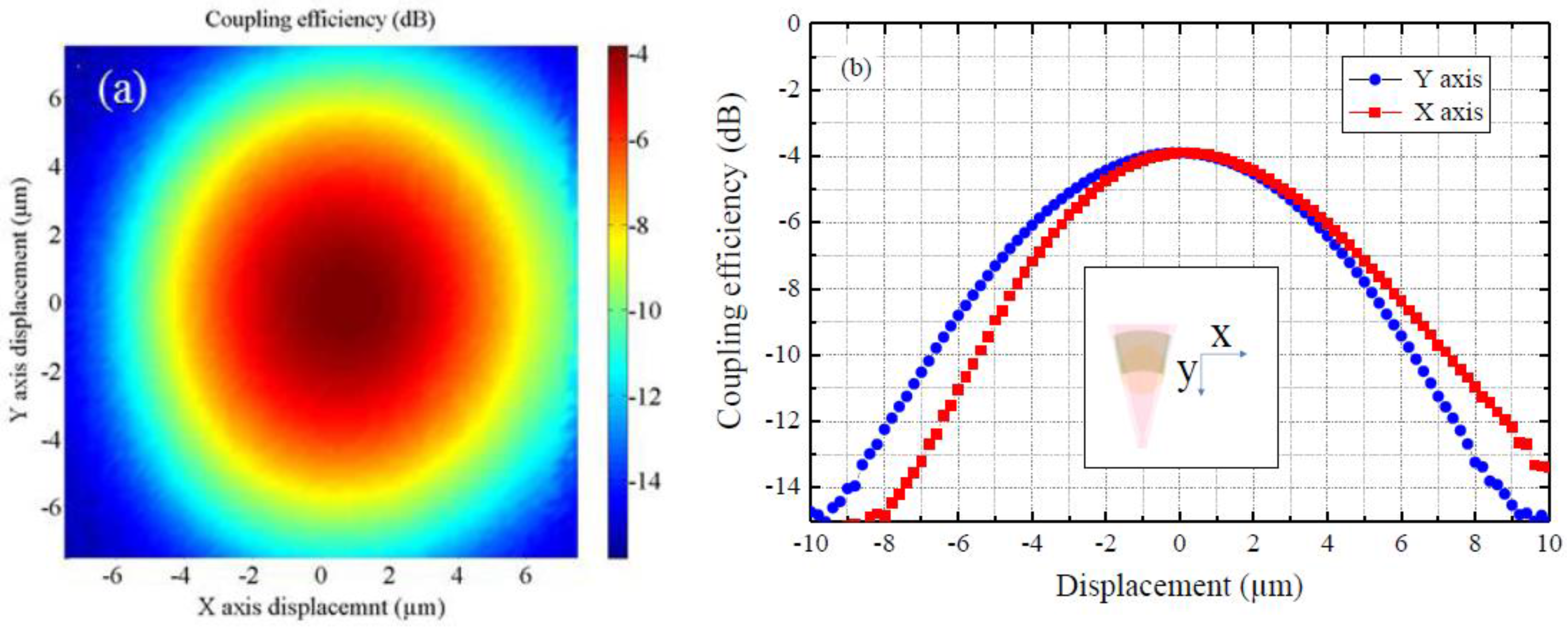
We also investigated the alignment tolerance of our grating couplers using standard single-mode fibres (SMF-28), see
Figure 7. The coupling efficiency through the shunt waveguide was recorded while the fibre array was swept over the grating coupler with a 200 nm step. The alignment tolerances results are relatively relaxed: about 1 dB of additional losses over a planar misalignment of ± 2.5 µm, which is in good agreement with values reported in literature [
12].
Figure 7a shows the 2D map of the grating coupler alignment tolerances over an area 15 µm × 15 µm.
Figure 7b shows the grating coupler efficiency recorded moving the fibre along two orthogonal axes on the grating plane.
Figure 7.
(a) Grating coupler alignment tolerance measurement; (b) X and Y scan of the fibre on the grating coupler plane showing about 1 dB of extra insertion losses with a fibre displacement of ± 2.5 µm.
Figure 7.
(a) Grating coupler alignment tolerance measurement; (b) X and Y scan of the fibre on the grating coupler plane showing about 1 dB of extra insertion losses with a fibre displacement of ± 2.5 µm.
5. Results and Discussion
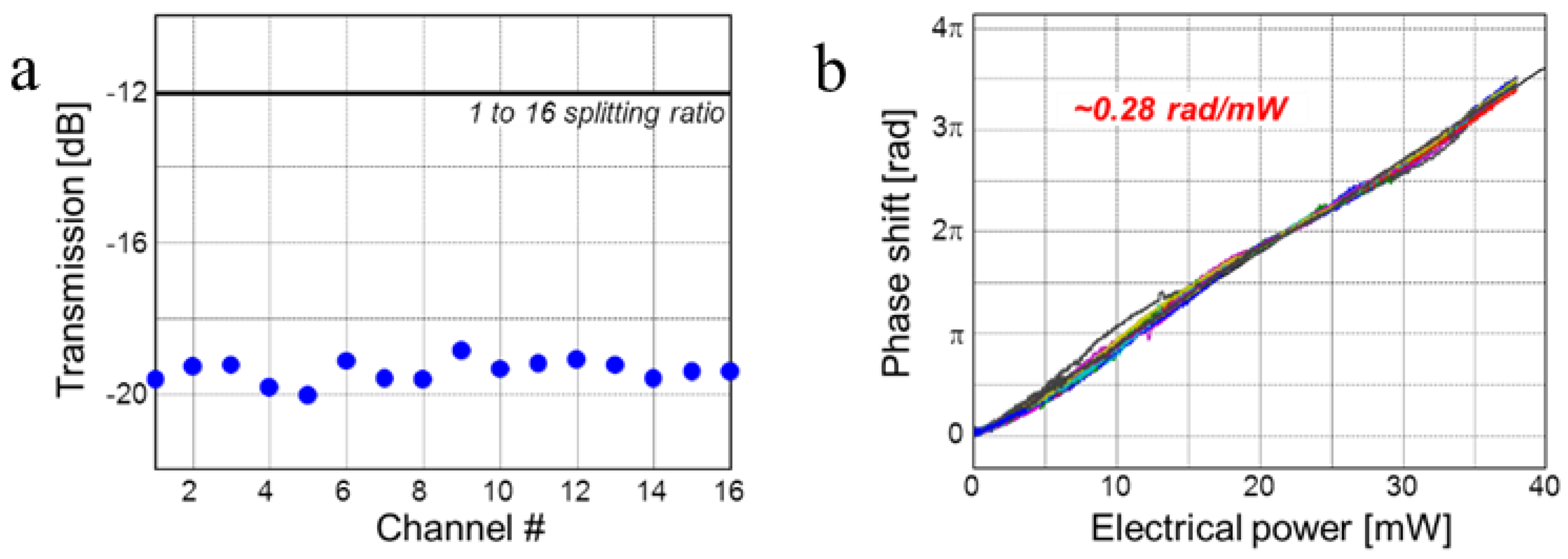
The fibre-to-fibre transmission measurement is shown in
Figure 9a. The overall insertion loss homogeneity is about 1 dB, and the insertion loss of the device is 7 dB per channel, excluding the 1:16 ratio of the splitter tree. The phase responses of the PIC’s modulators are collectively measured using our CBC interferometric set up, by applying square shaped voltage waveforms at 1 kHz frequency to the modulators. Therefore, we make sure that the thermal modulator technology is suitable with our chosen 1 kHz loop frequency for the PLLs. As shown in
Figure 9b, the phase responses of all the 16 channels are very homogeneous, with a slope efficiency of 0.285 rad/mW. Therefore, a 2π phase shift is achieved for 22 mW of electrical driving power.
Figure 9.
(a) Fibre-to-fibre transmission of the 16 channels; (b) Phase modulation response for the 16 channels (superposed colored lines).
Figure 9.
(a) Fibre-to-fibre transmission of the 16 channels; (b) Phase modulation response for the 16 channels (superposed colored lines).
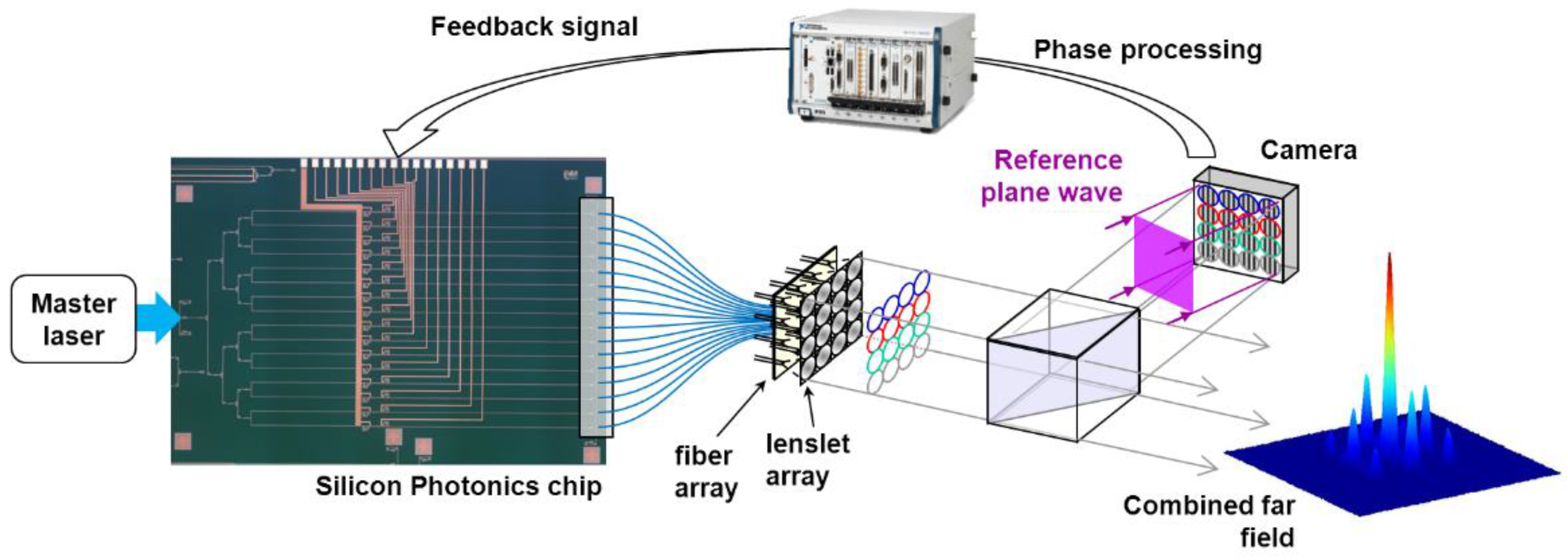
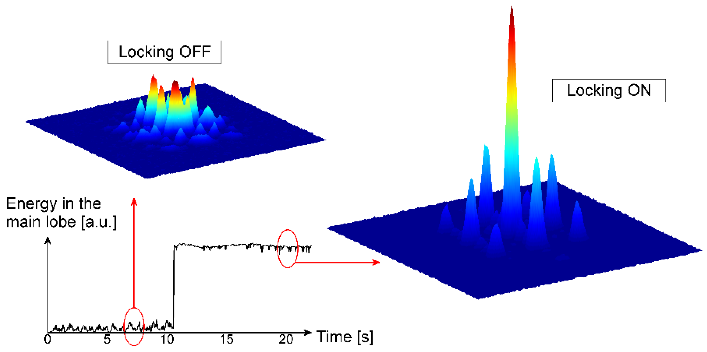
Finally, the successful coherent combination is evidenced by recording the far field of the 16 parallel and collimated output beams. As shown in
Figure 10, when the PLLs are off, the far field pattern is a fluctuating speckle-like profile resulting from the interference of the 16 beams with random phase distribution. When the PLLs are on, the phases of all the 16 channels are locked together and form an overall plane phase front for the composite output pupil of the system. This result in the far field pattern is shown in
Figure 10 (right), with a bright and stable central lobe. The intensity lost here in the satellite lobes is just a result of the filling factor of the individual beams in the collimating microlenses plane. The temporal stability of the system is also illustrated in the plot below, with the energy encircled in the main central lobe plotted against time. The measured channel-to-channel residual phase error in closed loop configuration is below λ/120.
Figure 10.
Experimental far field pattern of the 16 combined beams, when PLLs are off (upper left), and when PLLs are on (right). The plot shows the temporal evolution of the energy encircled in the main central lobe of the combined beam.
Figure 10.
Experimental far field pattern of the 16 combined beams, when PLLs are off (upper left), and when PLLs are on (right). The plot shows the temporal evolution of the energy encircled in the main central lobe of the combined beam.
The optical power incident on the chip here was 10 dBm, meaning approximately −9 dBm at each fibre output. This is still too low for a real system application where fibre amplifiers have to operate in saturation regime. The next generation of devices will be able to handle one to two orders of magnitude higher input power.
6. Conclusions
The growing interest in Silicon photonics is mainly driven by its ability to satisfy demands in large markets, particularly for datacoms, medical diagnostics and sensing applications. Device fabrication based on CMOS wafer-scale processes can meet this demand. However, device fabrication is only one element of the supply chain necessary to produce fully working sub-systems. In this paper, we have shown how the PLAT4M project is addressing this technological supply chain challenge, by bringing together a range of capabilities from around Europe, from Si-PIC design, through to device fabrication, packaging and final test. We reported the demonstration of this full supply chain through one of the applications developed in PLAT4M, a Si-PIC Coherent Beam Combiner. It is however worthwhile mentioning that the PLAT4M supply chain is also used in the project for the development of other applications, namely laser Doppler vibrometry, gas sensing and a Datacom transceiver compatible with the 100GBase-LR4 standard. A key feature of this collaboration is the need for each partner to understand and to account for other elements in the supply chain. For example, device designers need to account for packaging when preparing chip layout, ensuring factors such as grating coupler pitch and shunt waveguides are included to ease the fibre alignment process. The PLAT4M project highlights the need for a consortium-driven approach to integrated photonics, where all elements of the technology supply chain work together to achieve a single objective.


