1. Introduction
Light trapping via the chemical and geometric design of solar cells promises to dramatically increase solar cell efficiency by increasing light absorption without increasing the exciton or free carrier collection length. Various approaches have been proposed to enhance the overall solar cell efficiency in the thin film or nano-based solar cells. These include: putting a photonic crystal or distributed Bragg reflector in the back of thin film solar cells [
1,
2,
3], using a disperse carbon interlayer and textured photonic crystal backside reflector to prompt back reflected effects [
4,
5], and combining holey double-layer photonic crystals with ultrathin c-Si solar cells [
6]. Recently, solar cells utilizing nanowire arrays, overlapping nanospheres, nano-colloids, and self-assembled silver nanoparticles have shown promise by exhibiting enhanced light trapping effect and greater energy absorption rates than conventional planar semiconductors [
7,
8,
9,
10]. Grandidier
et al. [
8] experimentally and theoretically demonstrated efficiency enhancements in solar cells from dielectric nanosphere arrays. Mendes
et al. [
9] developed novel plasmonic back-reflector structures using spherical gold colloids for pronounced far-field scattering with a remarkable broadband enhancement. Morawiec
et al. [
10] demonstrated the broadband absorption enhancement of thin solar cells due to the light scattering effects of plasmonic back reflectors composed of self-assembled silver nanoparticles. Specifically, nanowire arrays have drawn a great deal of attentions due to their optical absorption properties which can enhance the light trapping effect. Hu and Chen [
11] demonstrated that Si nanowire is capable of significantly improving light absorption when compared to a typical Si thin film within a high frequency region. ZnO has also been studied extensively as a semiconductor in solar cell applications due to its wide band gap and high electron mobility [
7,
12,
13]. Ordered arrays of nanowires can benefit from diffraction effects, collective resonances, and changes in the optical density of states which are absent in single nanowire or random arrays of nanowires. Garnett and Yang [
14] measured the photocurrent of solar cells made with ordered silicon nanowire arrays with different silicon absorber thicknesses to determine the light trapping path length enhancement factor. The current study of nanowire arrays has been focused mainly on Si and ZnO type compositions. Myung
et al. [
15] synthesized a high density ZnO/CdS core-shell nanowire array by depositing the CdS outer layers on pre-grown, vertically-aligned ZnO nanowire, through chemical vapor deposition. Seol
et al. [
16] created a CdSe/CdS/ZnO nanowire array through a three-step solution-based method which was used as a photoanode of a quantum dot sensitized solar cell capable of generating a maximum power conversion efficiency of 4.15%. Although experimental observations of the enhanced absorptions have been reported in those solar cells with nanowire arrays, few theoretical and simulation works have been conducted which can be very useful to provide guidelines for designing high efficiency solar cell plates with outstanding light trapping effect.
Moreover, photonic nanowire arrays assembled with thin film structures have exhibited an increase in light trapping in a large frequency range. Li
et al. [
17] found that optical absorption can be greatly enhanced with the addition of a Si nano-pillar to a Si thin film owing to suppressed reflection and transmission. Lin
et al. [
18] demonstrated an improvement in the photovoltaic performance of a ZnO/P
3HT hybrid nanostructure through interface molecular modification on the ZnO nanowire surface. Wu
et al. [
19] reported a 74% increase in efficiency of ZnO nanowire dye-sensitized (DSSC) thin film solar cells. Mokkapati
et al. [
20] provided criteria for optimizing light trapping of metal nanoparticles in periodic arrays in a long wavelength range, allowing for a higher order diffraction mode while maintaining the highest possible fill factor. Therefore, designing a photonic crystal unit cell that combines multilayer thin film structures and multi-shell nanowires with optimized geometric properties can lead to solar cells with a broadband, high-energy absorption rate.
The objective for this paper is to investigate a solar cell consisting of multilayer thin film structures, as well as periodic core-shell nanowire photonic crystals, as an optical absorber. First, theoretical and numerical analyses are carried out on a simple five-layered thin film solar cell. Next, a microstructural design consisting of ZnO/CdS nanowire arrays and multilayer thin films is proposed. Light absorbing performance of the proposed design is evaluated numerically. In order to yield the highest absorption rate possible in both low and high frequency ranges, non-linear optimization is carried out to generate structural geometries that exhibit excellent absorption performance in a broad frequency range.
2. Theoretical Analysis of One-Dimensional Solar Cell with Multilayer Nano Films
To achieve broadband optical absorption in real structures such as thin solar cell plates, photonic nanostructures designed with complex geometries are considered. Theoretical investigation of multilayer nanoscale thin film inside the solar cell plate can be a good starting point to understand the energy absorption inside the solar cell nanostructures. In addition, the periodicity of the solar cell nanostructures can be designed along with the reflection and transmission rates. Furthermore, numerical simulations should be performed to yield the optimal structural parameters and, therefore, increase the photon absorption rate.
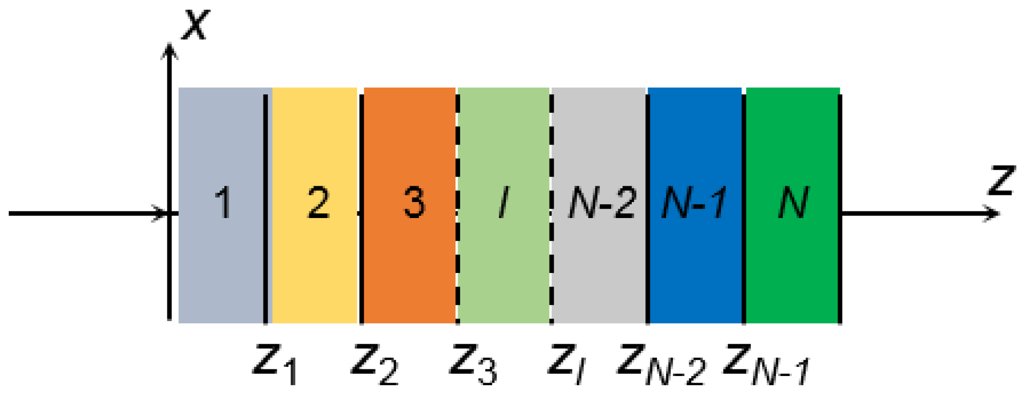
First, theoretical investigations of the one-dimensional (1D) multilayer solar cell plate are conducted, with the goal of achieving a guideline for the microstructural design that is focused on absorption in a high frequency region. This model will then be extended to the three-dimensional (3D) case in the next section to investigate and design a solar cell with both nanowire arrays and composite thin films. In order to understand the underlying physical mechanism for photon absorption in optical resonance, analytical modeling as well as numerical simulations are carried out. An analytical model of the multilayer planar solar cell is initially constructed by using the matrix transfer formulation to calculate the reflection and transmission in a 1D multilayered planar structure, as shown in
Figure 1. The structure consists of (
N – 2) layers sandwiched together by two semi-infinite layers (layer 1 and layer
N).
Figure 1.
1D multilayer planar structure.
Figure 1.
1D multilayer planar structure.
The relative permittivity, permeability, and refractive index of the
l-th layer is denoted by
ɛl,
µl and
nl (
l = 1, 2,…,
N), respectively. Each layer of the multilayer structure is a medium with complex permittivity and magnetic permeability given by [
21]:
where the imaginary portion represents optical absorption behavior in the medium and the dielectric loss tangent can be written as:
In this paper, we use relative permittivity when carrying out analysis and simulations, which is defined as the ratio of dielectric permittivity over the permittivity of vacuum. For the transverse electric (TE) wave, the electric and magnetic fields in the region
l are given by [
22]:
where
z0 =
zl = 0,
zl =
zl−1 +
dl and
dl is the thickness of the
l-th layer (
l = 2,…,
N − 1). The constants
Al and
Bl represent wave components with the propagating velocity components along the positive and negative
z directions, respectively. The variables
ɛ0 and
µl are the permittivity and permeability of vacuum, respectively. The total fields for transverse magnetic (TM) waves can then be obtained by interchanging
,
, and
in Equation (3). The constants
Al and
Bl can be determined by using interfacial conditions at
(
l = 1, 2,…,
N − 1), which lead to:
where
is the inverse matrix of
. The matrices
and
are given by
respectively. In Equations (5) and (6),
and
with
for a TE wave and
for a TM wave. Note that
where
nl2 =
ɛl (
l = 1, 2,…,
N − 1) is the refraction index. From Equation (4), we can derive the following relation
where the 2×2 matrix
.
One can set
BN = 0, since there is no reflection in the region
N. Therefore, the transmission and reflection coefficients can be calculated as
and
, respectively.
(
i,
j =1, 2) are the components of the 2 × 2 matrix
M. Finally, the power transmittance
T and reflectance
R can be calculated as:
respectively, where
.
Figure 2.
Five-layer thin film solar cell under different angles of incidence.
Figure 2.
Five-layer thin film solar cell under different angles of incidence.
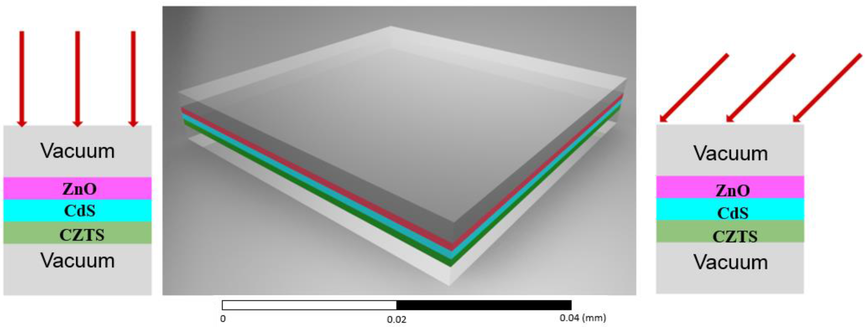
In
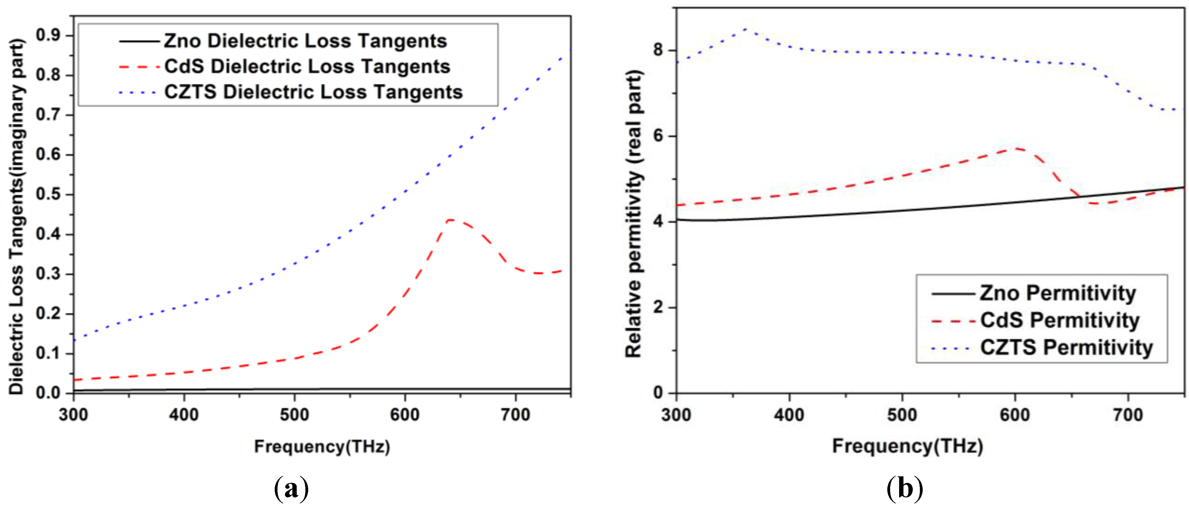
Figure 2, a five-layer thin film solar cell with vacuums as the top and bottom outer layers are studied with different angles of incidence. Both a theoretical model and finite element (FE) model are used to calculate the reflection, transmission, and absorption rates of the five-layer thin film. The relative permittivity and dielectric loss tangents of ZnO, CdS, and CZTS layers are all frequency-dependent and determined through experimental measurement.
Figure 3a,b demonstrate the dielectric loss tangents and the real parts of the relative permittivity of the three layers, respectively.
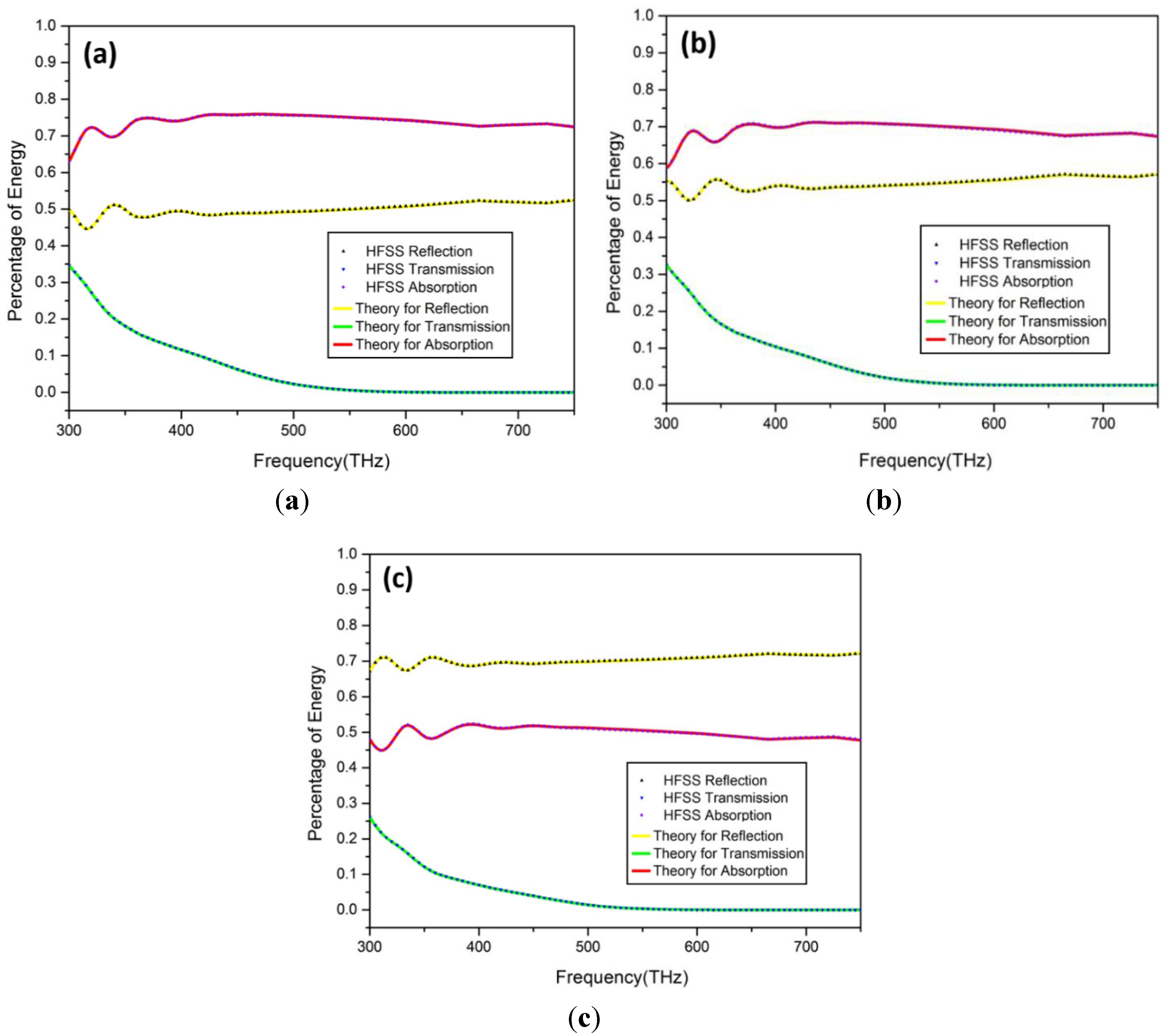
The thicknesses of ZnO, CdS, and CZTS layers are 400, 200 and 200 nm, respectively. Three different angles of incidence (0°, 30°, and 60°) are studied. In order to validate the analytical model, a numerical simulation is also conducted on the five-layer thin film with the same dispersive material parameters by using Ansoft HFSS14. In
Figure 4, the reflection, transmission, and absorption results obtained from the theoretical model and the FE model are plotted as solid curves and small triangles, respectively. Excellent agreement between the two results can be observed, which confirms that the developed theoretical model can describe the exact wave behavior in the multilayer thin film solar cell.
Figure 3.
(a) Imaginary parts of the dielectric loss tangent. (b) Real parts of the relative permittivity of ZnO, CdS, and CZTS layers.
Figure 3.
(a) Imaginary parts of the dielectric loss tangent. (b) Real parts of the relative permittivity of ZnO, CdS, and CZTS layers.
Figure 4.
Theoretical and numerical results of the reflection, transmission and absorption of the five-layer thin film solar cell under (a) 0°. (b) 30°. (c) 60° angle of incident.
Figure 4.
Theoretical and numerical results of the reflection, transmission and absorption of the five-layer thin film solar cell under (a) 0°. (b) 30°. (c) 60° angle of incident.
Also, by comparing the results of the three different angles of incidence, it can be found that the reflection increases with larger angle of incident while the few changes in transmission can be observed especially in the high frequency range. The absorptions for 0° and 30° incidences are almost the same, while decreased absorption can be found when the angle of incidence increases to 60°.
3. Numerical Simulation and Optimization on Solar Cell Consisting of Core-Shell Nanowire Arrays and Multi-Layer Thin Films
Nanowire arrays have demonstrated unusual optical absorption properties in solar cell applications. Current studies of nanowires are mostly concerned with Si and ZnO compositions. Hu and Chen’s study [
11] mentioned that nanowire arrays with moderate filling ratio could exhibit greater absorption rates and lower reflectance compared with thin films, especially in a high frequency regime. The nanostructure design is of great concern in the research and development of novel solar cell structures. For nanostructures with complex geometry, the aids of numerical methods such as the finite element method (FEM) are required. In our study, a core-shell nanowire is used in order to obtain enhanced absorption. The inner core is ZnO and the outer shell is made of CdS. The core-shell nanowire is then situated within a vacuum. Simulations are conducted by using Ansoft High Frequency Structure Simulator (HFSS) with a Floquet port feature, which is capable of modeling the oblique incidence and polarization of the wave at the boundary of the periodic-planar structure. A photonic structure is created by using MATLAB in combination with HFSS’s Visual Basic scripting. Results of the magnitude and phase of the reflected and transmitted waves, as well as absorption rate through the periodic nanostructures, are then obtained.
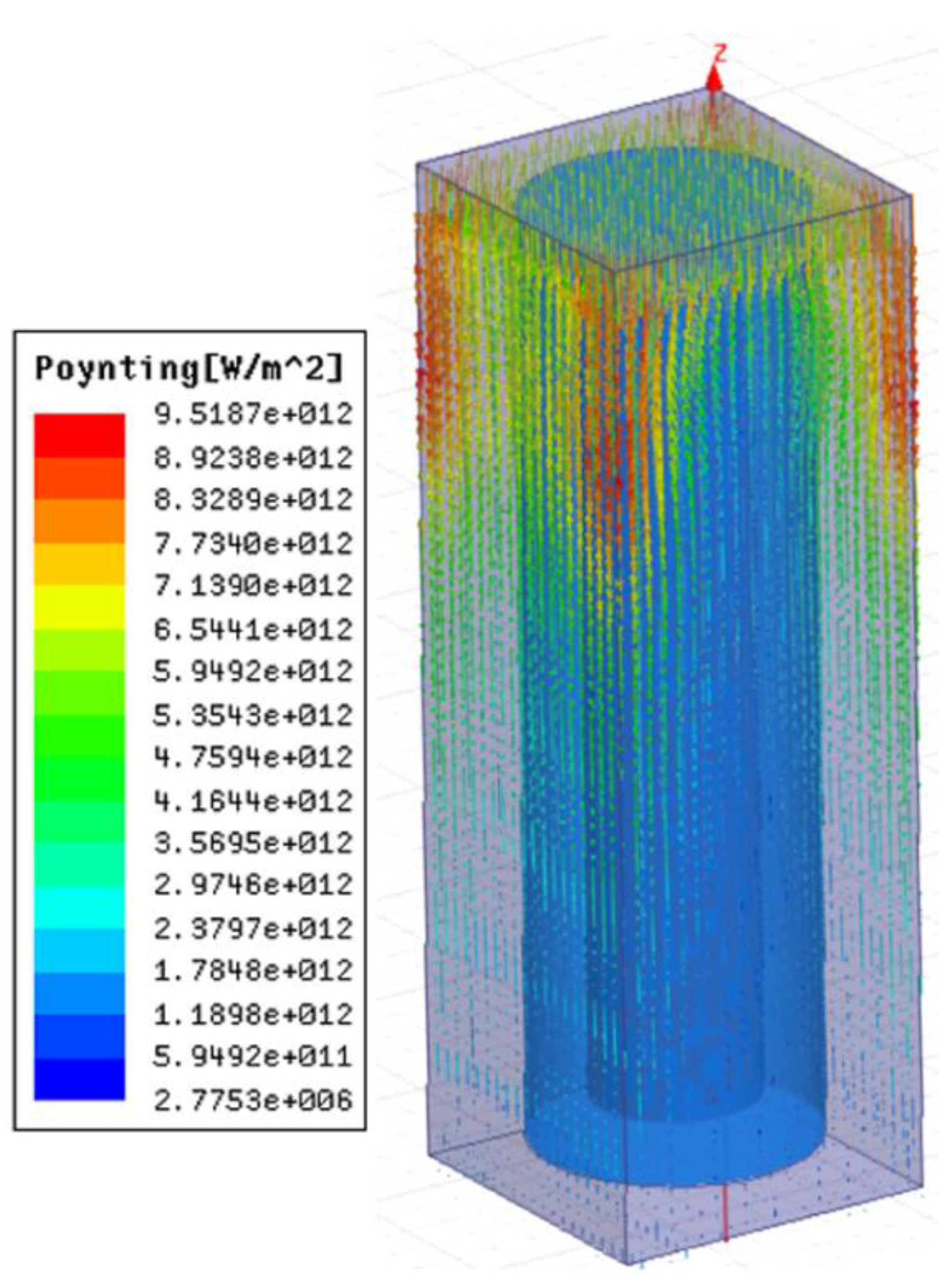
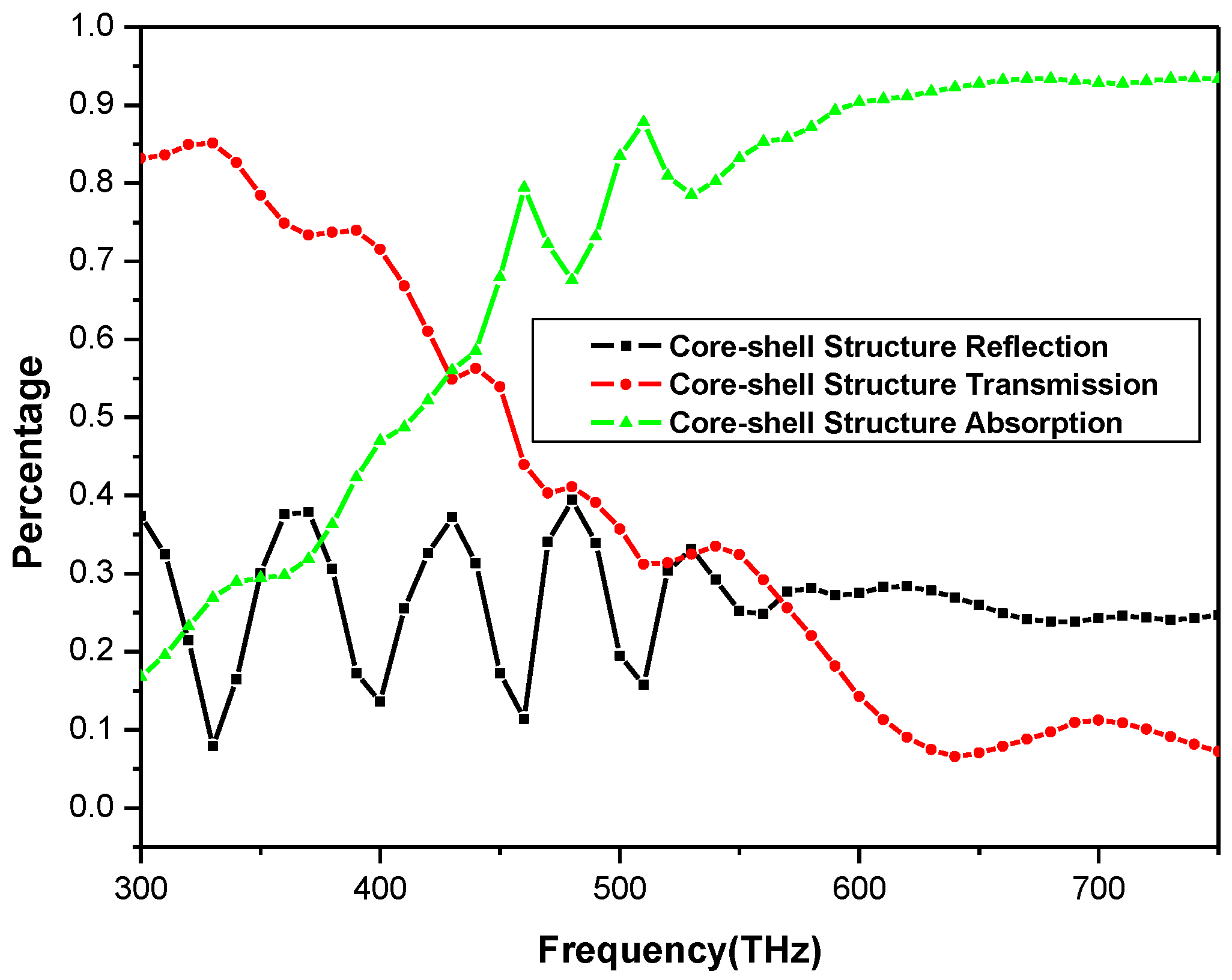
Figure 5 shows the simulation result of the energy flux density of a unit cell with core-shell nanowire structure and
Figure 6 shows the absorption rate of the core-shell nanowire structure; the coefficient describes intensity or total power percentage absorbed relative to an incident wave. In
Figure 6, we also draw the reflection and transmission coefficient curves; these two amplitude coefficients are represented by lower case r and t in Equations (11) and (12).
Figure 5.
The energy field of the unit cell with core-shell nanowire structure.
Figure 5.
The energy field of the unit cell with core-shell nanowire structure.
It can be observed from
Figure 6 that obviously higher absorption and relatively lower reflectance can be achieved at a high frequency range compared with those at a low frequency range. The influence of the optical resonance on the increased absorption can be found from 600 to 750 THz, as shown in
Figure 6. However, it will be ideal if the absorption rate is consistently high across a broad frequency range. To accomplish this, the original core-shell model needs to be modified through the optimization of structural dimensions, as well as the material compositions inside each unit cell of the nanowire array.
Figure 6.
Absorption rate of the core-shell nanowire structure.
Figure 6.
Absorption rate of the core-shell nanowire structure.
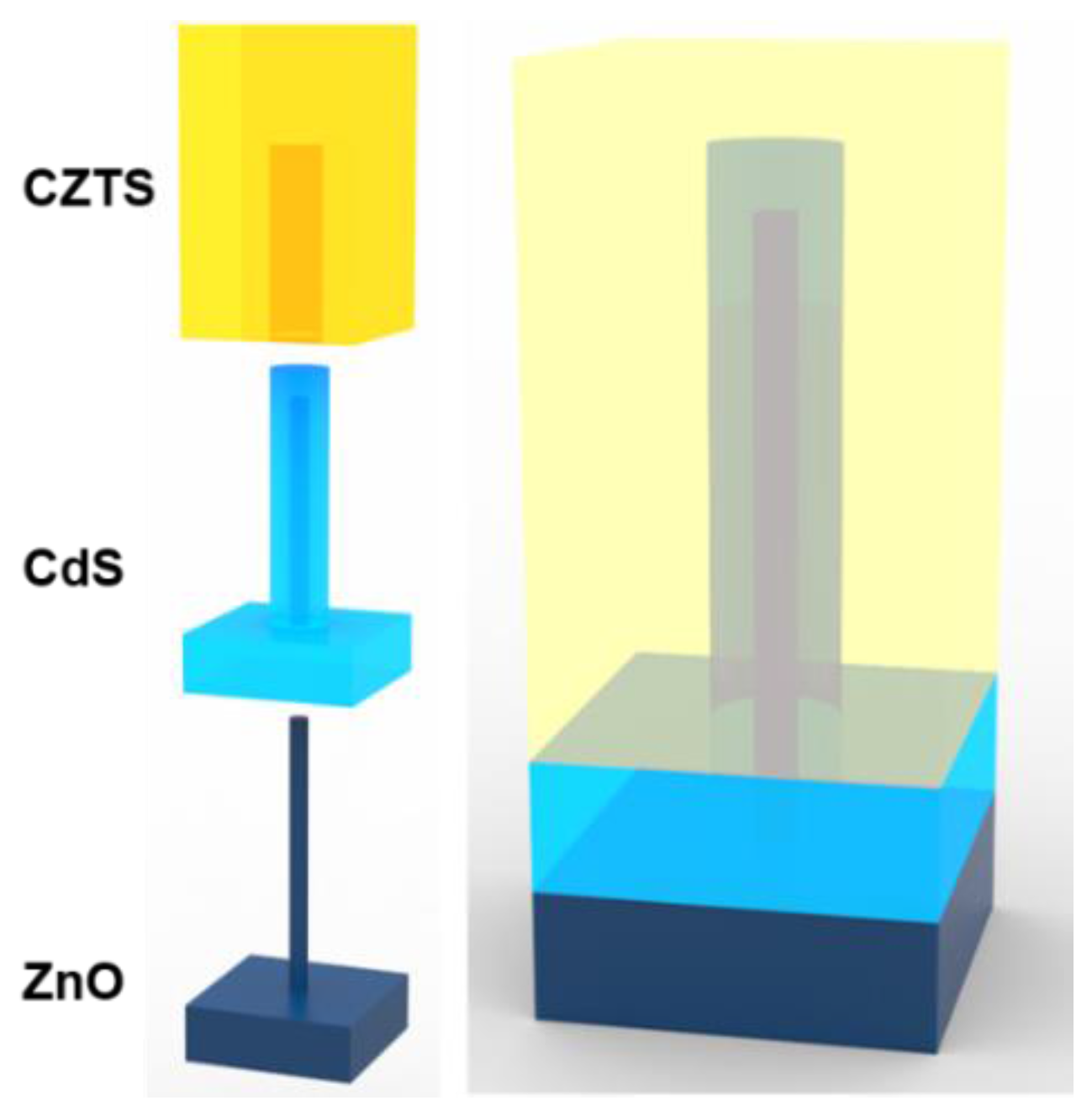
Furthermore, a nanowire array combined with a nanofilm can significantly enhance the optical absorption of a solar cell in a broad frequency range and has become a promising direction for future research of high-efficiency solar cells. By adding the Si nanowires on Si thin film, Li
et al. [
12] found that optical absorption of the combined structure could be greatly enhanced. To begin the microstructural design of the optimized 3D solar cell, we first consider a periodic array of double shelled (ZnO/CdS/CZTS) nanowire structures that are embedded in a multilayer thin film. Details of the initial unit cell design can be found in
Figure 7. A ZnO nanowire is first grown on the top of a ZnO thin film, which is then encapsulated by a layer of CdS via vapor deposition. Finally, a top layer of CZTS is added via vapor deposition to envelope the middle layer of CdS in the unit cell. Analysis on the initial design will be conducted in order to get baseline absorption rates prior to optimization.
Figure 7.
Model of the proposed nanowire-nanofilm unit cell configuration.
Figure 7.
Model of the proposed nanowire-nanofilm unit cell configuration.
The 3D solar cell is created and the optical wave simulation in the nanowire and layered medium is conducted by using Ansoft HFSS14. Periodicity of the structure is utilized in the simulation. As a result, analysis is only carried out on a single unit cell where periodic boundary conditions are applied. The Floquet port is used exclusively with planar-periodic structures in HFSS. Chief examples are planar phased arrays and frequency-selective surfaces which may be idealized as infinitely large. The analysis of the infinite structure is then accomplished by analyzing a unit cell. Linked boundaries most often form the side walls of a unit cell but, in addition, a boundary condition is required to account for the infinite space above. The Floquet port is designed for this purpose. The Floquet port is closely related to a wave port in that a set of modes (“Floquet modes”) represent the fields on the port boundary. Fundamentally, Floquet modes are plane waves with the propagation direction set by the frequency, phasing, and geometry of the periodic structure. Just like wave modes, Floquet modes also have propagation constants and experience cut-off at low frequency. Ansoft HFSS is used, of which the Floquet port can also deal with the oblique incident wave with certain polarization illuminating the periodic material structure problem. This was done in order to get the magnitude and phase of the reflection and transmission waves. The HFSS solution includes a model decomposition of which all information is obtained in the form of an S-matrix interrelating the Floquet modes.
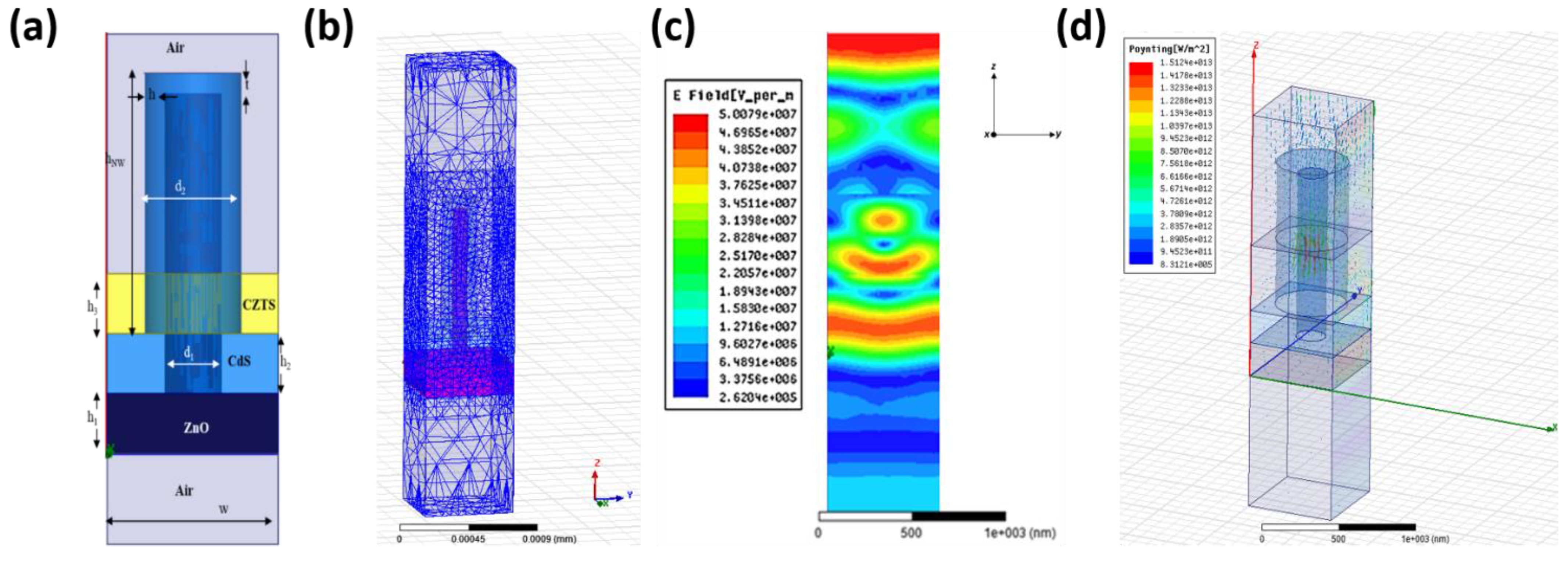
Figure 8a shows the dimensions of a single unit cell in the simulation. The three layers in the middle of the FE model are the dispersive materials CZTS, CdS, and ZnO from top to bottom, respectively. The value of permeability are all equal to unity (
µ = 1) since the materials are nonmagnetic over the entire optical frequency range of interest. The permittivity of vacuum is 1 and the others’ permittivity and dielectric loss tangents are all dispersive, experimentally-determined optical constants of those material components and are used in the FE simulation. The thicknesses of the three thin films are set to 400, 200, and 200 nm for CZTS, CdS, and ZnO, respectively. The incident light is set normal to the film substrate,
i.e., it is parallel to the nanowires. Periodic conditions are employed at a pair of surfaces parallel to the
x-z and
y-z planes by using the master/slave boundary. The final structure is realized through infinitely extending the structural units having the height of 1800 nm and a width dimension equal to the nanowire array periodicity, as indicated by the
d1 in
Figure 8a,b showing the meshed unit cell which is sandwiched between two bodies of vacuum with finite length.
Figure 8.
(a) Dimensions of a single unit cell. (b)The meshed FE model. (c) The simulated electric field flux. (d) The simulated Poynting energy field in the unit cell.
Figure 8.
(a) Dimensions of a single unit cell. (b)The meshed FE model. (c) The simulated electric field flux. (d) The simulated Poynting energy field in the unit cell.
The optical information is obtained from the spatial distribution of the electric field flux which results from the interaction between the structure and the incident light, as shown in
Figure 8c. The frequency range of the incident light varies between 300 to 750 THz corresponding to the wavelength from 400 to 1000 nm. These values are selected because they occupy the frequency spectrum of solar radiation which is of particular interest. The results of Poynting flux distribution is shown in
Figure 8d. It can be found from
Figure 8c,d that the electric field in the core-shell nanowire regime is enhanced and energy is gathered by the nanostructure due to light trapping effect. Therefore, very little energy is transmitted out, but still a large of part is reflected back by the nanostructure.
Figure 9.
FEM results for absorption rates of varies nanowire diameters.
Figure 9.
FEM results for absorption rates of varies nanowire diameters.
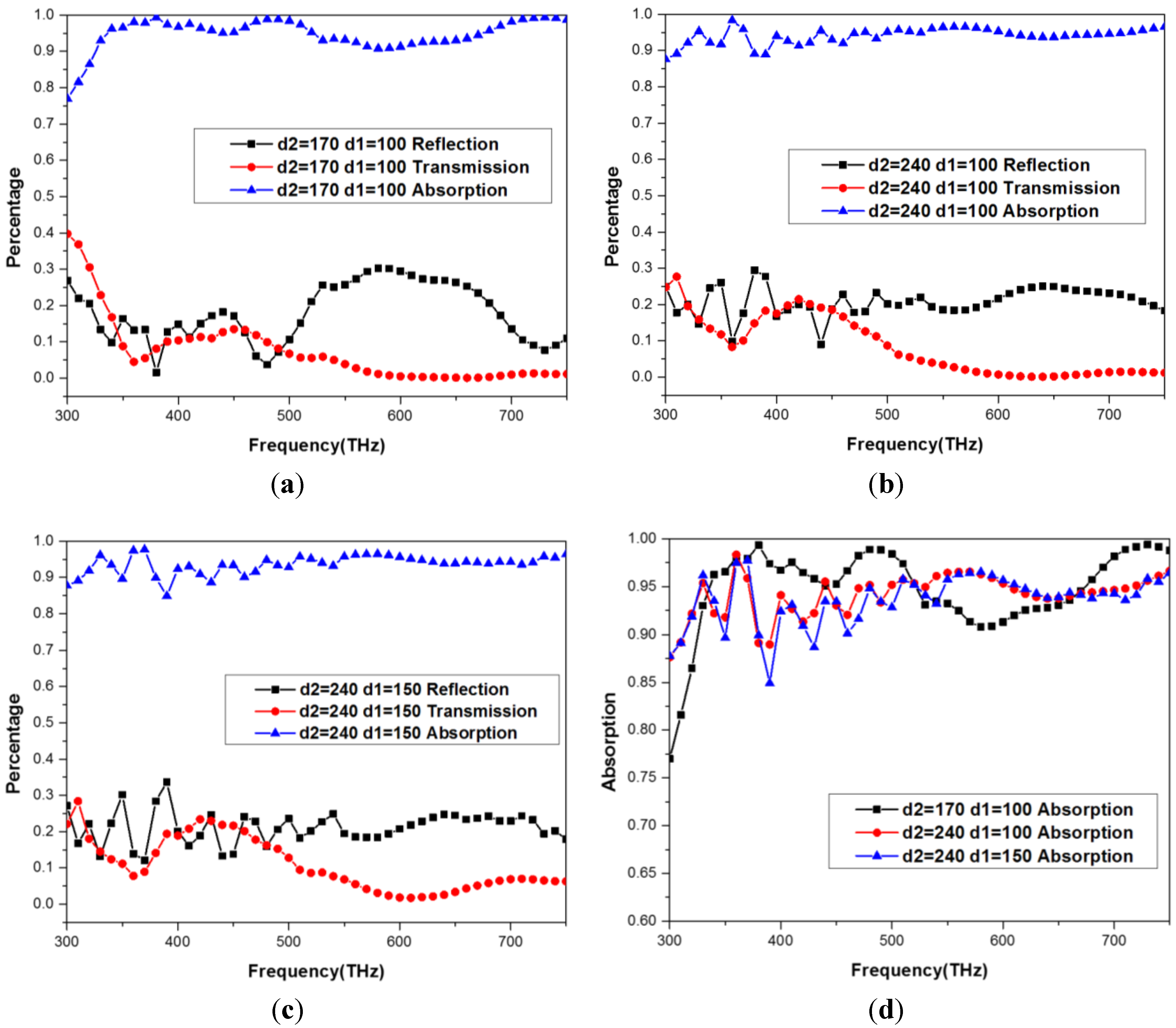
In order to optimize the proposed unit cell, a genetic algorithm (GA) is used because its interactive process can avoid local minima and, therefore, is an ideal optimization method for this particular problem. An optimal photonic structure is created using MATLAB, in combination with HFSSs Visual Basic scripting, where optimization is carried out via a GA on the proposed design. The GA mimics naïve evolution where the objective function, or in this case maximum energy absorption, is used as a measure of fitness for the system. The GA is a three-step optimization process that implements selection, crossover, and mutation over generations (iterations) in order to seek out an optimal structure topology. Through the iterative process geometric parameters, including the unit cell width,
w, thin film thicknesses
h1,
h2,
h3, and the height,
h, as well as the diameters,
d1,
d2, and the unit cell width,
w, of the core/shell are randomly selected until a global minimum is found (optimal fitness). In this case, the GA is utilized to find the geometric parameters that result in the maximum energy absorption over the entire frequency spectrum. This is accomplished by minimizing the reciprocal of the maximum energy absorption. After structural optimization is carried out, excellent absorptions with an average rate of approximately 90% can be observed over a broad high frequency range from 300 to 750 THz, as shown in
Figure 9. It can be found that optimization results are achieved in the optical spectrum, 400–1000 nm (300–750 THz), where most energy comes from and different optimized designs have different maximum absorption frequency ranges. For example, the optimized structure with
d2 = 170
di = 100 can reach the maximum absorption rate in two frequency ranges of 350–500 THz and 650–750 THz, while in 500–650 THz the absorption rate of this design is the least among all three optimized designs. The obtained optimized structures can be used in solar cells with specifically-emphasized operating frequency ranges.


