1. Introduction
Due to the intrinsic nonlinearity and fuse phenomenon in fiber, the transmission capacity in standard single-mode fiber (SMF) is reaching its upper limit of 100 Tbit/s [
1,
2,
3]. With the rapid development of 5G, cloud computing, big data, and artificial intelligence in recent years, communications based on SMF networks become difficult to meet the increasing demand for data traffic. To address this issue, a variety of multiplexing technologies, such as wavelength division multiplexing (WDM) [
4,
5], polarization division multiplexing (PDM) [
6], space division multiplexing (SDM) [
7,
8,
9,
10] have been explored to expand the transmission capacity. Practically, the WDM technique raises high standard requirements on optical modules. Meanwhile, the free-space optics-based SDM technology has to face the difficulty of precise alignment. In comparison, mode division multiplexing (MDM) based on planar lightwave circuit offers merits of low-loss and flexible processing [
11,
12,
13,
14,
15,
16,
17,
18]. With the introduction of few-mode fiber or multicore fiber, high-order modes can be utilized to carry information, which significantly increases the signal density and data transmission efficiency. Meanwhile, the power consumption of per/bit can be further reduced.
Mode multiplexers/demultiplexers (MUX/deMUX) are key components in MDM technology [
19,
20,
21,
22]. Among these diverse material solutions, silica waveguide has merits of wideband transparency, long-term stability, low-loss coupling to glass fiber, and compatibility with CMOS fabrication, allowing for the construction of optical cross-connection and add-drop multiplexing. Planar lightwave circuit (PLC)-based devices offer the advantages of compactness, low loss, and mass production. Different PLC structures used to implement the mode MUX/deMUX include multimode interference (MMI), asymmetric directional coupler (ADC), asymmetric Y-branch, microring, and gratings. Saitoh et al. proposed a two-mode multiplex/demultiplexer based on the ADCs structure with insertion loss of less than 1.3 dB and a mode extinction ratio of greater than 15 dB. A trench-type mode rotator is also proposed to convert the LP
11a mode and LP
11b mode [
23]. Though excellent in some aspects, each solution has its own deficiencies. Due to the compact size of the DC coupler, it has been adopted in silicon and polymer waveguide mode MUX/deMUX implementations. However, the loss and bandwidth issues that are crucial to the application of MDM in wide-band transmission networks are still challenges to silicon and polymer waveguide mode multiplexing devices.
In this paper, a silica waveguide mode multiplexer (MUX) consisting of four cascaded DC couplers is experimentally demonstrated. The beam propagation method is used in the device design and optimization. Thermal oxidation, plasma-enhanced chemical vapor deposition, and ultraviolet photolithography are adopted in the silica waveguide mode MUX fabrication. The measurement results prove that the input E00 mode can be selectively converted to E10 mode, E20 mode, and E30 mode. Within the wavelength range of 1500 to 1620 nm, the insertion loss is less than 12.2 dB, meanwhile. The proposed mode MUX has good potential in on-chip MDM applications.
2. Design and Optimization
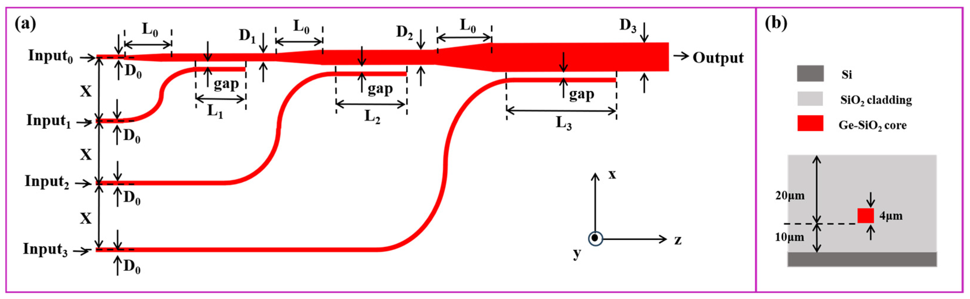
The schematic diagram of the proposed mode MUX is shown in
Figure 1a. Three DC couplers cascaded sequentially to implement the mode conversion from E
00, to E
10, E
20, and E
30. The cross-sectional view of the silica waveguide is shown in
Figure 1b. The silica waveguide is constructed on the silicon substrate. The refractive indices of silica upper-cladding and lower-cladding are both 1.4447. The refractive index of Ge-doped silica core layer is 1.4741, which forms the refractive index difference of around 2% between the core and cladding materials. The thicknesses of the upper-cladding, lower-cladding, and core layer are 20, 10, and 4 μm, respectively.
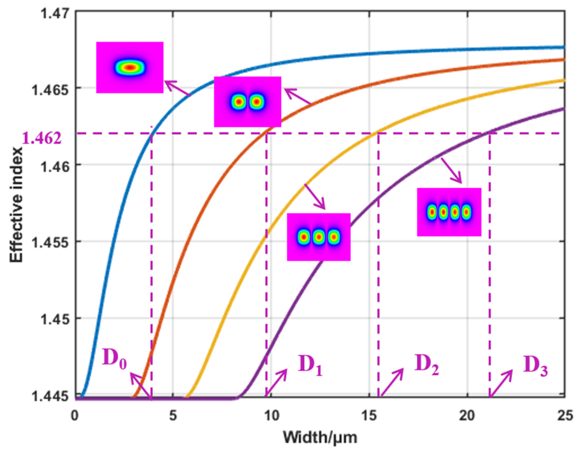
Before the waveguide size confirmation, the relationship between the effective refractive index and waveguide width at the optical wavelength of 1550 nm is calculated [
24], as shown in
Figure 2. To maintain the polarization insensitivity, the width is supposed to be the same as the height of the waveguide. Hence, the width D
0 of a single-mode waveguide is chosen to be 4 μm, which gives an effective refractive index 1.462. Meanwhile, to implement the mode conversion from the fundamental E
00 mode to the high-order E
x0 mode, the effective refractive index of E
00 mode in the single mode waveguide should be the same as that of the high-order mode E
x0 in the bus waveguide, as shown in
Figure 3. Therefore, the width of bus waveguides D
1, D
2, and D
3 are set to be 9.8, 15.7, and 21.6 μm, respectively. Under these conditions, the design of E
00 to E
x0 mode multiplexer is optimized by the beam propagation method (BPM). The coupler lengths L
1, L
2, L
3, and the gap distance between neighbored waveguides are 1300, 1660, 2000, and 2.3 μm, respectively. In order to match the spacing of the multi-channel fiber array, the spacing X between the neighbored input waveguide is 127 μm. The width of three-tapered waveguides linearly changes from D
0 = 4 μm to D
1 = 9.8 μm, D
1 = 9.8 μm to D
2 = 15.7 μm, and D
2 = 15.7 μm to D
3 = 21.6 μm, respectively. The length L
0 of the three-tapered waveguide is set to be 1000 μm to mostly restrain the loss. The overall length of the proposed mode MUX is 13,100 μm.
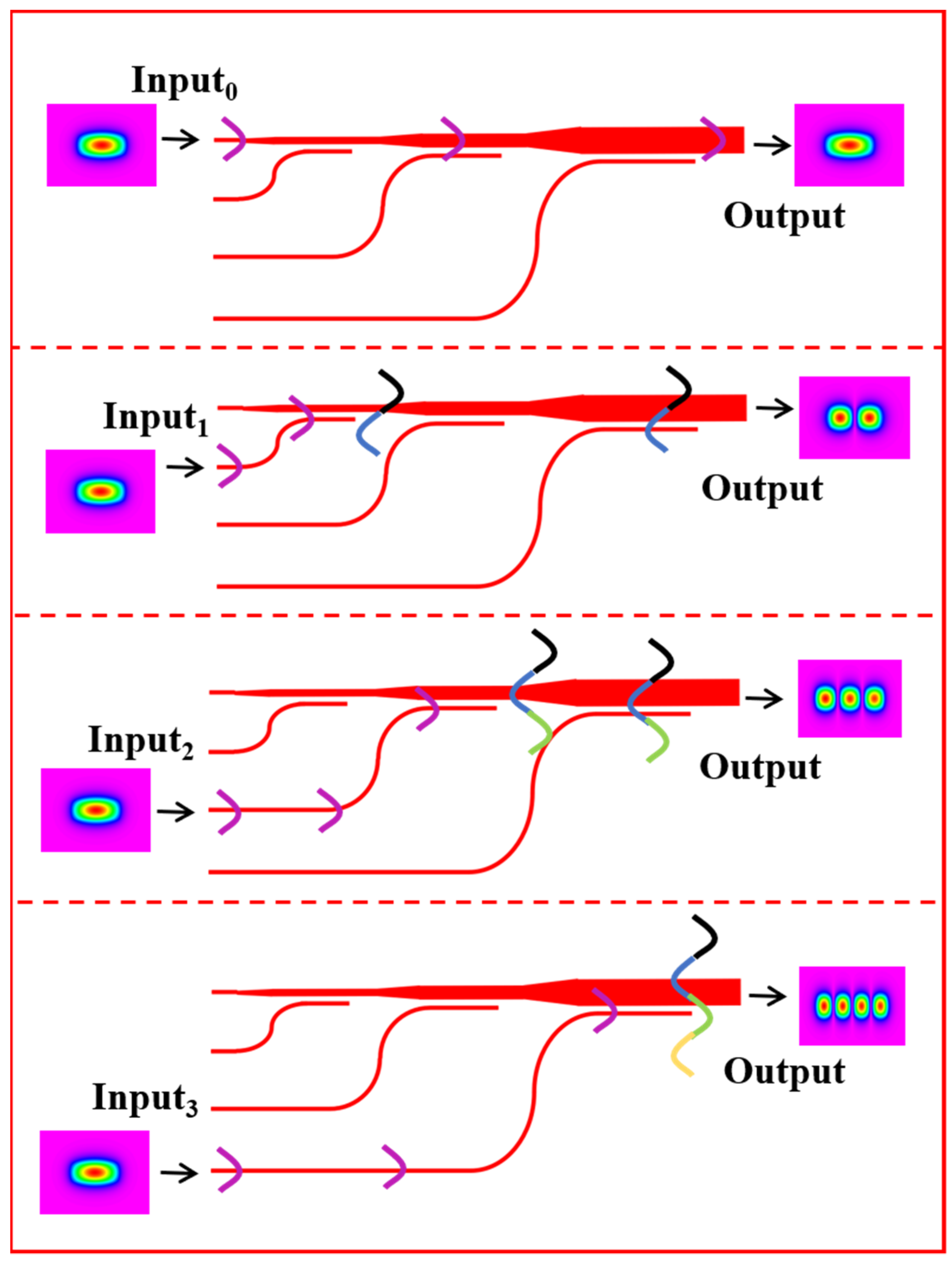
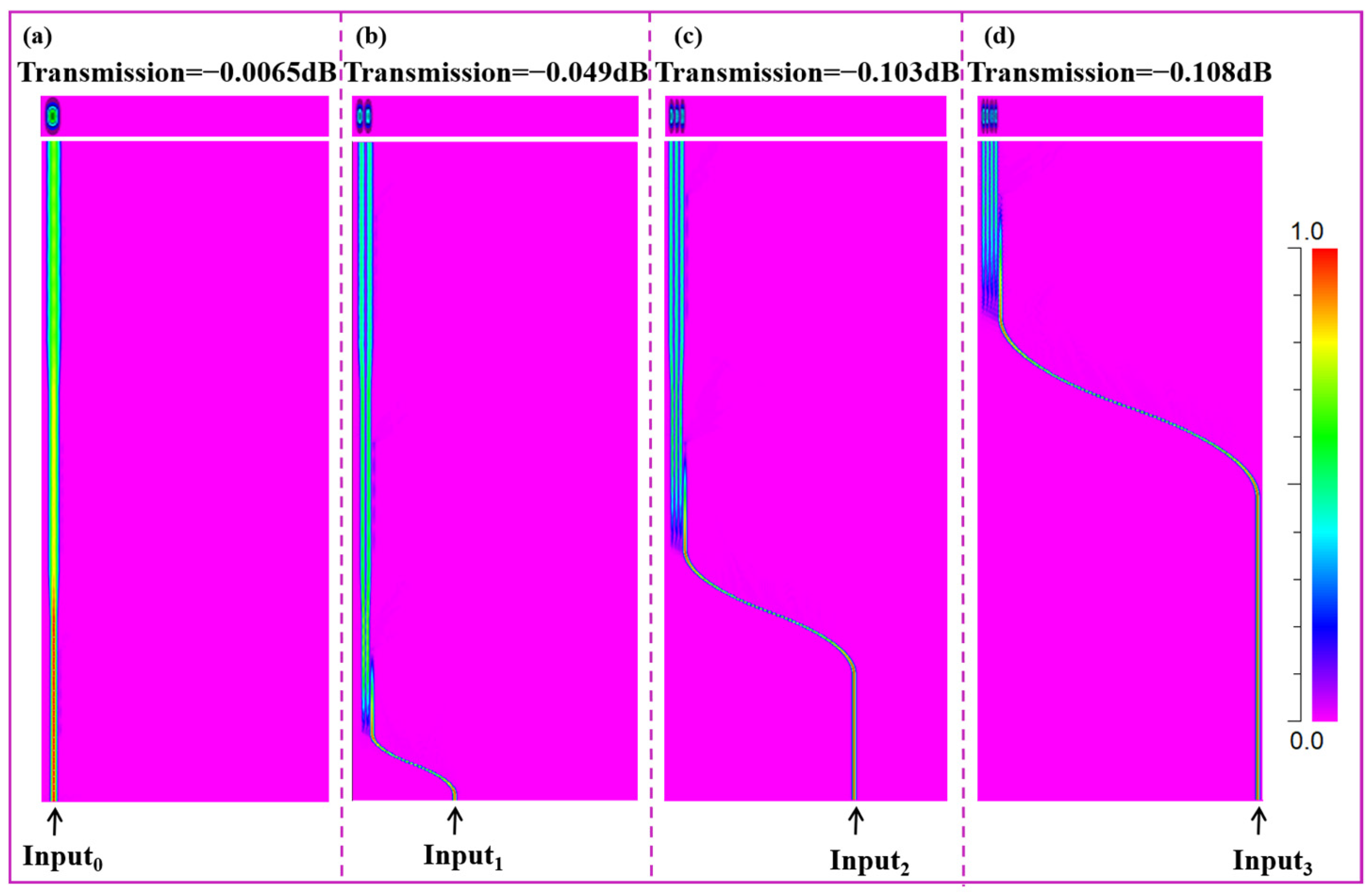
At 1550 nm, when E
00 mode is input from Input
0, Input
1, Input
2, or Input
3, the mode propagations are shown in
Figure 4. When E
00 mode is directly output from the bus waveguide, the transmittance is −0.0065 dB. When E
10, E
20, and E
30 mode is output from the bus waveguide, the transmittances are −0.049, −0.103, −0.108 dB, respectively. To be mentioned, the fiber-waveguide coupling induced loss that plays a key role in practical case is neglected here.
The bandwidth is a key characteristic for a mode MUX. The transmission of output mode as a function of optical wavelength is investigated and shown in
Figure 5. Here, −1 dB bandwidth, within the wavelength range of which the transmission of mode power drops 1 dB from the peak value, is adopted in this work. When the light input from Input
0, Input
1, Input
2, and Input
3, within the wavelength range from 1500 to 1620 nm, the transmittance of all modes is less than −0.92 dB. Since 1550 nm is chosen as the center wavelength in the investigation, the low-loss transmission mainly happens in the C-band. To be noted, the mode MUX is designed with respect to the rules of silica platform (SHIJIA Ltd., CN), which is convenient to the fabrication.
Since only the mode MUX part is experimentally implemented in this work, the theoretical investigations on the mode crosstalk are conducted. In theoretical simulations, the mode MUX is connected to a deMUX with exactly the same structure. When the single mode is input from Input
0, Input
1, Input
2, and Input
3, respectively, the single-mode outputs are recorded. Then, the calculated mode crosstalk can be obtained, as shown in
Figure 6a–d. Here, mode CT are calculated based on Equation (1):
where P
target and P
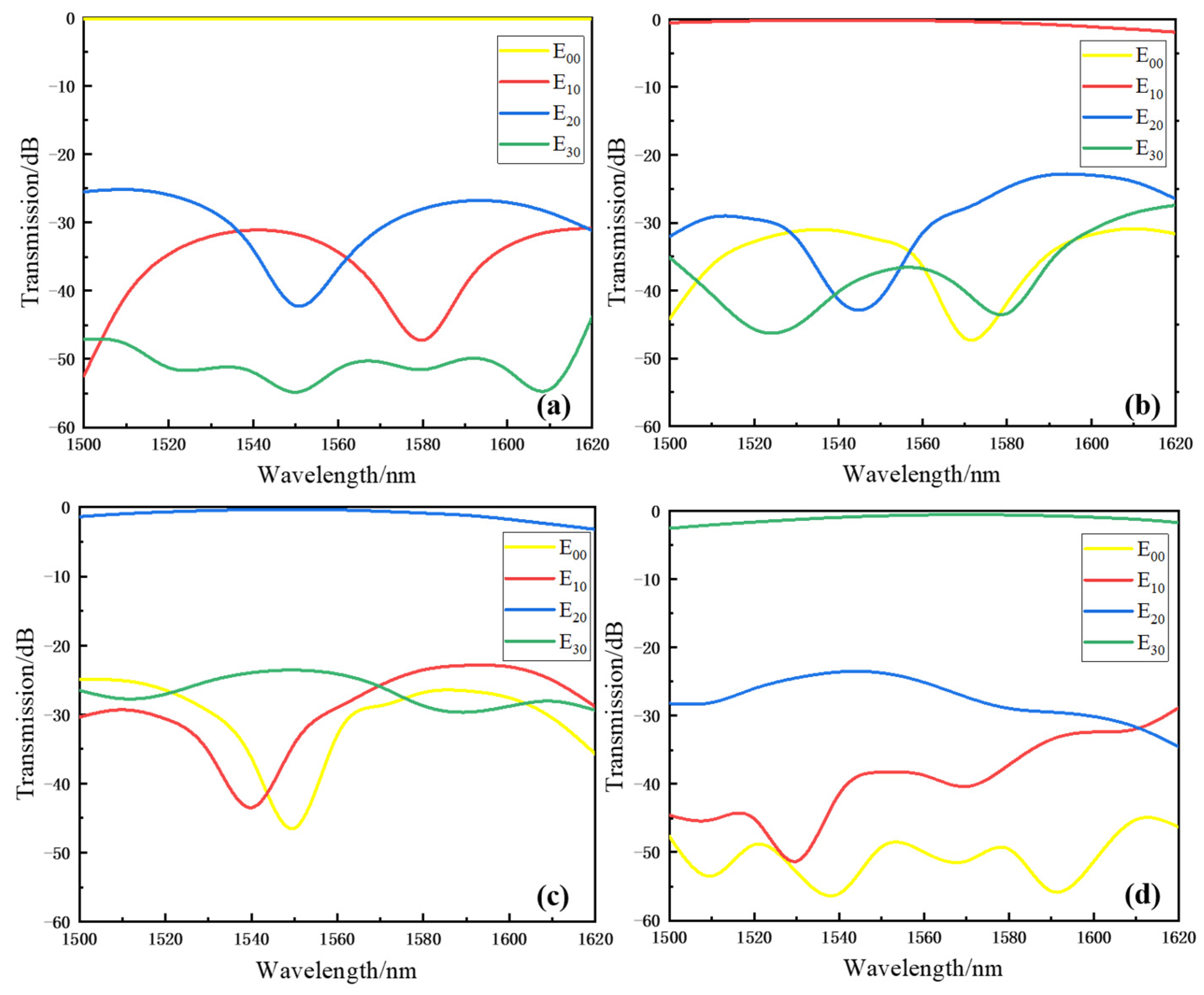
other represent the optical power output from the target mode and the power output from non-target modes. At 1550 nm, mode CTs are −31.8, −31.5, −24.2, and −23.9 dB, respectively. The bandwidth is greater than 120 nm (1500–1620 nm) under the condition that CT of all modes is less than −21.3 dB.
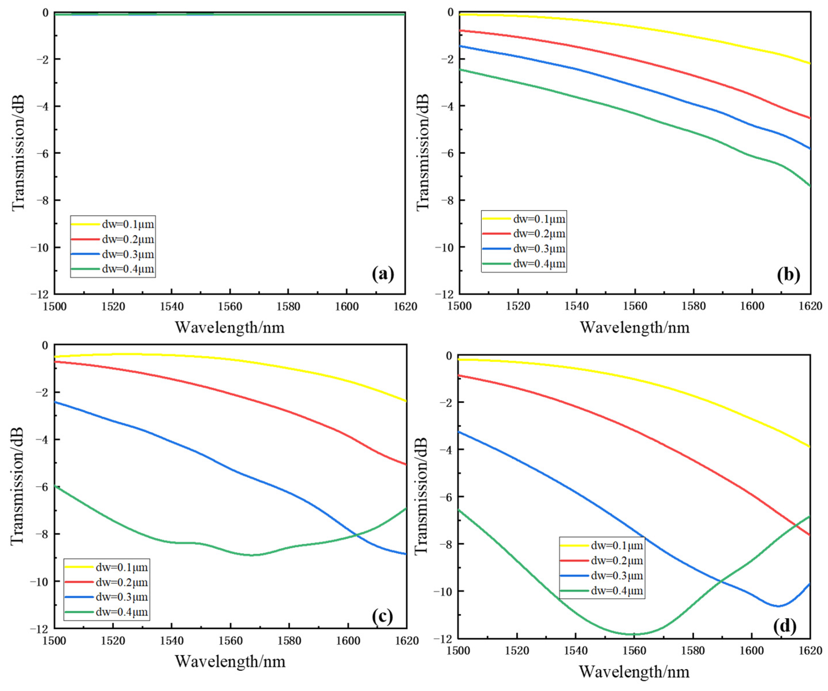
The fabrication error will cause the geometric size of waveguide deviates from the theoretical value, which would alter the effective refractive index of waveguide, and then affect the mode propagation. Simulations has been done to confirm this fabrication error induced output variation. Here, the complete width of DC coupler that includes the waveguide width and gap distance is fixed. Therefore, the increment of waveguide width dw implies the shrinkage of gap size.
Figure 7a–d are transmissions of output E
00, E
10, E
20, and E
30 mode as a function of wavelength, when dw is 0.1, 0.2, 0.3, and 0.4 μm, respectively. It can be seen that no obvious output change happens for E
00 at different dw. The transmission loss drops remarkably with the increment of wavelength for E
10, E
20 and E
30 mode, when dw increases from 0.1 to 0.4 μm. More serious scenarios happen for higher order E
20 and E
30 modes when dw is enlarging. This passive effect will lead to the notable increment of IL. Further, the blueshift phenomenon of wavelength response as a whole can be observed. These theoretical expectations of fabrication error induced output change can explain the measured experimental results.
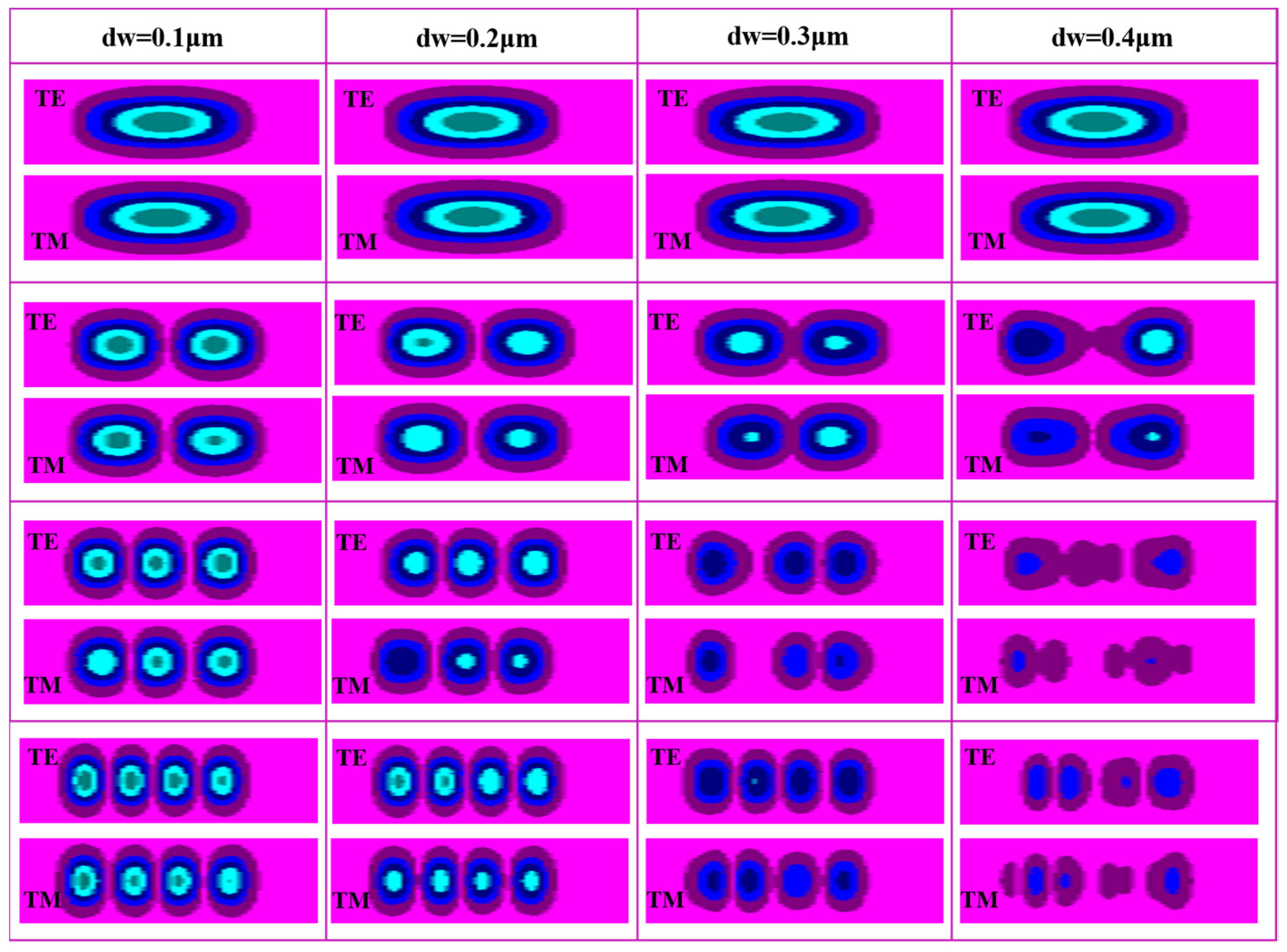
The impact of fabrication error on the polarization insensitivity is investigated, too. Here, DC coupler width change compared to the theoretical value is considered. For simplicity, the complete width of DC coupler that includes the width of waveguides and the width of gap is fixed. Therefore, the increment of waveguide width implies the shrinkage of gap size. The simulations show that no remarkable issue of polarization sensitivity exists for all modes, when the waveguide width change dw is smaller than 0.2 μm, as shown in
Figure 8. When dw in the DC coupling region is 0.3 or 0.4 μm, the polarization insensitivity deteriorates for E
10, E
20, and E
30 modes. Therefore, the waveguide size is supposed to be well controlled in the fabrication.
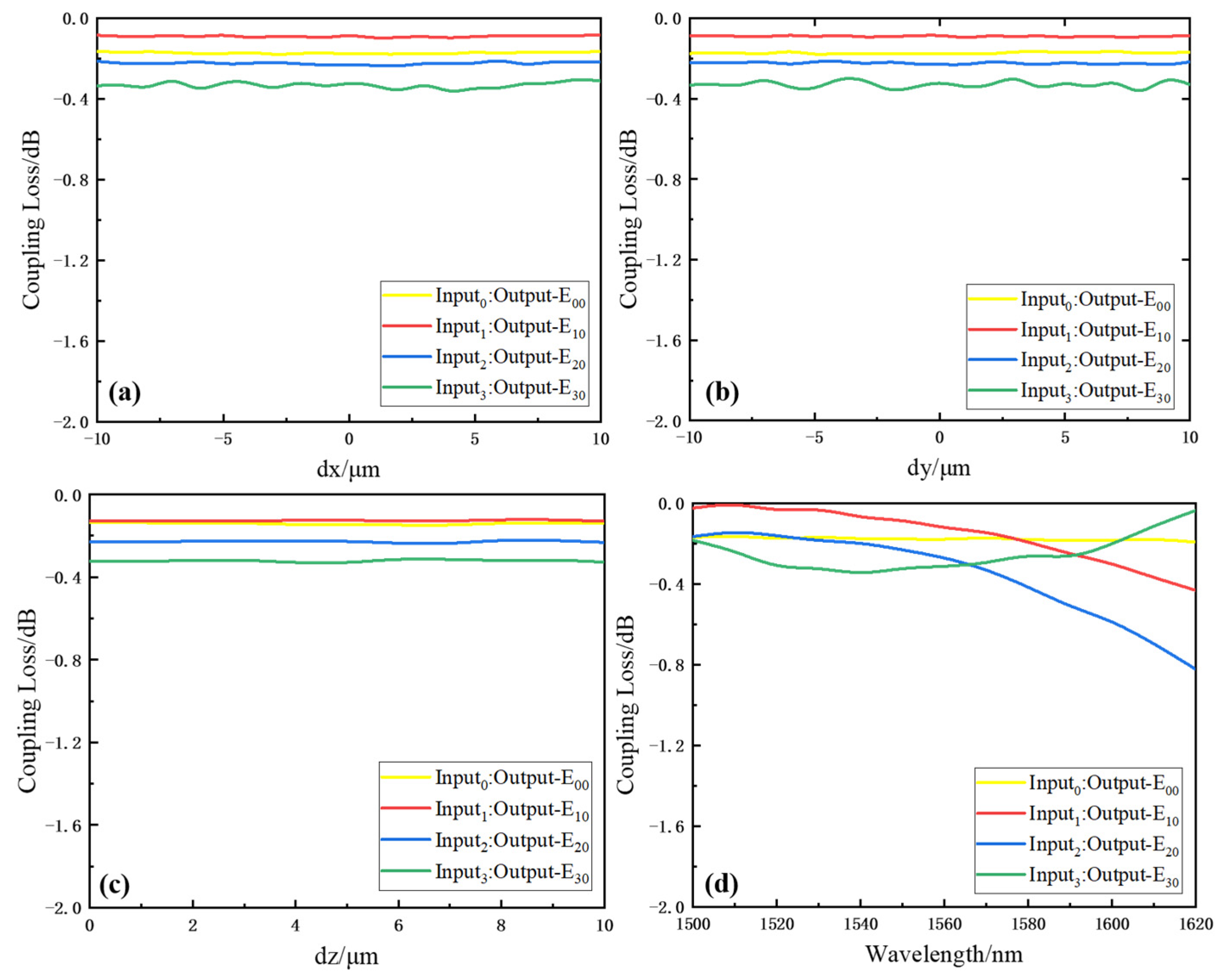
The alignment tolerance of fiber to waveguide is also a key characteristic. Since the coupling loss between SMF and the single-mode waveguide is already known. The coupling loss between the multimode fiber and bus waveguide is main factor of insertion loss. This loss originates from the intrinsic mode size difference between the rectangular bus waveguide and the large size multimode fiber, as well as the misalignment between them. Then, the coupling loss is investigated according to the constructed coupling model, which includes factors of both the geometric misalignment and the difference of mode field distribution.
Figure 9a–c below show the coupling loss at different dx, dy, and dz. Here, dx, dy, and dz represents the distance between the multimode fiber center and the output waveguide center in the x, y, and z direction, respectively. The results show that the increment of coupling loss is less than 0.4 dB for all modes, when the geometric misalignment ranges from −10 to 10 μm. The coupling loss is insensitive to the relative positions of the fiber and the waveguide. Therefore, the coupling loss mainly results from the mode field distribution difference between the multimode fiber and the rectangular shape bus waveguide. Moreover, the coupling loss as a function of wavelength is also studied. Obviously, the coupling loss of higher order modes is more sensitive to the variation of wavelength. It is worth mentioning that the coupling losses in
Figure 9 only represent the loss due to the coupling between the multimode fiber and the bus waveguide at the output end. The coupling loss at the input end and the loss of mode propagating along the silica waveguide will be included in the experimental characterization in
Section 4.
3. Fabrication and Characterization
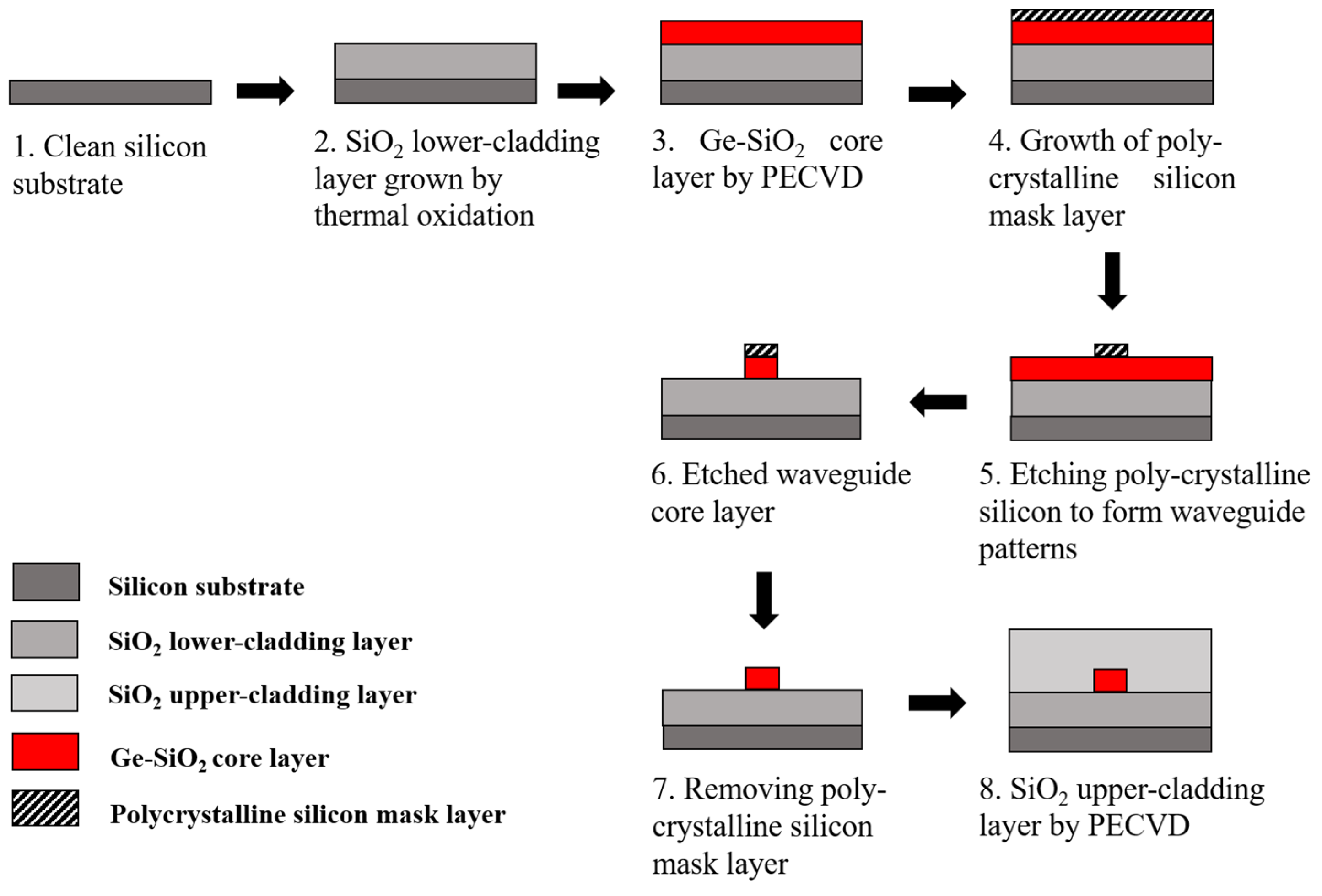
The design after optimization is fabricated according to the process flow shown in
Figure 10. Firstly, the thermal oxidation was conducted to grow the 10 μm thick silica layer on the surface of cleaned silicon substrate as the low refractive index lower-cladding. The core layer was sequentially deposited by the plasma enhanced chemical vapor deposition (PECVD) processing on the lower-cladding surface. The refractive index of silica core was adjusted by germanium (Ge) doping. By tuning the deposition rate, the thickness of high refractive index silica core layer is controlled to be 4 μm. Thereafter, poly-crystalline silicon was deposited on the high refractive index silica film as the mask layer. Then, the ultraviolet photolithography and inductively coupled plasma (ICP) etching were conducted to form the silica waveguide. Next, 20 μm-thick low refractive index silica upper-cladding was deposited by another PECVD process on the surface of silica waveguides.
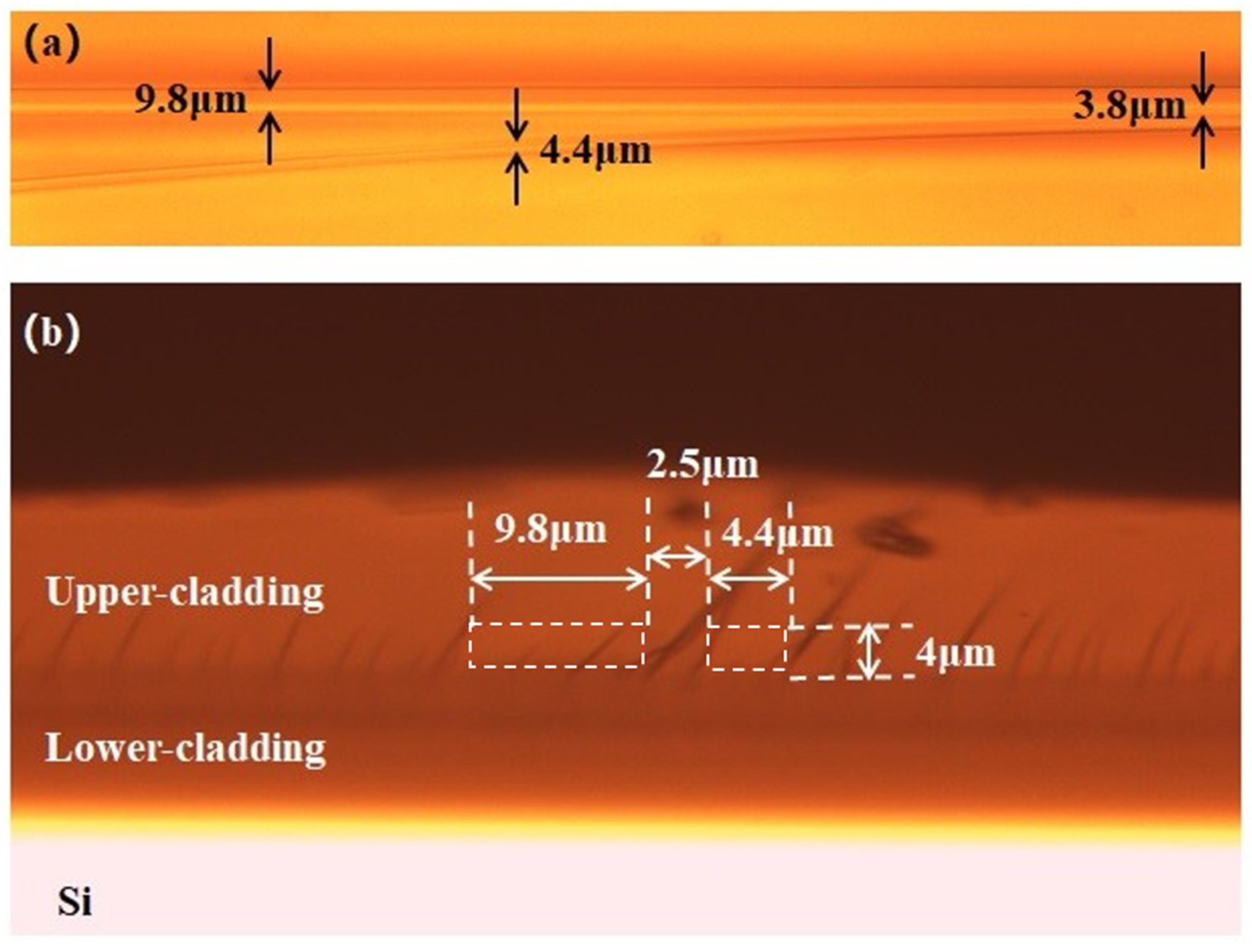
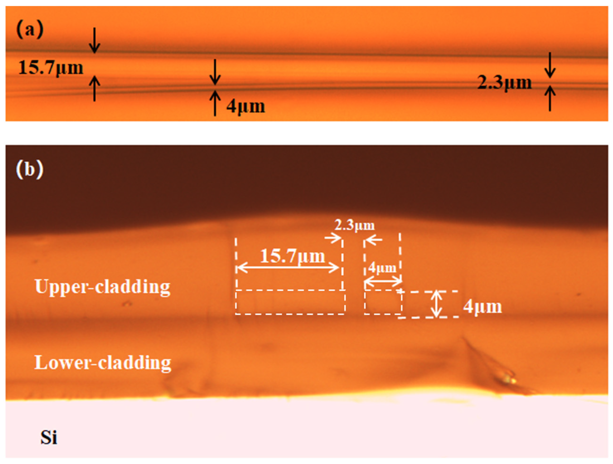
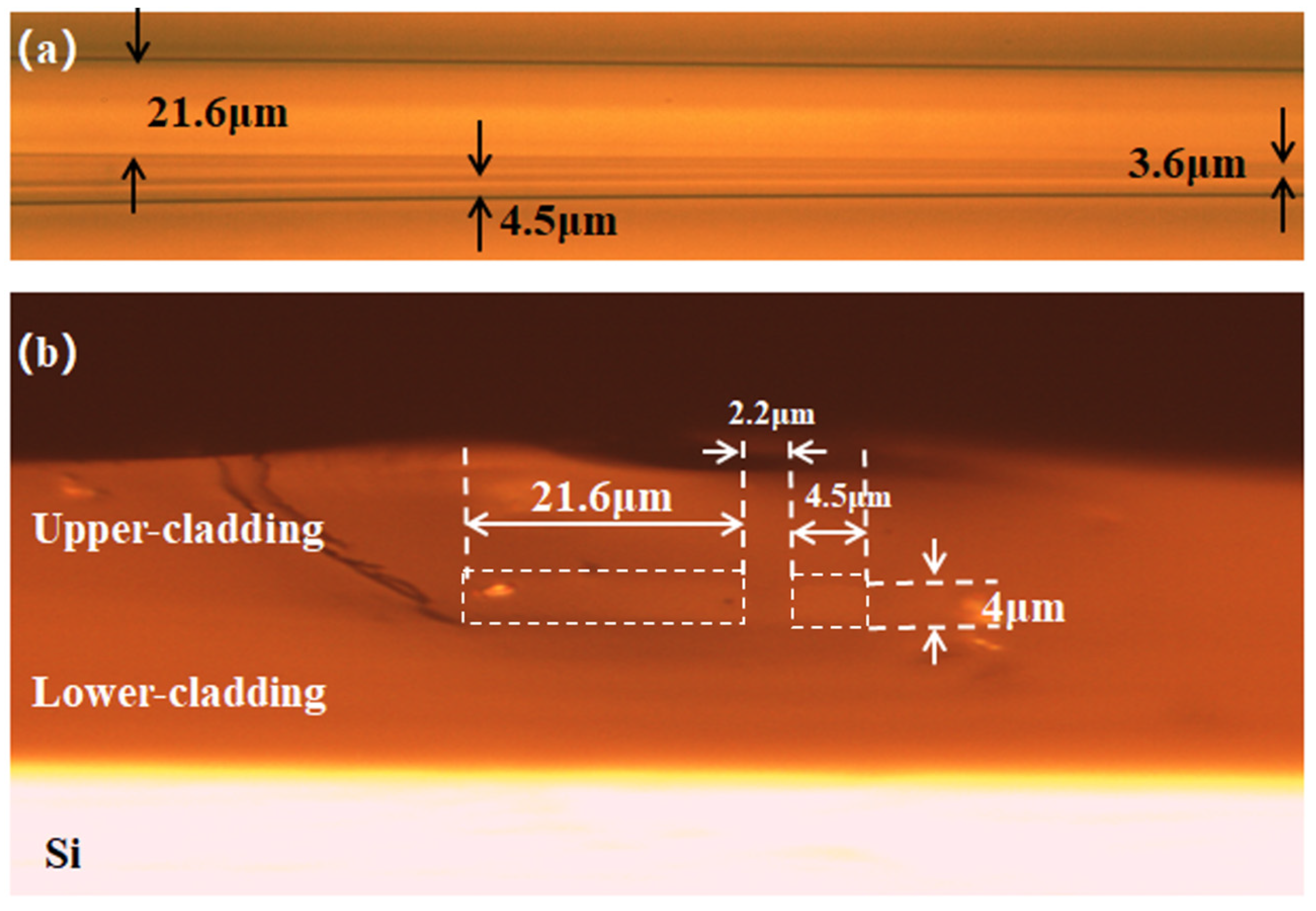
Details of fabricated DC couplers in mode MUX are characterized by optical microscope.
Figure 11,
Figure 12 and
Figure 13 are optical microscope images of DC couplers for the E
00 to E
10, E
00, to E
20, and E
00 to E
30 mode conversion, respectively. It can be seen that the dimensions of fabricated waveguides basically coincide with the theoretical design parameters. The gap distances of DC couplers are all around 2.3 μm. The difference in gap size in
Figure 11a,b results from the difference of observing position. In
Figure 11a, 3.8 μm indicates the gap distance in the transitional section, in which S-bend is used to connect the input single-mode waveguide and the straight waveguide in the DC coupling region. The gap size of 2.5 μm in
Figure 11b is obtained from the cross-sectional view in the DC coupling section. The same scenario exists in
Figure 13a,b.
Meanwhile, the waveguide is considered to be a square waveguide to achieve polarization insensitivity. However, in manufacturing, fabrication errors can cause waveguides to be trapezoidal with a narrow top and a wide bottom, resulting in some impact on polarization insensitivity. After wafer dicing and polishing, the input end of mode MUX chip was packaged with 4-channel SMF array to provide stable input. The output end of bus waveguide is unpackaged for the ease of mode pattern observation.
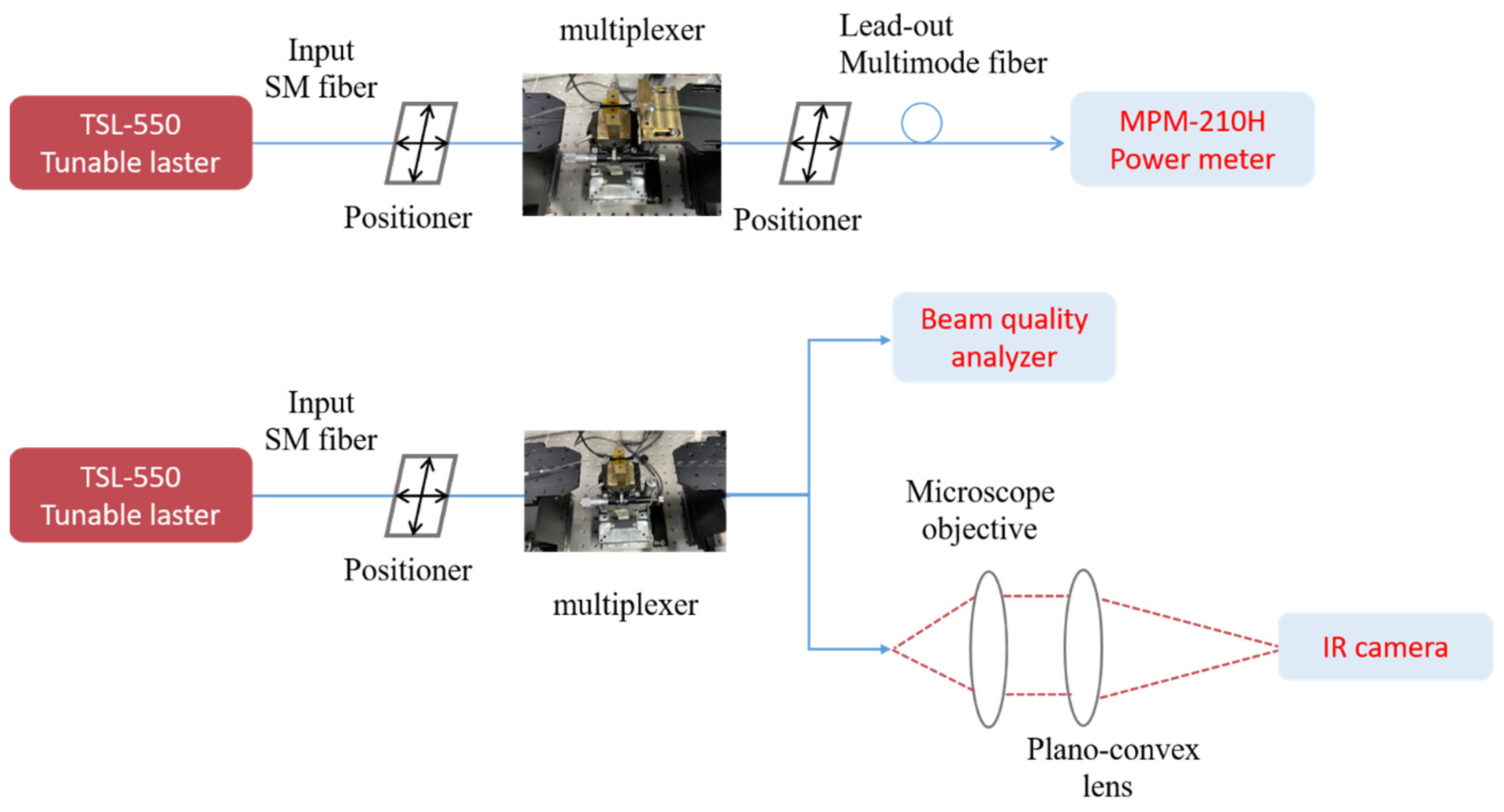
The schematic diagram of measurement setup is shown in
Figure 14. The light from a tunable laser (TSL-550, Santec Ltd., Komaki City, Japan) is coupled into the silica waveguide through a single mode fiber. The output power is recorded by an optical power meter (MPM-210H, Santec Ltd., Komaki City, Japan) through the coupling of a multimode fiber with the bus waveguide. The output mode patterns are captured by an IR camera (7290A, MiconViewer Ltd., Fairfield, CA, USA) to observed the mode pattern. The mode power distribution is recorded by the beam quality analyzer (BP209-IR, Thorlabs Ltd., Newton, NJ, USA) to estimate the performance of mode multiplexing.
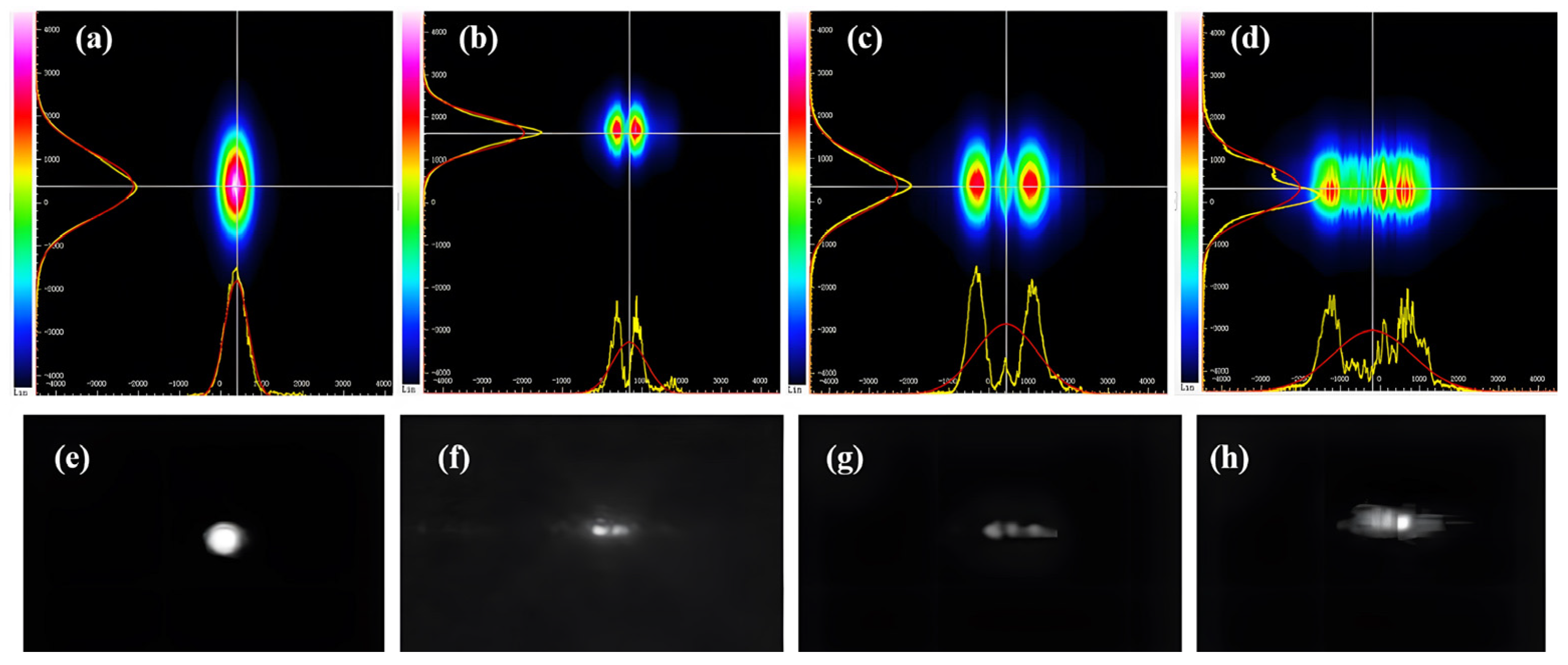
4. Results and Discussion
With the setup shown in
Figure 14, at the optical wavelength 1550 nm, the output mode patterns and profiles of MUX are recorded and shown in
Figure 15. The E
10 mode output from the bus waveguide is shown in
Figure 15a,e. The mode profile and intensity distribution exhibit the symmetric field distribution of the fundamental mode. In
Figure 15b,f, the symmetrically distributed splitting mode field coincides well with the theoretical expectation, which proves that E
00 mode has been successfully converted to E
10 mode. Similarly, E
20 mode pattern and profile can be directly observed by the IR camera and beam quality analyzer. However, the central segment of E
20 mode is relatively weak compared with sided segments, as shown in
Figure 15c,g. The captured E
30 mode pattern and profile deviate from the theoretical anticipation somehow, as shown in
Figure 15d,h. However, the mode contour profile in lateral direction is much wider than that in the case of E
10 mode and E
20 mode, which implies the mode evolution from E
00 mode to E
30 mode has happened during the mode propagation through the DC coupler. The deviation of experimental work from the ideal mode pattern in
Figure 3 mainly comes from the departure of waveguide size and gap distance from the design value. This physical deviation is inevitable in practical fabrication, as shown in
Figure 11,
Figure 12 and
Figure 13. The quality and efficiency of mode multiplexing can be improved by the elaborate design of DC coupler. Furthermore, the waveguide width change caused by the UV photolithography is supposed to be considered in the layout design to remove the fabrication error induced waveguide size change. According to the effective refractive index theory, this is beneficial to the mode evolution from the fundamental mode in the single mode waveguide to the high-order mode in the bus waveguide. The mode pattern distortion also may result from the incomplete conversion from the E
00 mode to high-order mode. The effective refractive index mismatch between E
00 mode and high-order mode will lead to the deficient mode power transfer, too.
The optical bandwidth of fabricated device is characterized, as shown in
Figure 12. Here, IL that refers to the fiber-to-fiber loss includes the transmission loss of silica waveguides and the loss induced by the input/output fiber-waveguide coupling. When the fundamental E
00 mode from the laser source is coupled into Input
0, the fiber to fiber IL of output E
00 mode is 2.19 dB at 1550 nm. Similarly, at the optical wavelength 1550 nm, when E
00 mode is coupled into Input
1, Input
2, and Input
3, respectively, ILs of E
10, E
20, and E
30 output from the bus waveguide are 4.50, 5.53, and 6.47 dB, respectively. Within the wavelength range from 1500 to 1620 nm, ILs of E
00 to E
00, E
00 to E
10, E
00 to E
20, and E
00 to E
30 mode transmission are less than 2.2, 5.5, 8.3, and 12.2 dB, respectively.
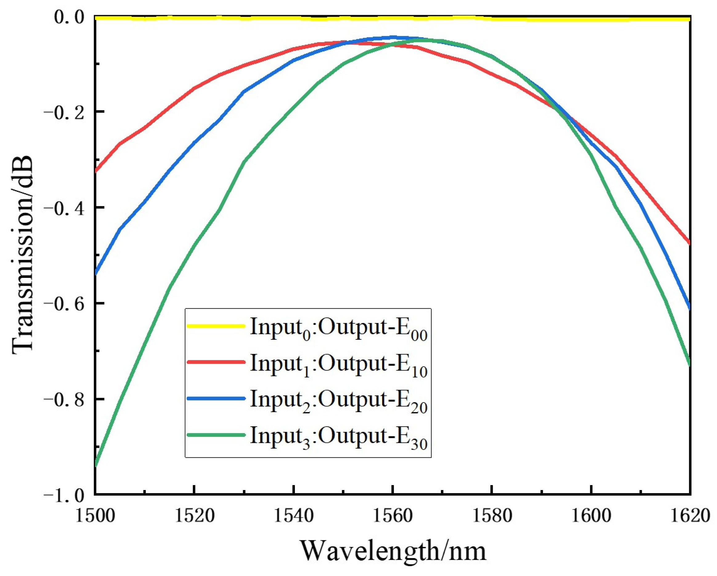
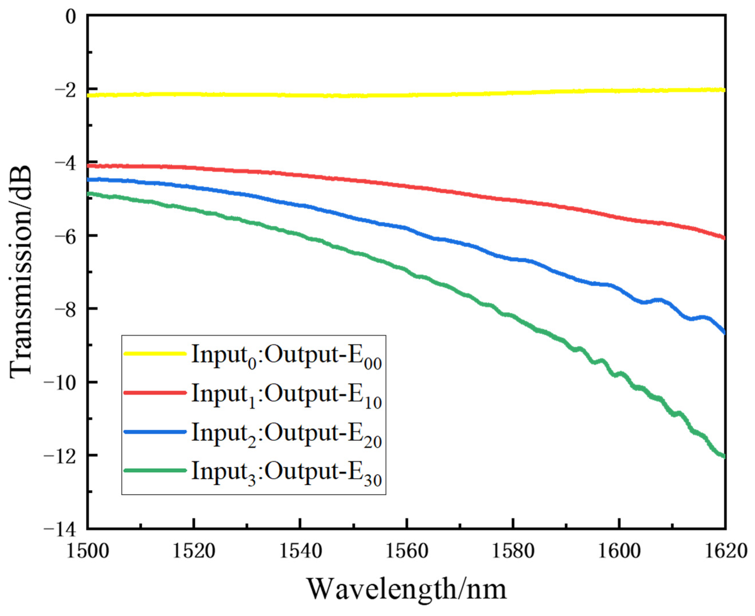
As shown in
Figure 16, the experimental 1-dB bandwidth of E
00, E
10, E
20, and E
30 are 1500–1620 nm, 1500–1570 nm, 1500–1551 nm, and 1500–1542 nm, respectively. the losses of various mode conversion almost all linearly decrease with the increment of wavelength. Compared with the theoretical bandwidth expectation, the most efficient mode evolution happens in the short wavelength region, which is different from the simulation results in
Figure 5. The wavelength response as a whole blueshifts. This shifting mainly results from the fabrication error. Since DC couplers are very sensitive to the geometric size change, the inevitable deviation of waveguide and structure size change happened in fabrication will definitely alter the wavelength response of proposed mode MUX. Another obvious difference is that the practical loss of fabricated mode MUX is much larger than that of the theoretical value, as shown in
Figure 5. It should be noted that the loss in
Figure 5 only refers to the on-chip loss, which is induced by the optical scattering and power leakage during mode propagation. Since the plasma etching caused sidewall roughness, photolithography caused waveguide shape deviation and the waveguide width and gap distance change compared to the theoretical value will lead to excess optical loss, the measured loss is certainly larger than the theoretical one. Besides, the fiber-waveguide coupling loss will increase the IL, too. For the purpose of mode pattern observation, the bus waveguide is directly coupled with the multimode fiber, which different from the commonly used SMF array coupling. To better collect the output mode power, a multimode fiber with a diameter of 62.5 μm, which is much larger than the width of bus waveguide 21.6 μm, is adopted in the experiment. The mode field mismatch between the fiber and waveguide will lead to large coupling loss. The reflections of forward propagating waveguide mode at the interface between the bus waveguide and the fiber contribute to the loss, too. Introducing a symmetric mode MUX could solve this issue. Optimized waveguide spot converters with higher coupling efficiency and improved manufacturing quality are hopeful to ameliorate the optical performance.
The performance comparison with reported works is summarized in
Table 1 below. Compared to the reported works, four mode channels are implemented in in this study. The comparable bandwidth with moderate loss performance. The increased IL mainly come from the extension to the third-order mode. Furthermore, IL here not only includes the on-chip propagation loss, but also covers the fiber-waveguide coupling. Different from the cascaded MUX/deMUX, which the input and output waveguides are both single mode waveguide, the width of exposed bus waveguide for observation is mesh smaller than the multimode waveguide. The coupling at the output end is much larger than the loss caused by the SMF and single mode waveguide. Since the coupling loss caused by the SMF and single mode waveguide is only about 0.4 dB according to our measurement, supposing the cascaded MUX/deMUX structure is adopted, the overall IL will be reduced remarkably. In summary, the MDM performance of this work is a compromised choice between conflict interests.

 ,
, 


