Communication

High-Responsivity Planar Photodetector Based on Methylammonium Lead Bromide Perovskite Thin Film

Institut Lumière-Matière, CNRS UMR5306, Université Lyon 1, Université de Lyon, 69622 Villeurbanne, France
*
Author to whom correspondence should be addressed.
Photonics 2023, 10(9), 1043; https://doi.org/10.3390/photonics10091043
Submission received: 19 July 2023 / Revised: 7 September 2023 / Accepted: 12 September 2023 / Published: 14 September 2023
(This article belongs to the Special Issue Perovskite Materials and Optoelectronic Applications)

Abstract

:
We have fabricated planar interdigitated photodetectors exhibiting high responsivity. These detectors are based on thin layers of methylammonium lead bromide (MAPbBr3) at 90 nm thickness. MAPbBr3 thin films were first characterized on glass (borosilicate) substrates using absorption and photoluminescence measurements showing a high absorption edge at 521 nm and strong emission at 530 nm, as expected. MAPbBr3 thin films were then deposited on top of interdigitated electrodes, hence producing planar photodetectors with responsivity up to 0.4 A/W. Such higher performances were attributed to the interdigitated design, low crack density (0.05 µm−2), and lower resistivity (20 MΩ.cm) compared to MAPbBr3 single crystal. Therefore, this work highlights MAPbBr3 thin films as very promising for photodetection applications.

1. Introduction

Organic–inorganic hybrid perovskites (OIHPs) thin films based on methylammonium lead halide materials are widely studied for optoelectronics, including solar cells [1,2,3], light-emitting diodes [4], solar concentrators [5], scintillators [6], and photodetectors [7,8], since they present economical, fast, and easy fabrication processes as solutions [1,4,7,8]. For photodetectors, two designs are mainly studied: the vertical design [9,10,11] with an electric field (E-field) perpendicular to the layer and the horizontal design [12] with an E-field within the plane of the layer. For the horizontal configuration, the application of the E-field parallel to the substrate prevents short circuits that can potentially happen along the unavoidable thin-film cracks. Furthermore, it presents the advantage of simpler designs and processing by depositing the OIHP layers on top of patterned electrodes. For these reasons, many horizontal photodetectors have been studied for methylammonium lead iodide (MAPbI3) [13,14], methylammonium lead chloride (MAPbCl3) [15], or methylammonium lead bromide (MAPbBr3) [16,17,18,19,20,21,22,23]. For MAPbBr3, horizontal photodetectors have many advantages like room temperature crystallization and high stability and detection in the visible range [20,21,22,23,24,25]. They have been studied with transistor designs [22], micro-wires [26], single crystals [18,27], and thin films with face-to-face [20,28] or interdigitated electrodes [23]. In these cases, thin-layer MAPbBr3 has very good properties for photodetection since they present perovskite structure with defects or doping, providing efficient carrier collection for photoconductive applications. For usual layers (without transistor designs [22]), responsivities are still limited to the maximal value of 55 mA/W [23] due to inhomogeneous layers [23] and the designs that do not use combs [20,28,29]. Such limitations can be attributed to the use of very small electrodes or non-homogeneous layers. Therefore, the development of high-quality MAPbBr3 layers on top of larger electrodes such as the interdigitated comb design is highly needed to increase the responsivity of such promising detectors.
In this work, we report the fabrication of planar photodetectors based on 90 nm thick MAPbBr3 layers. The layers were first characterized using absorption and photoluminescence measurements. Photodetectors based on interdigitated electrode combs were then fabricated, with layers presenting low crack density. The spectral dependencies were measured for different wavelengths. Finally, in order to better understand the measured responsivity, electrical properties were investigated for different distances between the electrodes.

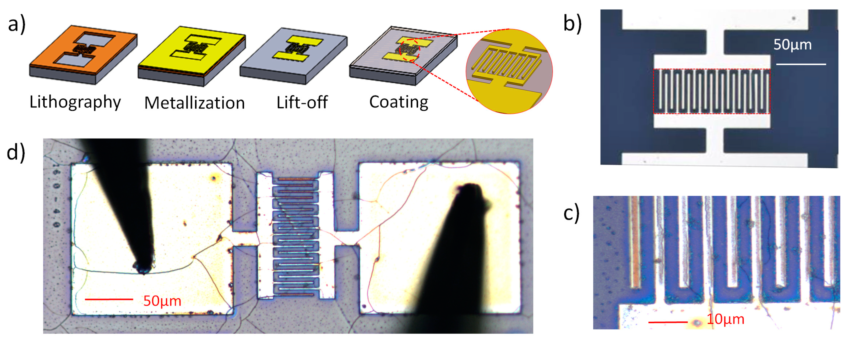
2. Materials and Methods

Figure 1a presents the process flow for the fabrication of planar photodetectors. Interdigitated combs [30] are first patterned using laser lithography (µPG101, Heidelberg Instruments, Yokohama, Japan) with a GDS file on a BK7 substrate. A negative photoresist (AZ5214(En), MicroChemicals) was spin-coated at 3000 rpm and insolated at 50 mJ/cm2 with 60 s development time. Cr/Au (10/300 nm) layers were then coated on top of the sample by sputtering deposition followed by lift-off processing using acetone. The period between the interdigitated electrodes is 8 µm, and the distance is 4 µm. Finally, the MAPbBr3 thin film was deposited on top of the patterned substrate. MAPbBr3 thin films were prepared following the anti-solvent method described in [31]. Briefly, 112 mg of methylammonium bromide (MABr, 99.8%, Sigma Aldrich, St. Louis, MO, USA) powder and 367 mg of lead bromide (99.999%, perovskite grade, Sigma Aldrich) were dissolved in 2 mL of anhydrous Dimethylformamide (DMF 98%, Sigma Aldrich), leading to a 0.5 M solution of MAPbBr3 precursor. In total, 100 μL of that solution was drop-casted on a microscope coverslip (BK7) at 5000 rpm for 30 s. Five seconds after starting the spin coater, 500 μL of Chlorobenzene (99%, Sigma Aldrich) was injected to enforce the homogeneous crystallization of the MAPbBr3 thin film. The result is a crystalline thin film with a thickness of 90 nm measured using atomic force microscopy (AFM).
Figure 1b–d present microscopic images of the fabricated photodetectors after the liftoff (Figure 1b), after coating (Figure 1c), and during electrical measurements (Figure 1d). As observed in Figure 1c,d, the layers are homogeneous since crack density has been typically evaluated at only 1 crack every 50 µm in the region of interest. Such linear crack density between the inter-digitated electrode gives a surface crack density of 0.05 µm−2. This value demonstrates good layer uniformity compared to other works [23].

3. Results

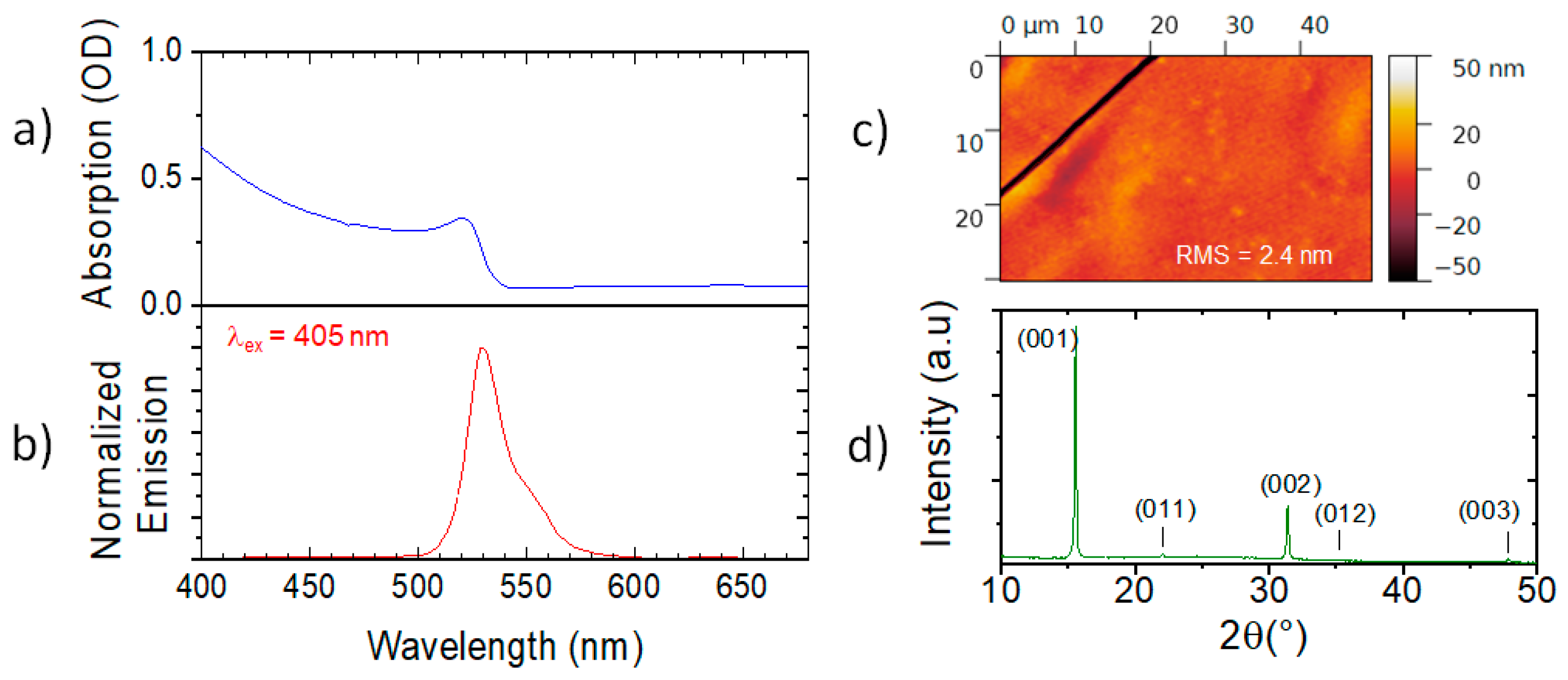
3.1. Perovskite Thin Layers
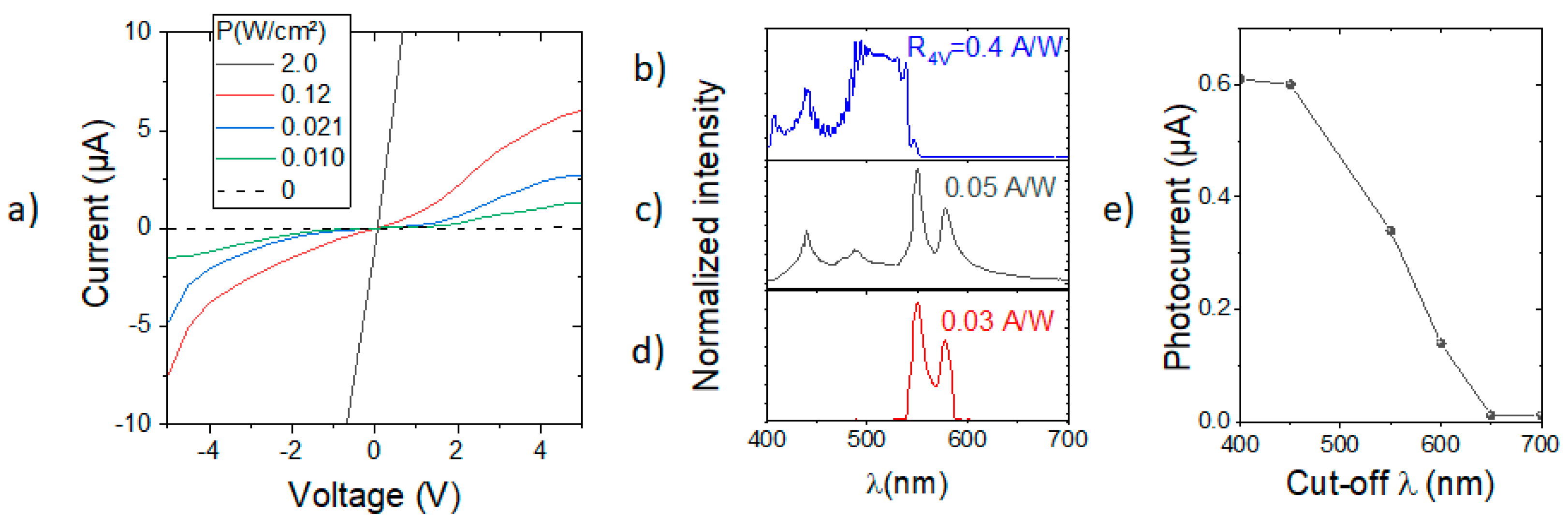
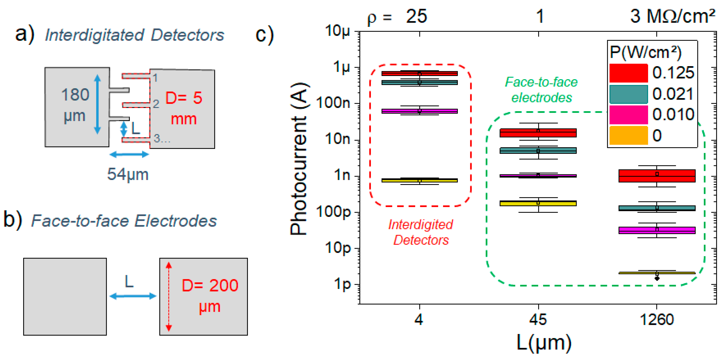
Figure 2 presents the optical properties of the studied layers deposited on the BK7 substrate without electrodes and measured using a spectrofluorometer (Edinburgh Instr., FS-5, Livingston, UK). Measurements were performed at room temperature. The photoluminescence measurement (Figure 2b) shows strong emission peaking at 530 nm with 20 nm full width half maximum. The shoulder peaks at around 550 nm can potentially be attributed to active sub-bandgap defects, which are detected at wavelengths as long as 600 nm [32,33,34]. For the absorption spectrum (Figure 2a), the absorption exhibits an exciton peak at 521 nm, as expected from similar MAPbBr3 thin films [35]. No significant signals were detected for longer wavelengths for both absorption and photoluminescence measurements.
Figure 2c shows the topography of a film measured using Nanosurf Atomic Force Microscopy (AFM). AFM measurements were performed using Nanosurf-EasyScan2 equipment with a TAP190ALG-10 probe in tapping mode. A crack was observed on the left top corner, which enabled the determination of a film thickness of ~90 nm. The roughness value was measured relative to the cracks using Gwyddion software, giving a root mean square (RMS) value at 2.4 nm. Figure 2d presents the measured X-ray diffraction (XRD) of such films. A 2θ scan was performed using an AERIS PAN-analytic instrument from 5 to 45° and Cu-Kα radiation at λ = 15,406 Å with a step size of 0.0109° and counting time of 40 s. XRD measurements confirm the fabrication of a monocrystalline film [36].

3.2. Photodetectors

Current versus voltage (I-V) curves were measured under illumination using a microscope (Eclipse LV100, Nikon), an electrical probe station, and a source/multimeter (2401, Keithley). In our study, ×10 magnification and a 16 mm working distance were used to achieve enough distance between the objective and the contacted sample. Light power P was measured without the sample with a usual power meter. Figure 3a presents the I-V curves of the sample illuminated with the blue light spectrum presented in Figure 3b. The lamp spectra were measured using a fiber-coupled spectrometer (USB4000, Ocean optics), with the fiber replacing the microscope camera. The I-V curves under illumination were plotted with the colored full lines, and the I-V curve without light was plotted with black dashed lines. Firstly, we directly observe that almost no current is detected without light (~1 nA at 1 V), which confirms that the electrodes are not short-circuited. Under illumination, the current increases with light, and responsivity increases with voltage, as expected [16,17,18,20,21,22,23].
The responsivities R at 4 V and 0.125 W/cm2 light excitation intensity have been extracted for three different wavelength ranges of excitations. The different spectra of the lamp used for this experiment are presented in Figure 3b–d with the corresponding responsivities. Responsivity R was calculated using the following formula:
R = I P · S   ,
where I is the detected photocurrent, S is the detector surface (9720 µm2 indicated by the red dashed line in Figure 1b), and P is the light power density (indicated in the inset of Figure 3a). The responsivities of 0.4, 0.05, and 0.03 A/W are measured for the spectra presented in Figure 3b–d, respectively. The influence of the excitation light was also investigated using long-pass filters placed in front of the detection path, with different cut-off wavelengths ranging from 400 to 700 nm. We present in Figure 3e the detected photocurrent as a function of the cut-off wavelength of the long-pass filters at 1 V using the lamp spectra presented in Figure 3c at 0.125 W/cm2 light excitation intensity. The non-zero photocurrent detected for a cut-on wavelength at 600 nm is a signature of active sub-bandgap defects and intrinsic disorder in the Urbach tail of MAPbBr3, defects which are detected at wavelengths as long as 600 nm [31,32,33,34,37].
In order to better understand the responsivities measured in Figure 3, we have compared the photogenerated currents for different devices. The interdigitated combs with 4 µm distance previously studied (Figure 4a) were compared to face-to-face electrode pads with a 200 × 200 µm2 surface and distances of L = 45 and 1260 µm (Figure 4b). Figure 4c presents the averaged current (for a statistic over 10 measurements) as a function of the excitation light intensity for the three different designs, including interdigitate electrodes at 1 V polarization. Results are presented on a log scale to capture their full dynamics. Furthermore, layer resistivity ρ was also extracted from such data using the following equation:
ρ = D · e L · r   ,
L is the distance between the electrodes, r is the measured resistance of the MAPbBr3 thin film in between the electrodes, D is the effective width of the electrode (the values of D are indicated in Figure 4a,b, corresponding to the dashed red lines) and the thickness of the MAPbBr3 thin film. We found a resistivity of ρ = 25, 1, and 3 MΩ·cm for L = 4, 45, and 1260 µm, respectively.

4. Discussion

As presented in Figure 3b, the highest responsivity is reported for blue light excitation since the absorption of the perovskite layer is high in this spectral region (Figure 1b). Furthermore, a higher photocurrent is also detected in Figure 3e for cut-on wavelengths below 500 nm (close to the MAPbBr3 bandgap). The spectral behavior of the photoconductive devices is thus closely related to the layer’s properties, as expected. For suitable input light, a maximum responsivity of 0.4 A/W is demonstrated. Such a value is seven times higher than the highest values reported in the literature so far for similar devices due to our interdigitate design [20,21] and the better layer uniformity compared to [23].
To further understand such high responsivity, we can compare the different devices presented in Figure 4. We clearly see that the generated photocurrent is higher with the interdigitated electrodes (L = 4 µm in Figure 4c) compared to the face-to-face electrodes (L = 45 and 1260 µm in Figure 4c) given the following responsivities: 0.1, 0.001, and 10−6 A/W for L = 4, 45 and 1260 µm, respectively. Note that the interdigitated responsivity is lower than the one in Figure 3 because a voltage of only 1 V was used here, giving a minimum noise equivalent power of 10 nW. Therefore, the generated photocurrent appears to be highly related to the dark current. The charge collection is thus more efficient for the interdigitated electrodes compared to the face-to-face electrodes. Such tests confirm the interest in the interdigitate design. For resistivity (indicated at the top part of Figure 4c), comb resistivity (L = 4 µm) is higher compared to face-to-face designs with larger L distances, probably due to the Schottky barriers that have a higher influence on shorter distances [38]. Since no resistivity has been reported so far for MAPbBr3 thin films in the literature, we can only compare these values with single-crystal MAPbBr3 values. In this case, resistivity is lower than single crystals that are typically closer to GΩ.cm [39]. This behavior could be attributed to the higher trap density acting as residual doping [9,40]. Therefore, this relatively larger dark current (usually associated with a limitation for photodiode detectors) coming from low resistivity is an advantage here for responsivity, especially for the interdigitated design. This work thus provides perspectives on intentional MAPbBr3 doping [41,42] for detector applications.

5. Conclusions

As a conclusion, we have reported the fabrication of photodetectors based on interdigitated metallic combs with thin-film MAPbBr3 of 90 nm thickness as active layers. With respect to the photodetector with comb designs, it exhibits high responsivity up to 0.4 A/W, which is seven times larger than similar devices from the state of the art in the literature, with a spectral dependence in good agreement with their optical properties. The highest responsivity value was attributed to the comb design, low crack density (0.05 µm−2), and relatively low resistivity (25 MΩ·cm) probably due to the high trap density, allowing good charge collection for photodetection. This work thus gives a better understanding of interdigitated devices with respect to MAPbBr3 thin films used as active layers and highlights these thin layers as very promising candidates for the fast fabrication of economical devices for optoelectronic applications.

Author Contributions

Conceptualization, A.G. and J.H.; methodology, A.G., B.M. and P.M.; investigation, P.M. and N.D.; resources, B.M.; supervision A.G., B.M. and J.H; writing—original draft preparation, A.G.; writing—review and editing, A.G. and J.H.; All authors have read and agreed to the published version of the manuscript.

Funding

This research has been funded by the Institute of Light Matter (UMR5306 CNRS UCBL).

Institutional Review Board Statement

Not applicable.

Informed Consent Statement

Not applicable.

Data Availability Statement

The data underlying the results presented in this paper are not publicly available at this time but may be obtained from the authors upon reasonable request.

Acknowledgments

The authors would like to thank the Nanolyon Platform for the clean room facilities. B.M. thanks the Université de Lyon PALSE program under the framework “Investissements d’avenir” (ANR-11-IDEX-0007).

Conflicts of Interest

The authors declare no conflict of interest.

References

  1. Yang, W.S.; Park, B.W.; Jung, E.H.; Jeon, N.J.; Kim, Y.C.; Lee, D.U.; Seok, S.I. Iodide management in formamidinium-lead-halide–based perovskite layers for efficient solar cells. Science 2017, 356, 1376–1379. [Google Scholar] [CrossRef] [PubMed]
  2. Mehdi, H.; Mhamdi, A.; Hannachi, R.; Bouazizi, A. MAPbBr3 perovskite solar cells: Via a two-step deposition process. RSC Adv. 2019, 9, 12906–12912. [Google Scholar] [CrossRef]
  3. Tang, M.C.; Dang, H.X.; Lee, S.; Barrit, D.; Munir, R.; Wang, K.; Li, R.; Smilgies, D.M.; De Wolf, S.; Kim, D.Y.; et al. Wide and Tunable Bandgap MAPbBr3−xClx Hybrid Perovskites with Enhanced Phase Stability: In Situ Investigation and Photovoltaic Devices. Sol. RRL 2021, 5, 2000718. [Google Scholar] [CrossRef]
  4. Ling, Y.; Yuan, Z.; Tian, Y.; Wang, X.; Wang, J.C.; Xin, Y.; Hanson, K.; Ma, B.; Gao, H. Bright Light-Emitting Diodes Based on Organometal Halide Perovskite Nanoplatelets. Adv. Mater. 2016, 28, 305–311. [Google Scholar] [CrossRef]
  5. Zhou, Y.; Zhao, H.; Ma, D.; Rosei, F. Harnessing the properties of colloidal quantum dots in luminescent solar concentrators. Chem. Soc. Rev. 2018, 47, 5866–5890. [Google Scholar] [CrossRef] [PubMed]
  6. Mykhaylyk, V.B.; Kraus, H.; Saliba, M. Bright and Fast Scintillation of Organolead Per-ovskite 479 MAPbBr3 at Low Temperatures. Mater. Horiz. 2019, 6, 1740–1747. [Google Scholar] [CrossRef]
  7. Shrestha, S.; Fischer, R.; Matt, G.J.; Feldner, P.; Michel, T.; Osvet, A.; Levchuk, I.; Merle, B.; Golkar, S.; Chen, H.; et al. High-performance direct conversion X-ray detectors based on sintered hybrid lead triiodide perovskite wafers. Nat. Photonics 2017, 11, 436–440. [Google Scholar] [CrossRef]
  8. Wu, X.; Zhou, B.; Zhou, J.; Chen, Y.; Chu, Y.; Huang, J. Distinguishable Detection of Ultraviolet, Visible, and Infrared Spectrum with High-Responsivity Perovskite-Based Flexible Photosensors. Small 2018, 14, 1800527. [Google Scholar] [CrossRef]
  9. Yang, Z.; Deng, Y.; Zhang, X.; Wang, S.; Chen, H.; Yang, S.; Khurgin, J.; Fang, N.X.; Zhang, X.; Ma, R. High-performance single-crystalline perovskite thin-film photodetector. Adv. Mater. 2018, 30, 1704333. [Google Scholar] [CrossRef]
  10. Chaudhary, J.; Choudhary, S.; Negi, C.M.S.; Gupta, S.K.; Verma, A.S. Surface morphological, optical and electrical characterization of methylammonium lead bromide perovskite (CH3NH3PbBr3) thin film. Phys. Scr. 2019, 94, 105821. [Google Scholar] [CrossRef]
  11. Xu, Z.; Zeng, Y.; Meng, F.; Gao, S.; Fan, S.; Liu, Y.; Zhang, Y.; Wageh, S.; Al-Ghamdi, A.A.; Xiao, J.; et al. A High-Performance Self-Powered Photodetector Based on MAPbBr3 Single Crystal Thin Film/MoS2 Vertical Van Der Waals Heterostructure. Adv. Mater. Interfaces 2022, 9, 1–7. [Google Scholar] [CrossRef]
  12. Wang, X.; Li, M.; Zhang, B.; Wang, H.; Zhao, Y.; Wang, B. Recent progress in organometal halide perovskite photodetectors. Org. Electron. 2018, 52, 172–183. [Google Scholar] [CrossRef]
  13. Hu, W.; Cong, H.; Huang, W.; Huang, Y.; Chen, L.; Pan, A.; Xue, C. Germanium/perovskite heterostructure for high-performance and broadband photodetector from visible to infrared telecommunication band. Light Sci. Appl. 2019, 8, 106. [Google Scholar] [CrossRef]
  14. Rong, S.S.; Faheem, M.B.; Li, Y.B. Perovskite single crystals: Synthesis, properties, and applications. J. Electron. Sci. Technol. 2021, 19, 1–18. [Google Scholar] [CrossRef]
  15. Wang, W.; Xu, H.; Cai, J.; Zhu, J.; Ni, C.; Hong, F.; Fang, Z.; Xu, F.; Cui, S.; Xu, R.; et al. Visible blind ultraviolet photodetector based on CH3NH3PbCl3 thin film. Opt. Express 2016, 24, 8411. [Google Scholar] [CrossRef] [PubMed]
  16. Zhang, Z.; Chen, K.; Xia, W.; Zuo, Z. MAPbBr3 single crystal based metal-semiconductor-metal photodetector enhanced by localized surface plasmon. Mater. Res. Express 2020, 7, 125902. [Google Scholar] [CrossRef]
  17. Chen, L.C.; Lee, K.L.; Lee, K.Y.; Huang, Y.W.; Lin, R.M. Study of metal–semiconductor–metal CH3NH3PbBr3 perovskite photodetectors prepared by inverse temperature crystallization method. Sensors 2020, 20, 297. [Google Scholar] [CrossRef]
  18. Saidaminov, M.I.; Adinolfi, V.; Comin, R.; Abdelhady, A.L.; Peng, W.; Dursun, I.; Yuan, M.; Hoogland, S.; Sargent, E.H.; Bakr, O.M. Planar-integrated single-crystalline perovskite photodetectors. Nat. Commun. 2015, 6, 4–10. [Google Scholar] [CrossRef]
  19. Gavranovic, S.; Pospisil, J.; Zmeskal, O.; Novak, V.; Vanysek, P.; Castkova, K.; Cihlar, J.; Weiter, M. Electrode Spacing as a Determinant of the Output Performance of Planar-Type Photodetectors Based on Methylammonium Lead Bromide Perovskite Single Crystals. ACS Appl. Mater. Interfaces 2022, 14, 20159–20167. [Google Scholar] [CrossRef]
  20. Jang, D.M.; Park, K.; Kim, D.H.; Park, J.; Shojaei, F.; Kang, H.S.; Song, J.K. Reversible halide exchange reaction of organometal trihalide perovskite colloidal nanocrystals for full-range band gap tuning. Nano Lett. 2015, 15, 5191–5199. [Google Scholar] [CrossRef]
  21. Choi, G.I.; Choi, H.W. A Study to Improve the Performance of Mixed Cation–Halide Perovskite-Based UVC Photodetectors. Nanomaterials 2022, 12, 1132. [Google Scholar] [CrossRef] [PubMed]
  22. Yu, H.; Yan, L.; Qiu, R.; Xu, X.; Luo, W.; Zhou, H. Ambipolar solution-processed CH3NH3PbBr3 perovskite phototransistors with ultra-thin Al2O3 protective layer. In Proceedings of the 2018 IEEE International Conference on Electron Devices and Solid State Circuits (EDSSC), Shenzhen, China, 6–8 June 2018; pp. 2–3. [Google Scholar]
  23. Wang, F.; Mei, J.; Wang, Y.; Zhang, L.; Zhao, H.; Zhao, D. Fast photoconductive responses in organometal halide perovskite photodetectors. ACS Appl. Mater. Interfaces 2016, 8, 2840–2846. [Google Scholar] [CrossRef]
  24. Zhou, S.; Wang, Q.; Xu, Z.; Xu, S.; Yang, P.; Deng, H.; Li, B.; Dong, Y.; Han, P.; Su, Y. Antisolvent solvothermal synthesis of MAPbBr3 nanocrystals for efficient solar photodecomposition of methyl orange. J. Colloid Interface Sci. 2021, 595, 98–106. [Google Scholar] [CrossRef] [PubMed]
  25. Zhu, Y.; Liu, Y.; Ai, Q.; Gao, G.; Yuan, L.; Fang, Q.; Lou, J. In situ synthesis of lead-free halide perovskite–COF nanocomposites as photocatalysts for photoinduced polymerization in both organic and aqueous phases. ACS Mater. Lett. 2022, 4, 464–471. [Google Scholar] [CrossRef]
  26. Li, X.S.; Xu, Y.S.; Li, C.L.; Guo, Q.; Wang, G.; Xia, H.; Fang, H.H.; Shen, L.; Sun, H.B. Perovskite Single-Crystal Microwire-Array Photodetectors with Performance Stability beyond 1 Year. Adv. Mater. 2020, 32, 1–10. [Google Scholar] [CrossRef] [PubMed]
  27. Zhang, Y.; Liu, Y.; Li, Y.; Yang, Z.; Liu, S. Perovskite CH3NH3Pb(BrxI1−x)3 single crystals with controlled composition for fine-tuned bandgap towards optimized optoelectronic applications. J. Mater. Chem. C 2016, 4, 9172–9178. [Google Scholar] [CrossRef]
  28. Rahil, M.; Ansari, R.M.; Ahmad, S.; Islam, S.S. Nanostructured Ruddlesden–Popper-Layered Lead Bromide Perovskites with Stable and Selected Wavelength for Photodetection Applications. ACS Appl. Nano Mater. 2023, 6, 5187–5199. [Google Scholar] [CrossRef]
  29. Shin, S.G.; Bark, C.W.; Choi, H.W. Study on performance improvements in perovskite-based ultraviolet sensors prepared using toluene antisolvent and CH3NH3Cl. Nanomaterials 2021, 11, 4. [Google Scholar] [CrossRef]
  30. Gassenq, A.; Gencarelli, F.; Van Campenhout, J.; Shimura, Y.; Loo, R.; Narcy, G.; Roelkens, G. GeSn/Ge heterostructure short-wave infrared photodetectors on silicon. Opt. Express 2012, 20, 27297–27303. [Google Scholar] [CrossRef]
  31. Baronnier, J.; Houel, J.; Dujardin, C.; Kulzer, F.; Mahler, B. Doping MAPbBr3 hybrid perovskites with CdSe/CdZnS quantum dots: From emissive thin films to hybrid single-photon sources. Nanoscale 2022, 14, 5769–5781. [Google Scholar] [CrossRef]
  32. Fu, J.; Jamaludin, N.F.; Wu, B.; Li, M.; Solanki, A.; Ng, Y.F.; Mhaisalkar, S.; Huan, C.H.A.; Sum, T.C. Localized Traps Limited Recombination in Lead Bromide Perovskites. Adv. Energy Mater. 2019, 9, 1803119. [Google Scholar] [CrossRef]
  33. Baronnier, J.; Dujardin, C.; Mahler, B.; Houel, J. Low-Temperature Emission Dynamics of Methylammonium Lead Bromide Hybrid Perovskite Thin Films at the Sub-Micrometer Scale. Nanomaterials 2023, 13, 2376. [Google Scholar] [CrossRef] [PubMed]
  34. Che, X.; Traore, B.; Katan, C.; Fang, H.H.; Loi, M.A.; Even, J.; Kepenekian, M. Charge Trap Formation and Passivation in Methylammonium Lead Tribromide. J. Phys. Chem. C 2019, 123, 13812–13817. [Google Scholar] [CrossRef]
  35. Saidaminov, M.I.; Abdelhady, A.L.; Murali, B.; Alarousu, E.; Burlakov, V.M.; Peng, W.; Bakr, O.M. High-quality bulk hybrid perovskite single crystals within minutes by inverse temperature crystallization. Nat. Commun. 2015, 6, 7586. [Google Scholar] [CrossRef] [PubMed]
  36. Wang, K.H.; Li, L.C.; Shellaiah, M.; Sun, K.W. Structural and Photophysical Properties of Methylammonium Lead Tribromide (MAPbBr3) Single Crystals. Sci. Rep. 2017, 7, 13643. [Google Scholar] [CrossRef] [PubMed]
  37. Droseros, N.; Tsokkou, D.; Banerji, N. Photophysics of Methylammonium Lead Tribromide Perovskite: Free Carriers, Excitons, and Sub-Bandgap States. Adv. Energy Mater. 2020, 10, 1903258. [Google Scholar] [CrossRef]
  38. Henisch, H.K. Metal-semiconductor Schottky barrier junctions and their applications. Proc. IEEE 1986, 74, 894. [Google Scholar] [CrossRef]
  39. Liu, X.; Fu, J.; Zhao, D.; Hao, Y.; Zhu, H.; Xu, M.; Xu, Y. MAPbBr3−xIx Crystals Improved by Accurate Solution-Grown Procedure for Alpha Particle Detection. Front. Phys. 2020, 7, 1–6. [Google Scholar] [CrossRef]
  40. Wenger, B.; Nayak, P.K.; Wen, X.; Kesava, S.V.; Noel, N.K.; Snaith, H.J. Consolidation of the optoelectronic properties of CH3NH3PbBr3 perovskite single crystals. Nat. Commun. 2017, 8, 1. [Google Scholar] [CrossRef]
  41. Ulatowski, A.M.; Wright, A.D.; Wenger, B.; Buizza, L.R.; Motti, S.G.; Eggimann, H.J.; Herz, L.M. Charge-Carrier Trapping Dynamics in Bismuth-Doped Thin Films of MAPbBr3 Perovskite. J. Phys. Chem. Lett. 2020, 11, 3681–3688. [Google Scholar] [CrossRef]
  42. Chatterjee, K.; Nayak, M.; Jahid Akhtar, A.; Saha, S.K. Sn doping enhanced current rectification in MAPbBr3 nanocrystal-metal junction for photodetection. Mater. Today Proc. 2022, 66, 3205–3210. [Google Scholar] [CrossRef]
Figure 1. (a) Process flow for detector fabrication starting with lithography and metallization, followed by liftoff and film coating. Top image of fabricated photodetectors (b) after liftoff, (c) after the perovskite deposition, and (d) during the opto-electrical characterization.
Photonics 10 01043 g001
Figure 2. Optical properties of a MAPbBr3 thin film on a BK7 substrate with its(a) absorption spectrum and (b) normalized photoluminescence excited at λ e x c = 405 nm. (c) AFM measurement for the MAPBBr3 layer on SiO2 showing low roughness relative to a detected crack and (d) XRD pattern of the film.
Photonics 10 01043 g002
Figure 3. Opto-electrical characterization with the (a) I−V curve as a function of the light intensity for short wavelength light (blue light). Spectra and corresponding responsivities measured at 4 V for (b) short wavelength input light (blue light), (c) white light, and (d) long wavelength light (green light). (e) Wavelength dependence of the photocurrent as a function of the cut-on wavelength when a filter is placed on the beam path of the white lamp.
Photonics 10 01043 g003
Figure 4. Schematic pictures for (a) the interdigitate and (b) face-to-face designs; (c) photocurrent as a function of the light intensity for both interdigitated and face-to-face designs at 1 V.
Photonics 10 01043 g004
Disclaimer/Publisher’s Note: The statements, opinions and data contained in all publications are solely those of the individual author(s) and contributor(s) and not of MDPI and/or the editor(s). MDPI and/or the editor(s) disclaim responsibility for any injury to people or property resulting from any ideas, methods, instructions or products referred to in the content.

