Article

Density-Functional Study of the Si/SiO2 Interfaces in Short-Period Superlattices: Vibrational States and Raman Spectra

by
Mikhail Smirnov
1,*,
Evgenii Roginskii
2,
Aleksandr Savin
1,2,
Aleksandr Oreshonkov
3,4,* and
Dmitrii Pankin
5
1
Faculty of Physics, Saint-Petersburg State University, Universitetskaya nab. 7/9, Saint-Petersburg 199034, Russia
2
Laboratory of Spectroscopy of Solid State, Ioffe Institute, Politehnicheskaya St. 26, Saint-Petersburg 194021, Russia
3
Laboratory of Molecular Spectroscopy, Kirensky Institute of Physics, Federal Research Center KSC SB RAS, Akademgorodok St. 50/38, Krasnoyarsk 660036, Russia
4
School of Engineering and Construction, Siberian Federal University, Svobodny pr. 82, Krasnoyarsk 660041, Russia
5
Center for Optical and Laser Materials Research, Research Park, Saint-Petersburg State University, Universitetskaya nab. 7/9, Saint-Petersburg 199034, Russia
*
Authors to whom correspondence should be addressed.
Photonics 2023, 10(8), 902; https://doi.org/10.3390/photonics10080902
Submission received: 22 June 2023 / Revised: 22 July 2023 / Accepted: 24 July 2023 / Published: 4 August 2023

Abstract

:
Raman spectroscopy has proven its effectiveness as a highly informative and sensitive method for the nondestructive analysis of layered nanostructures and their interfaces. However, there is a lack of information concerning the characteristic phonon modes and their activity in Si/SiO2 nanostructures. In order to overcome this problem, the phonon states and Raman spectra of several Si/SiO2 superlattices (SL) with layer thicknesses varied within 0.5–2 nm are studied using DFT-based computer modeling. Two types of structures with different interfaces between crystalline silicon and SiO2 cristobalite were studied. A relationship between the phonon states of heterosystems and the phonon modes of the initial crystals was established. Estimates of the parameters of deformation potentials are obtained, with the help of which the shifts of phonon frequencies caused by elastic strains in the materials of the SL layers are interpreted. The dependence of intense Raman lines on the SL structure has been studied. Several ways have been proposed to use this information, both for identifying the type of interface and for estimating the structural parameters. The obtained information will be useful for the spectroscopic characterization of the silicon/oxide interfaces.

1. Introduction

The structure and electronic properties of the oxide-semiconductor interfaces were widely investigated because the efficiency of many electronic devices depends on them. Silicon dioxide (SiO2) is predominantly used for the fabrication of the oxide layers in silicon-based electronics. Special interest is given to the fabrication of light-emitting and photoresponse multilayer and superlattice Si/SiO2 structures, including Si nanocrystals (see, e.g., [1,2,3,4,5]). It needs the investigation of interface quality as well as defect formation, especially oxygen vacancies [6], which can strongly affect the optical properties, e.g., luminescence properties [1]. A lot of studies were devoted to elucidating the structure and properties of the Si/SiO2 interfaces [7,8,9,10,11,12,13]. Many of them used computer simulation approaches based on rigorous quantum mechanical calculations [13,14,15,16,17,18,19,20,21,22,23,24,25,26,27,28,29]. The objects of such studies were either free-standing 2D periodic slabs [13,14,15,16,17,18,19] or 3D periodic superlattices [20,21,22,23,24,25,26,27,28,29]. The first approach is conceptually simpler but is inevitably associated with the problem of modeling external surfaces with dangling bonds. The second approach is free from this complication but requires more time-consuming calculations. An additional advantage of the second approach is that the considered superlattices can actually be synthesized and used in various optoelectronic devices [10,11,12].
A serious problem in the theoretical study of heterostructures is the choice of a spatial model. As a rule, the initial configuration is chosen based on the crystal structure of the initial materials. In this case, these are crystalline silicon and one of the crystalline modifications of silica. The final structure is found through geometry optimization. As applied to heterostructures, the result of such modeling depends on the choice of one or another polymorphic modification of SiO2. To choose the most adequate one, it is necessary to go through all possible variants and compare their energies of formation.
Such assessments were made in relation to several interface Si with different polymorphs of SiO2: cristobalite [14,15,18,21,22,23,24,28,29], quartz [13,15,17,23,26], and tridymite [15,18,19,23,25]. However, in any case, a structure obtained during the optimization process must be stable. To check the stability, it is necessary to count the phonon spectrum and make sure that there are no phonons with imaginary frequencies in the entire Brillouin zone (BZ). In none of the papers known to us, such a check has been carried out. This study aims to fill this gap.
We intend to test various structural models of the Si/SiO2 interface to calculate the phonon spectrum for each of them and evaluate its stability against atomic displacements. In addition, it is planned to carry out modeling of the Raman spectrum of the studied systems, which will make it possible to reveal their characteristic spectroscopic features. Raman spectroscopy, as a method based on the inelastic scattering of light by atomic vibrations, provides information on the frequencies and polarization properties of phonons, on the basis of which it is possible to draw conclusions about the details of the spatial and electronic structure of crystals. This research technique has proven its effectiveness as a highly informative and sensitive method for non-destructive analysis of not only crystals but also heterostructures such as superlattices. It has been shown in a number of works that the analysis of Raman spectra can be used to estimate the layer thicknesses, the quality of the interfaces, and the tensions in the layer materials with high accuracy (see [30] and references therein). As applied to Si/SiO2 SLs, the use of Raman spectroscopy [31,32,33,34,35,36] made it possible to obtain valuable information about the layer structure and the annealing temperature and to estimate the crystallite size and the stress magnitudes. In the study [35], it was possible to use information on the frequency position of the spectral lines to estimate the layer thicknesses. However, no one has yet analyzed the obtained Raman spectra by applying rigorous quantum mechanical calculations. This article presents the results of a theoretical study of the vibrational spectra of two possible types of Si/SiO2 SLs, which can be considered the first step towards a comprehensive study of the structure-spectrum relationship for these heterostructures, which are important for practical applications.
As applied to Si/SiO2 SLs, the use of Raman spectroscopy [31,32,33,34,35,36,37] made it possible to obtain valuable information about the layer structure and the annealing temperature and to estimate the crystallite size and the stress magnitudes. In [38], only one of the simplest representatives of the SL family was considered. In [39], the results for several SLs with different layer thicknesses were presented. Two interface structures were considered. The interface type I1 is based on the direct splicing of two cubic lattices of silicon and β-cristobalite in the [001] direction. The interface type I2 implies the rotation of one of the lattices by 45° around the SL axis. It is found that in both cases, the silicon lattice conserves its quasi-cubic structure, whereas the oxide lattice is markedly deformed by rotations of the SiO4 tetrahedra around the SL axis. Such tetrahedron rotations transform cubic β-cristobalite into the tetragonal β ˜ -cristobalite. This transformation ensures the flexibility of the cristobalite lattice and allows it to form smooth interfaces with the silicon lattice despite the large lattice mismatch. The structures of I1 and I2 SL are shown in Figure 1a and Figure 1b, respectively.
In the studied heterostructures, there are Si atoms in different oxidation states. The Si4+ state is inherent to the atoms within the oxide material (upper part of Figure 1), and the Si0 state occurs inside the silicon material (bottom part of Figure 1). One can see that the main difference concerns the thickness of the interface layer. It consists of one monolayer of the Si2+ moieties in the I1 structure and two monolayers of Si2+ and Si1+ moieties in the I2 structure. Thus, the presence of the Si1+ atoms and the Si1+–Ob–Si1+ bridges is the most obvious structural peculiarity of the I2 SL.
We considered several SLs of both types with different layer thicknesses, denoting them by the double indices m × n, where m is the number of Si monolayers in the silicon layer and n is the number of SiO2 bilayers in the oxide layer. The structures and energies of the SLs were discussed in [38,39]. This article presents the results on the phonon states and Raman spectra of these SLs.

2. Computational Details

The ab initio calculations using the plane-wave pseudopotential method were carried out within the framework of density functional theory in the generalized gradient approximation (GGA) approximation using the PBEsol functional [40] as realized in the ABINIT software package [41,42,43]. The norm-conserving pseudopotentials were constructed according to the scheme described in [44]. For Si and O atoms, the 3s3p and 2s2p electrons were treated as the valence ones, respectively. The plane-wave basis size was controlled by the cutoff energy Ecut = 45 Ha. The BZ sampling according to the Monkhorst-Pack scheme [45] was chosen as 6 × 6 × 2. The full geometry optimization was performed by varying both the lattice parameters and atomic positions. The convergence tolerance for geometry optimization was selected within 10−5 Ha/Bohr and 0.01 GPa in the maximal force and stress tensor, respectively. Each self-consistent step was controlled by energy convergence lower than 108 Ha. The phonon eigenvectors, frequencies, and Raman tensor components were calculated at the Г-point of the BZ within the density functional perturbation theory (DFPT) [46,47]. The Raman spectra were simulated using Lorentzian line shape functions with full width at a maximum of 8 cm1.

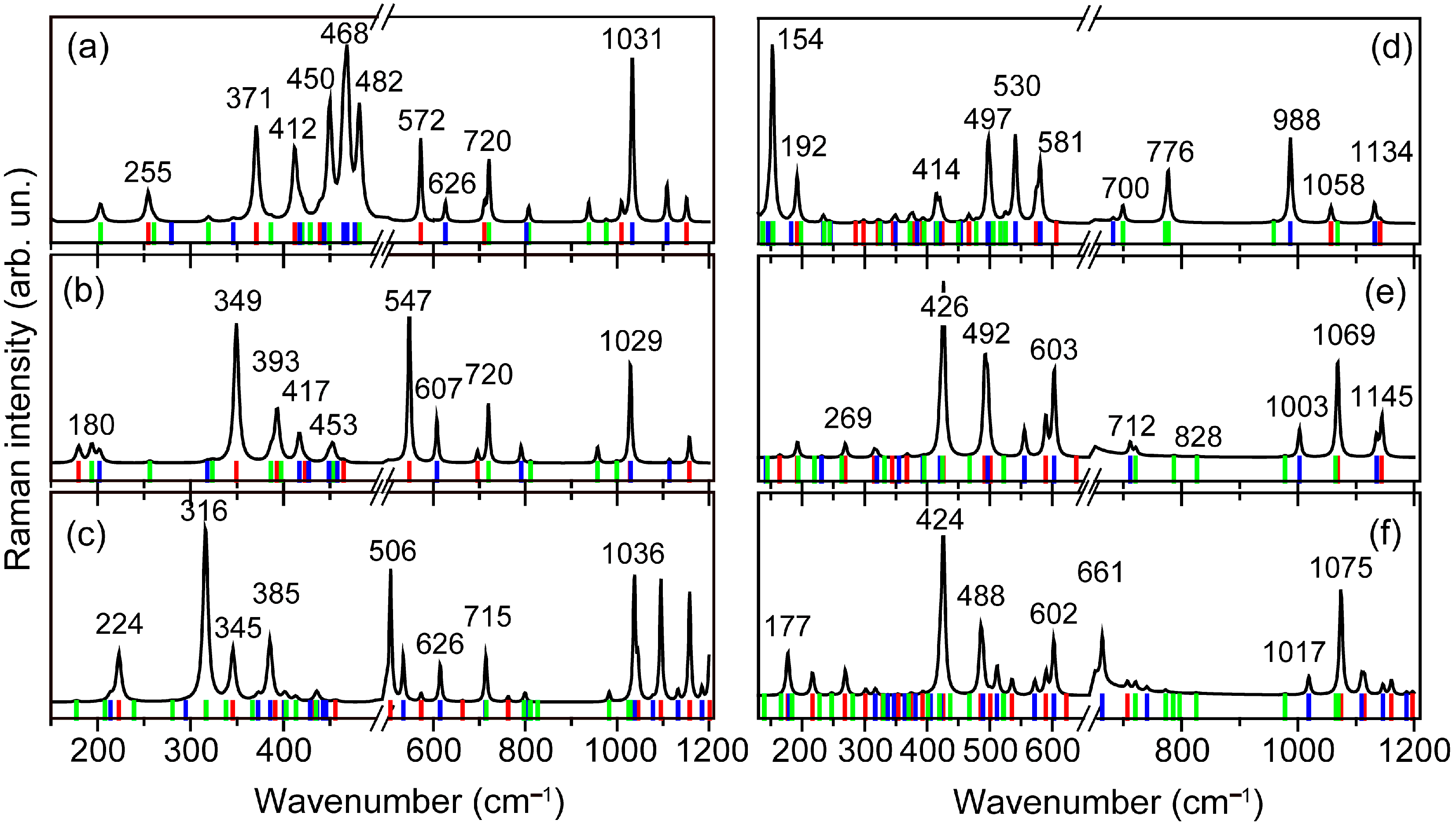
3. Results and Discussion

3.1. Bulk Crystals

Before proceeding to the analysis of the phonon spectra of SL, it is worth discussing the spectra of the constituent bulk materials. By the way, this will allow estimating the performance of the selected calculation scheme. Calculated phonon dispersion relations of the Si and β ˜ -cristobalite crystals are shown in Figure 2.
The phonon spectrum of Si crystal was thoroughly studied. Frequency values were determined theoretically [48] and experimentally [49] for the zone-center and zone-edge phonons as well. They are compared with our computational results in Table 1. One can see that the agreement is quite satisfactory.
The β ˜ -cristobalite crystal is less studied. The point is that, under normal conditions, the cristobalite SiO2 crystallizes in the α-cristobalite modification, while β ˜ -cristobalite exists at high temperatures and is inevitably in a disordered state [50,51]. As a consequence, the lines in the infrared absorbance spectrum and Raman spectrum of β ˜ -cristobalite are wide and weak. Therefore, the experimentally determined phonon frequencies given in Table 2 were only presumably estimated. And even more so, there is no experimental information about zone-edge phonons.
In the systems under study, the axis perpendicular to the interface plane, hereafter referred to as the SL axis, corresponds to the Г-X direction in the BZ of the silicon crystals and to the Г-M direction in the BZ of the silicon oxide crystals. Hence, the zone-center phonon spectra of the SLs include the phonons of the constituent Si and SiO2 crystals, which belong to the Г-X and Г-M directions, respectively. In particular, the zone-center phonon spectra of the SL Si4/(SiO2)4, which contains two unit cells in each layer, consist only of the zone-center and zone-edge phonon modes. That is why we have included information about the X-phonons in the Si crystal and the M-phonons in the β ˜ -cristobalite crystal in Table 1 and Table 2, respectively.
The data given in Table 1 and Table 2 allow one to evaluate the accuracy of the chosen computational method. It can be seen that the values of the calculated phonon frequencies for a silicon crystal are in good agreement with the results of previous calculations [48] and experiments [49]. With regard to β ˜ -cristobalite, the frequencies of Г-point stretching vibrations predicted by our calculation are significantly (by 50–80 cm1) higher than those published earlier [50]. Note that our estimates of frequencies in the E-B1 triplet (~760 cm1) agree better with the data of the Raman experiment [51], in which the frequency of this triplet (merging into one triply degenerate Tg mode in the cubic β-cristobalite) is determined as ~780 cm1.

3.2. Phonons in 4 × 4 I1 SL

A detailed analysis of the phonon spectrum of the simplest SL structure is presented in this section. This is the 4 × 4 SL of the I1 type. The system contains 16 atoms per unit cell (see Figure 1a) and corresponds to the P 4 ¯ space symmetry group. As a consequence, the symmetry distribution of zone-center phonons takes the following form:
48Г = 9A + 11B (z) + 14E (x,y)
In the preceding paper, we have shown that both layers in such SL are twice as large as the unit cells of the constituent crystals. The Si layer is doubled in the X direction, and the β ˜ -cristobalite layer is doubled in the M direction. Thus, the Г-phonons of the SL are related to the zone-center and zone-edge phonons of constituent crystals: to the Г and X-phonons of a silicon crystal and to the Г and M-phonons of β ˜ -cristobalite crystal. The phonon states in the Si lattice ( F d 3 ¯ m , #227) are distributed by symmetry as follows:
6Г = T2g (3) + T1u (3) 6X = X1 (2) + X3 (2) + X4 (2)
And those in the β ˜ -cristobalite crystal ( I 4 ¯ 2 d , #122) are distributed like this:
18Г = A1 + 2A2 + 2B1 +3B2 + 5E (2) 18M = 2M12 (2)+ 3M34 (2) + 4M5 (2)
Here, numbers in parentheses indicate the dimension of the degenerate irreducible representations (IR). When a heterostructure is formed, the symmetry of the initial crystals decreases. Using the group-subgroup correlations of IRs, one can relate the phonon states in SL with those in constituent crystals, as shown in Table 3.
At first glance, there is a discrepancy between the numbers of modes in the first two lines of this table: only 8 modes of the constituent crystals correspond to 9 A-modes of SL, and only 11 B-modes of SL correspond to 12 modes of the constituent crystals. This discrepancy can be explained by the specific boundary conditions in the SL. First, the antiphase combination is excluded for the acoustic phonons corresponding to translations of the layers along the SL axis. This reduces the number of B-phonons by one. Secondly, there exists a phonon mode, which consists of antiphase expansion-compression deformations of the layers. Such a “breathing” mode belongs to the A-species and cannot be represented as a combination of the zone-center modes of the layers. Note that the homogeneous expansion-compression strains are not phonons. Using this correlation scheme, we can confront the calculated frequencies of the zone-center phonon modes as shown in Table 4.
The data in Table 4 also support the correctness of the above symmetry correlation scheme. When discussing the frequency distribution of phonons in SLs, it should be noted first of all that phonon frequencies in the Si crystal are almost uniformly distributed in the low-frequency range below 520 cm1, whereas the frequency range of the phonons in SiO2 material stretches for more than 1000 cm1. This leads to the important conclusion that the high-frequency phonon states (above 550 cm1) in a mixed Si/SiO2 system are localized in the oxide layers. Consequently, the high-frequency part of the phonon spectra of the considered SLs should exhibit all spectral features inherent in the crystalline SiO2. One of these features is the possibility of distributing the phonon states depending on the frequency into two groups located within 1000–1200 cm1 and 700–800 cm1 intervals (see Figure 2 and [52]). The O and Si atoms predominantly oscillate in the modes of the first and second groups, respectively [53,54]. All these peculiarities are well reproduced in our calculations. Indeed, analysis of calculated eigenvectors showed that the high-frequency phonon modes are almost totally localized in the oxide layers. The phonons of lower frequency have mixed characteristics due to strong coupling between the lattice modes of Si layers and the deformation vibrations δ(SiO4) of the oxide material.
When comparing the frequencies of phonon modes in the SL with the frequencies of analogous modes in the constituent crystals, it is important to take into account the influence of elastic strains. The strain values were estimated in our previous paper (see Table 2 in [38]). It was shown that the silicon material in the I1 type SLs is axially stretched in the xy plane (Uxx = Uyy > 0) and compressed in the z direction (Uzz < 0). Contrariwise, the oxide material is stretched in the z direction and axially compressed in the xy plane. As a rule, the dependence of phonon shifts Δω on the elastic strains Uzz and Uxx = Uyy is assumed to be linear. One expresses the dependence by using the deformation potential parameters Czz and Cxx. As a rule, lattice expansion (a positive strain) lowers the phonon frequencies, while lattice compression raises them. Thus, the Czz and Cxx values must be negative. This is the case for the Si crystal, but for the β ˜ -cristobalite crystal, these parameters vary greatly from mode to mode and can be either positive or negative (see Supporting information).
Using the deformation potential parameters of the Si crystal Cxx = −733 cm1 and Czz = −337 cm1 [55,56] and the elastic strain values Uxx = + 9.4% and Uzz = −6% calculated in [39], we estimate the frequency shift for the Raman-active Tg-mode of the Si material as −49 cm1. Thus, the frequency must decrease from 502 cm1 (in a free bulk crystal) down to 453 cm1 (in the 4 × 4 SL). This estimate agrees well with the calculated frequencies of 449 cm1 and 453 cm1 for the A and E-modes, whose eigenvectors are directly related to the components of the triply degenerate Tg-mode.
The situation is more complicated for the β ˜ -cristobalite because of strong multimode mixing. Similar estimations with the deformation potential parameters given in supporting information and as elastic strain values from [39] predict a frequency shift of around −110 cm1 for the highest A2-mode with a frequency of 1106 cm1 in a free crystal. In the calculated spectrum of the 4 × 4 SL, a mode that is most similar to this A2-mode is the A-mode with a frequency of 1028 cm1. Similar estimations for E-mode (with a frequency of 1073 cm1 in free crystal) predict a frequency shift of around −90 cm1. In the calculated SL spectrum, this mode has a frequency of 999 cm1. Thus, one can see that the predictions based on the deformation potentials overestimate the frequency shifts. However, they correctly predicted the sign and order of the shifts. Let us emphasize that the sign of the frequency shift caused by elastic strains for the modes considered here looks like a large anomaly: the frequencies of these modes decrease with the contraction of the β ˜ -cristobalite lattice. And this phenomenon is perfectly reproduced in the calculated SL spectra.
Above, we discussed the phonon spectrum of a superlattice with relatively thin layers. In order to bring our objects closer to real samples, we need to study the changes in the properties of the SL with a gradual thickening of the layers. Note that a progressive increase in the layer thickness is equivalent to the enlargement of the unit cell of the superstructure in the [001] direction for the silicon and β ˜ -cristobalite materials. This will lead to the appearance of additional phonons in the SL spectrum. These phonons can be associated with phonon states from the internal points of the BZ of the constituent crystals: at the thickening of the Si layer, these will be phonons from the Г-X direction, and at the thickening of the SiO2 layer, these will be phonons from the Г-M direction. The phonon dispersion relations shown in Figure 2, corrected for the elastic strain effect, will help us interpret the spectra of such systems.

3.3. Phonons in I1 SLs of Different Sizes

Information about the dependence of the phonon spectra of SLs on the layer thickness is very important since, along the way, one can use the spectroscopic information for quantitative characterization of the SL’s structure. To study this issue, we have calculated phonon spectra for several SLs with layer thicknesses m × n = 4 × 4, 8 × 4, 4 × 8, 8 × 8. Detailed structural information on these systems is presented in [39]. Here we will discuss phonons with special attention to the Raman spectra. Calculated Raman spectra of several SLs of the I1 and I2 types are shown in Figure 3. Frequency positions and symmetry assignments of the phonon modes are shown in the bottom part of the figures.
In this section, we discuss the phonon spectra of the I1 SLs. As was already noted, only modes localized in the oxide layers are present in the spectral range above 500 cm1. The spectra in Figure 3a,b correspond to SLs with the same thickness of the oxide layer. Therefore, the number of lines and the number of peaks in this range are the same in both spectra. Their distributions over frequency and symmetry species are also similar. This result indicates the persistency of the spectrum above 500 cm1 at a constant thickness of the oxide layer. The spectrum in Figure 3c corresponds to the SLs with twice larger oxide layers. The number of modes above 500 cm1 in this spectrum is twice as large. The general pattern of the Raman spectra also slightly differs from those shown in Figure 3a,b. Nevertheless, the doubling of the oxide layer does not change the main feature of all these spectra: they retain the division into two spectral regions, from 500 to 800 cm1 and above 1000 cm1.
We proceed to a detailed discussion of phonon states moving from high frequencies to low ones. In order to understand the genesis of vibrational modes in the high-frequency part of the phonon spectrum of SL, one must turn to the vibrational states of β-cristobalite. Regarding the latter, it was found that they include two types of vibrations: the anti-phase ν1 pulsations of neighboring SiO4 tetrahedra and the in-phase ν3 vibrations of the tetrahedra [53,54]. In the Raman spectrum of β ˜ -cristobalite, the former gives rise to the A2-mode and the latter to the B2 and E-modes with frequencies 1106, 1063, and 1073 cm1, respectively (see Table 2). Of these, the B2-mode has the highest Raman intensity. It dominates the Raman spectrum of β ˜ -cristobalite (see Figure 4a).
Raman lines corresponding to the three A, B, and E modes are also present in the SL spectra, but at shifted positions. Elastic strains affect these modes differently: they strongly lower the frequencies of the A and E modes and shift the B line much less (see Figure S1 in Supporting information). In addition, when an oxide layer of finite thickness larger than one monolayer is formed, new phonon modes appear. These are confined vibrations localized in the oxide layers. If the oxide layer thickness is equal to two unit cells of β ˜ -cristobalite, then the number of modes is doubled (see Figure 4b). If the thickness of the oxide layer is equal to 4 unit cells of β ˜ -cristobalite, then the number of modes is quadrupled (see Figure 4c,d). The E-modes do not mix with others. They have lower frequencies and very low Raman intensity. Therefore, we will not discuss them here.
The mixing of A and B modes plays an important role in the formation of high-frequency, confined phonon states. Such mixing leads to the appearance in the Raman spectra of a sequence of lines with a regular “strong/weak” and A-type/B-type alternation (see Figure 4c,d). Such a “comb” is observed most clearly in the spectrum of 4 × 8 SL. To understand the microscopic pattern of these modes, in Figure 5, we depict the z-displacements of oxygen atoms in different planes taken from the calculated eigenvectors of these modes. Between neighboring planes of O atoms, there is a plane of Si atoms, with which these O atoms are bonded by valence bonds, thus forming SiO4 tetrahedra. The antiphase displacements of O atoms in neighboring planes correspond to pulsating ν1 vibrations of the tetrahedra. The in-phase displacements of the O atoms of neighboring planes correspond to the polar ν3 vibrations of the tetrahedra. It can be seen that all these modes can be represented as sequences of the ν1 and ν3 oscillations of the tetrahedra. By counting the number of lines in the spectroscopic “comb,” one can estimate the number of monolayers, or, in other words, the thickness of the oxide layer, similarly to how it was done for the nitride-based SLs [30].
We go down the frequency scale. In the spectrum of β ˜ -cristobalite near 750 cm1 there are modes also having the ν(Si–O) bond-stretching character, in which, unlike those considered above, the Si atoms and not the O atoms oscillate predominantly. At the Г-point, these are the E 765 cm1 and B1 752 cm1 modes. Figure 2 shows that the twice degenerate phonon branch emerging from E 765 cm1 along Г-M direction at the M point turns into the M12 mode (798 cm1). The phonon branch coming out of B1 752 cm1 drops in frequency and couples with the branch coming from B1-LO 497 cm1. At the M point, these branches merge into the M5 mode (595 cm1). Thus, in the spectra of an SL, we can expect the appearance of confined modes originating from the folding of these Г-M branches. As a result, the SL spectrum should contain several E-lines in a narrow range of 700–800 cm1 and sequences of the A and B lines in a wide range of 500–750 cm1. The number of both depends on the thickness of the oxide layer. Recall that the frequency position of these spectral lines will be shifted due to the elastic strain effect. This region of the calculated Raman spectra of several SLs is shown in Figure 6.
It can be seen that the line related to the E-modes dominates in the vicinity of 720 cm1. The position of the peak is almost insensitive to the layer thickness variation. This E-mode consists of the νs vibrations localized in the Si4+–O–Si2+ chains in the vicinity of the interface plane (see Figure 7). Other similar E-modes localized in other chains located within the interior of the oxide layers have higher frequencies (>800 cm1) and very low Raman activity. The difference between these modes is related to the different structures of the Si–O–Si bridges. In the Si4+–O–Si2+ bridges located near the interface, the Si4+ atom is from the oxide layer, and the Si2+ is from the silicon layer. In the Si4+–O–Si4+ bridges within the thickness of the oxide layer, both Si4+ atoms belong to the oxide lattice, i.e., they are equivalent. Such bridges are symmetrical. Therefore, those modes are not Raman-active due to selection rules. The Si4+–O–Si2+ bridges near the interface are highly asymmetric. Therefore, the mode depicted in Figure 7a is active in the Raman spectrum. Besides, it has a lower frequency because the Si2+–O bonds are much longer than the Si4+–O bonds. The presence of the E-line near 720 cm1 in the Raman spectrum of a Si/SiO2 heterostructure can be considered an indication that there are asymmetric Si–O–Si bridges in the interface of the structure under study.
At lower frequencies, there is a series of A and B modes, in which the A-line near 550 cm1 dominates. This line has a relatively high Raman intensity and does not overlap with other lines. In the mode corresponding to it (see Figure 7b), the Si2+ atoms of the interface layer oscillate in the antiphase in the z-direction. According to the calculated eigenvector, this mode can be referred to as “layer breathing” in which one layer expands and another contracts. For the spectroscopic characterization of SL structure, these modes are of greatest interest since they give a noticeable Raman peak in the region where there are no other intense lines. In addition, the frequency of this mode strongly depends on the oxide layer thickness (see Figure 6). In search of an explanation for this effect, it is worth turning to the analysis of elastic strains. According to the data presented in [38] (see Table 2), the oxide material in SL is stretched in the z direction and compressed in the xy plane. Moreover, both deformations noticeably decrease in absolute value in the 8 × 4, 4 × 4, 4 × 8 series, that is, as the relative thickness of the oxide layer increases. According to a general rule, lattice expansion lowers the phonon frequencies, while lattice compression raises them. Therefore, the strains Uxx and Uzz affect the frequencies of these phonons in the opposite direction. If the determining factor is the Uxx strain, then the frequencies should decrease. Contrariwise, if the crucial factor is Uzz, then they should increase. Our calculations show that the frequency of these modes decreases: 572, 547, and 506 cm1 for the 8 × 4, 4 × 4, and 4 × 8 SLs, respectively. This result indicates that the deformation potential parameter Cxx for these modes is larger than Czz. Note that a similar relation is valid for the majority of the zone-center phonon modes of the β ˜ -cristobalite crystal (see Table S1 in Supporting information).
Comparison of the variations of phonon frequencies and structural changes under elastic strains of the cristobalite lattice made it possible to reveal that the main factor affecting the frequencies of the νas (SiOSi) mode is the Si–O–Si angle (see Table S2 in Supporting information). The low-frequency parts of the Raman spectra presented in Figure 3 include several lines between 350 and 500 cm1. The spectra in Figure 3a,c correspond to SLs with the same thickness as the silicon layer. It is seen that the number of intense Raman peaks and their overall arrangement are similar in both spectra. The spectrum in Figure 3b is more complicated and exhibits a group of rather intense lines in the vicinity of 460 cm1. At the same time, in all three spectra, there is one common trend. At the lower boundary of the low-frequency group of lines, a strong peak is clearly distinguishable, the position of which changes noticeably from structure to structure. It is located at 316,349 and 371 cm1 in the 8 × 4, 4 × 4, and 4 × 8 SLs, respectively. An analysis of the calculated eigenvectors showed that in all structures the peaks are associated with similar modes, namely, with the zone-edge longitudinal phonon X1. It can be shown that the position of this peak in different structures is determined by elastic strains in the silicon layer. The strain values were determined in [39] (see Table 2). If one takes these values and uses the deformation potential parameters from [55,56] (Cxx = −733 cm1 and Czz = −337 cm1) one obtains frequency shifts equal to −28, −49, and −77 cm1 for the 8 × 4, 4 × 4 and 4 × 8 SLs, respectively. If one takes into account that the frequency of the X1 mode in the bulk crystal is 396 cm1, then, using these estimates of the frequency shifts, one obtains frequencies very close to those calculated. It is important to note that the established trend makes it possible to estimate the elastic strains in the silicon material from the position of the Raman peak observed at about 350 cm1, corresponding to the X1 mode.
The region 400–500 cm1 is borderline; it includes modes that have a mixed nature, including both the contributions of silicon lattice vibrations and deformation vibrations of atoms in the oxide lattice. The Raman peaks in this range do not show a regular dependence on the structure since the frequencies of vibrations involved in these modes strongly depend on the ratio of the layer thicknesses. In particular, in the 4 × 8 SL with a thin silicon layer, the mixing of vibrations in neighboring layers is insignificant, and therefore there are no strong Raman peaks in the region of 400–500 cm1, while in the 8 × 4 SL with a thin oxide layer, such mixing is strong and a powerful Raman peak of 468 cm1 appears.

3.4. Phonons and Raman Spectra of the I2 Type SLs

Let us turn to the analysis of the Raman spectra of the SL of the I2 type. Recall that this structural type is formed when the lattices of silicon and β ˜ -cristobalite are spliced with a rotation of 45° and with the replacement of Si atoms with dangling bonds by O atoms, thus forming additional Si–O–Si bridges. It was shown that the resulting I2 interfaces are mechanically stable and have formation energies comparable to those of the I1 type interfaces [39]. In this section, we compare the spectra of SLs of the I1 and I2 types in order to find distinctive spectral features. Figure 2 shows the calculated spectra of the I2 SLs in comparison with the spectra of analogous I1 SLs.
On comparing Figure 3a,b and Figure 2c with Figure 2d–f correspondingly, one can see that the high-frequency parts of the spectra are quite similar both in the number of lines and in their frequency distribution. This is not surprising because this part of the phonon spectra is due to the vibrations localized in the oxide layers, which are quite similar in both types of SLs.
At the same time, the low-frequency parts of these spectra are noticeably different. First of all, it should be emphasized that the number of modes involved in the low-frequency spectra of the I2 SL is twice as large. This is due to the structural peculiarities of the compared systems: the surface density of Si atoms at the I2 interface is twice as large. Then, it should be noted that the group of intense lines in the spectrum of I2 SL is shifted towards higher frequencies. For example, the line 349 cm1 is shifted to 426 cm1. Analysis of calculated eigenvectors confirms that these lines originate from similar modes closely related to the X1 mode of the silicon lattice. This mode involves longitudinal anti-phase oscillations of Si atoms separated by one plane. In a free Si crystal, the frequency of this mode is 396 cm1. In the I1 SL, the frequency decreases by 50 cm1 due to lattice expansion, and in the I2 SL, the frequency increases by 30 cm1 due to lattice compression. Thus, one can conclude that the shift of the Raman lines is due to the elastic strain effect: the Si material is stretched in I1 type structures and compressed in I2-type structures. This is an important distinction between the Raman spectra of the I1 and I2 types of SLs.
It remains a very intriguing question concerning the spectroscopic manifestations of the structural distinctions between two interface types. There are Si1+–Ob–Si1+ bridges within the I2 type interfaces, whereas such bridges are absent in the I1 type interfaces. In searching for the spectral features characteristic of these two structural fragments, we analyzed the calculated eigenvectors and identified several modes in which the atoms forming these bridges have significant amplitudes. Atomic displacement patterns of such modes in the 8 × 4 I2 SL are shown in Figure 8.
Similar to any symmetrical bridge, the Si1+–Ob–Si1+ unit has two characteristic bond-stretching vibrations: νs and νas, with noticeably different frequencies. The vas oscillation consists of bridging oxygen oscillations along the Si–Si direction. This is a high-frequency oscillation with low Raman activity. In the spectrum of the 8 × 4 I2 SL, such an oscillation corresponds to the doubly degenerate mode E-776 (Figure 8a). Indeed, this mode is practically inactive in the Raman spectrum. The νs oscillation consists of oscillations of bridging atoms along the bisector of the Si–O–Si angle. In the I2 SL, there are two interfaces per unit cell, hence two such bridges. Consequently, there are two modes in the vibrational spectrum, including in-phase and anti-phase combinations of νs vibrations. In the calculated phonon spectrum, a pair of such modes is present in the region of 600 cm1. The anti-phase combination gives rise to a polar B-581 mode (Figure 8b). The in-phase component corresponds to the non-polar A-574 mode (Figure 8c). Similar A/B doublets related to the νs: vibrations of the Si1+–Ob–Si1+ bridges are present in the phonon spectra of all SLs of I2 type. In all cases, their frequencies are close to 600 cm1; in all cases, the B component has a higher Raman intensity. The frequencies of these modes depend on the layer thicknesses, i.e., on the elastic strains. For example, in the spectrum of the 4 × 4 I2 SL, the frequencies of such E, B, and A-modes are 827, 603, and 590 cm1, respectively.
The B-mode giving a rather intense Raman peak near 600 cm1 can be useful as a spectroscopic fingerprint of the Si1+–Ob–Si1+ bridges. The origin of the high Raman activity in this mode is unclear. As a rule, the A-modes associated with in-phase vibrations of equivalent structural fragments (in this instance, the Si–O–Si bridges) are more Raman-active, while the B-modes associated with anti-phase vibrations are highly active in infrared absorption but not in Raman scattering. In our case, the situation is reversed. It is noticeable that the high Raman intensity of the B-mode is associated with a large value of the off-diagonal xy component of the Raman tensor.

4. Conclusions

The phonon states in two types of superlattices with silicon-cristobalite interfaces are considered. The Raman spectra of these systems are calculated. The modes giving the most intense Raman lines are compared with similar modes in bulk crystals. Their dependence on the thickness of the SL layers is studied.
It is confirmed that in all studied systems, modes with a frequency above 500 cm1 are localized in the oxide layer. In this spectral region, the general form of the phonon spectrum weakly depends on the thickness of the silicon layer. However, the frequency and position of the lines depend on elastic strains. The influence of this factor can be taken into account using the deformation potential parameters obtained in this work. Spectral lines are established, the frequencies of which can be used to estimate the magnitude of the elastic strains in the materials of the layers of the heterostructure.
It has been found that, as the layers thicken, confinement phonon modes appear in the phonon spectrum, which become Raman-active due to the folding of phonon branches. As a result, a series of spectral lines appear, the number of which can be used to estimate the thickness of the oxide layer.
Particular attention is paid to the search for modes with a significant contribution from interface atoms. Thus, an intense Raman line was found at the lower boundary of the high-frequency interval (~500–550 cm1). It is shown that this line is associated with the so-called “layer breathing” mode, in which one layer expands and another contracts. For the spectroscopic characterization of SL, such a mode is of greatest interest since it gives a noticeable Raman peak in the region where there are no other intense lines. In addition, the frequency of this mode strongly depends on the oxide layer thickness.
Special attention is paid to finding distinctive spectral features that allow discriminating between SLs with different interfaces. On comparing the Raman spectra of SLs of I1 and I2, it was shown that such a characteristic feature can be the frequency position of a group of intense Raman lines in the region of silicon phonon frequencies. It is shown that in the spectrum of I2 SL, this spectral group is shifted towards higher frequencies by about 70–80 cm1.
It was suggested that the presence of spectral features related to vibrations of the Si1+–Ob–Si1+ bridges in the spectra of I2-type SLs can also be used as an additional indication of this type of interface. It is shown that the presence of a strong Raman line near 600 cm1, related to the B-mode localized in the Si1+–Ob–Si1+ bridges, can be considered as such a spectral feature.

Supplementary Materials

The following supporting information can be downloaded at: https://www.mdpi.com/article/10.3390/photonics10080902/s1, Figure S1: Raman spectrum (a) and frequency distribution of zone-center phonons in β ˜ -cristobalite: for the zero-strain configuration (b), for the lattice stretched by 5% along the tetragonal axis (c), and with a cell stretched by 5% in the perpendicular plane (d). Modes of different symmetry are highlighted in different colors. Table S1: Calculated frequencies and DP parameters (in cm−1) for the zone-center phonon modes of β ˜ -cristobalite. Table S2: Variation of structural parameters of β ˜ -cristobalite at different elastic strains. References [50,55,56,57,58,59,60,61] are cited in the supplementary materials.

Author Contributions

Conceptualization, methodology M.S. and E.R.; formal analysis, investigation, data curation, writing—original draft preparation, writing—review and editing, visualization, M.S., E.R., A.S., A.O., and D.P.; funding acquisition, M.S., E.R., A.S., and D.P.; supervision, project administration, M.S. and E.R. All authors have read and agreed to the published version of the manuscript.

Funding

The study was supported by grants from the Russian Science Foundation (project No. 22-22-20021) and the Saint-Petersburg Science Center (project No. 32/2022), using the resources of the Computing Center and the Center for Optical and Laser Materials Research at the Research Park of St. Petersburg State University.

Institutional Review Board Statement

Not applicable.

Informed Consent Statement

Not applicable.

Data Availability Statement

The data presented in this study are available from the corresponding author upon reasonable request.

Acknowledgments

The study was performed using the resources of the Computing Center and the Center for Optical and Laser Materials Research at the Research Park of St. Petersburg State University. The authors thank Konstantin Smirnov for his valuable advice. The calculations were also performed in part using the facilities of the JSCC supercomputer center at RAS and the Konstantinov computational center at the Ioffe Institute.

Conflicts of Interest

The authors declare no conflict of interest.

References

  1. Lockwood, D.J.; Lu, Z.H.; Baribeau, J.M. Quantum confined luminescence in Si/SiO2 superlattices. Phys. Rev. Lett. 1996, 76, 539–541. [Google Scholar] [CrossRef] [PubMed]
  2. Lockwood, D.J. Quantum confined luminescence in Si/SiO2 superlattices. Phase Trans. 1999, 68, 151–168. [Google Scholar] [CrossRef]
  3. Kato, Y.; Tanemura, T.; Hoshino, H.; Miura, K.; Hanaizumi, O. Fabrication of amorphous Si/SiO2 superlattices by using RF sputtering and their luminescence properties. IEICE Tech. Rep. 2006, 105, 35–39. [Google Scholar]
  4. Kamaev, G.N.; Cherkova, S.G.; Gismatulin, A.A.; Volodin, V.A.; Skuratov, V.A. Swift heavy ion stimulated formation of the Si quantum dots in Si/SiO2 multilayer heterostructures. Proc. SPIE 2019, 11022, 276–281. [Google Scholar] [CrossRef]
  5. Yazicioglu, D.; Gutsch, S.; Zacharias, M. Effects of field enhanced charge transfer on the luminescence properties of Si/SiO2 superlattices. Sci. Rep. 2022, 12, 2641. [Google Scholar] [CrossRef]
  6. Ye, K.; Li, K.; Lu, Y.; Guo, Z.; Ni, N.; Liu, H.; Huang, Y.; Ji, H.; Wang, P. An overview of advanced methods for the characterization of oxygen vacancies in materials. Trends Analyt. Chem. 2019, 116, 102–108. [Google Scholar] [CrossRef]
  7. Pantelides, S.T. Si/SiO2 and SiC/SiO2 Interfaces for MOSFETs—Challenges and Advances. Mater. Sci. Forum 2006, 527, 935–948. Available online: https://www.scientific.net/MSF.527-529.935 (accessed on 27 July 2023). [CrossRef]
  8. Li, P.; Song, Y.; Zuo, X. Computational Study on Interfaces and Interface Defects of Amorphous Silica and Silicon. Phys. Status Solidi RRL 2018, 13, 1800547. [Google Scholar] [CrossRef]
  9. Radamson, H.H.; Zhu, H.; Wu, Z.; He, X.; Lin, H.; Liu, J.; Xiang, J.; Kong, Z.; Xiong, W.; Li, J.; et al. State of the Art and Future Perspectives in Advanced CMOS Technology. Nanomaterials 2020, 10, 1555. [Google Scholar] [CrossRef] [PubMed]
  10. Zheng, T.; Li, Z. The present status of Si/SiO2 superlattice research into optoelectronic applications. Superlattice Microst. 2005, 37, 227–247. [Google Scholar] [CrossRef]
  11. Liu, N.; Sun, J.; Pan, S.; Chen, Z.; Shi, W.; Wang, R.; Wang, X. Third-order optical nonlinear properties of amorphous Si/SiO2 superlattices fabricated by magnetron sputtering. Opt. Commun. 2000, 176, 239–243. [Google Scholar] [CrossRef]
  12. Yamada, S.; Konagai, M.; Miyajima, S. Investigation of the optical absorption in Si/SiO2 superlattice for the application to solar cells. Jpn. J. Appl. Phys. 2016, 55, 04ES06. [Google Scholar] [CrossRef]
  13. Kageshima, H.; Shiraishi, K. Silicon-kicking-out mechanism in initial oxide formation on hydrogen-terminated silicon (100) surfaces. Appl. Surf. Sci. 1998, 130, 176–181. [Google Scholar] [CrossRef]
  14. Hane, M.; Miyamoto, Y.; Oshiyama, A. Atomic and electronic structures of an interface between silicon and β-cristobalite. Phys. Rev. B 1990, 41, 12637–12640. [Google Scholar] [CrossRef]
  15. Yamasaki, T.; Kaneta, C.; Uchiyama, T.; Uda, T.; Terakura, K. Geometric and electronic structures of SiO2/Si (001) interfaces. Phys. Rev. B 2001, 63, 115314. [Google Scholar] [CrossRef]
  16. Yamashita, Y.; Yamamoto, S.; Mukai, K.; Yoshinobu, J.; Harada, Y.; Tokushima, T.; Takeuchi, T.; Takata, Y.; Shin, S.; Akagi, K.; et al. Direct observation of site-specific valence electronic structure at the SiO2/Siinterface. Phys. Rev. B 2006, 73, 045336. [Google Scholar] [CrossRef] [Green Version]
  17. Markov, S.; Sushko, P.V.; Roy, S.; Fiegna, C.; Sangiorgi, E.; Shluger, A.L.; Asenov, A. Si-SiO2 interface band-gap transition—Effects on MOS inversion layer. Phys. Stat. Sol. 2008, 205, 1290–1295. [Google Scholar] [CrossRef]
  18. Ribeiro, M.; Fonseca, L.R.C. Accurate prediction of the Si/SiO2 interface band offset using the self-consistent ab initio DFT/LDA-1/2 method. Phys. Rev. B 2009, 79, 241312. [Google Scholar] [CrossRef]
  19. Pasquarello, A.; Hybertsen, M.S.; Car, R. Structurally relaxed models of the Si(001)–SiO2 interface. Appl. Phys. Lett. 1996, 68, 625–627. [Google Scholar] [CrossRef]
  20. Korkin, A.; Greer, J.C.; Bersuker, G.; Karasiev, V.V.; Bartlett, R.J. Computational design of Si∕SiO2 interfaces: Stress and strain on the atomic scale. Phys. Rev. B 2006, 73, 165312. [Google Scholar] [CrossRef]
  21. Herman, F.; Kasowski, R.V. Electronic structure of defects at Si/SiO2 Interfaces. J. Vac. Sci. Technol. 1981, 19, 395–401. [Google Scholar] [CrossRef]
  22. Tit, N.; Dharma-wardana, M.W.C. Quantum confinement and direct-bandgap character of Si/SiO2 superlattices. Solid State Commun. 1998, 106, 121. [Google Scholar] [CrossRef]
  23. Buczko, R.; Pennycook, S.J.; Pantelides, S.T. Bonding Arrangements at the Si-SiO2 and SiC-SiO2 Interfaces and a Possible Origin of their Contrasting Properties. Phys. Rev. Lett. 2000, 84, 943–946. [Google Scholar] [CrossRef] [PubMed] [Green Version]
  24. Degoli, E.; Ossicini, S. The electronic and optical properties of Si/SiO2 superlattices: Role of confined and defect states. Surface Sci. 2000, 470, 32–42. [Google Scholar] [CrossRef]
  25. Carrier, P.; Lewis, L.J.; Dharma-wardana, M.W.C. Optical properties of structurally relaxed Si/SiO2 superlattices: The role of bonding at interfaces. Phys. Rev. B 2002, 65, 165339. [Google Scholar] [CrossRef] [Green Version]
  26. Watarai, Q.M.; Nakamura, J.; Natori, A. Band discontinuity at ultrathin SiO2/Si(001)interfaces. Phys. Rev. B 2004, 69, 035312. [Google Scholar] [CrossRef]
  27. Giustino, F.; Bongiorno, A.; Pasquarello, A. Atomistic models of the Si(100)–SiO2 interface: Structural, electronic and dielectric properties. J. Phys. Condens. Matter 2005, 17, 2065. [Google Scholar] [CrossRef]
  28. Seino, K.; Wagner, J.-M.; Bechstedt, F. Quasiparticle effect on electron confinement in Si∕SiO2 quantum-well structures. Appl. Phys. Lett. 2007, 90, 253109. [Google Scholar] [CrossRef]
  29. Seino, K.; Bechstedt, F. Effective density of states and carrier masses for Si/SiO2 superlattices from first principles. Semicond. Sci. Technol. 2011, 26, 014024. [Google Scholar] [CrossRef]
  30. Davydov, V.; Roginskii, E.; Kitaev, Y.; Smirnov, A.; Eliseyev, I.; Nechaev, D.; Jmerik, V.; Smirnov, M. Phonons in Short-Period GaN/AlN Superlattices: Group-Theoretical Analysis, Ab initio Calculations, and Raman Spectra. Nanomaterials 2021, 11, 286. [Google Scholar] [CrossRef]
  31. Khriachtchev, L.; Räsänen, M.; Novikov, S.; Kilpelä, O.; Sinkkonen, J. Raman scattering from very thin Si layers of Si/SiO2 superlattices: Experimental evidence of structural modification in the 0.8–3.5 nm thickness region. J. Appl. Phys. 1999, 86, 5601–5608. [Google Scholar] [CrossRef]
  32. Benyoucef, M.; Kuball, M.; Sun, J.M.; Zhong, G.Z.; Fan, X.W. Raman scattering and photoluminescence studies on Si/SiO2 superlattices. J. Appl. Phys. 2001, 89, 7903–7907. [Google Scholar] [CrossRef]
  33. Jin, B.; Wang, X.; Chen, J.; Cheng, X.; Chen, Z. Fabrication of strained silicon on insulator by strain transfer process. Appl. Phys. Lett. 2005, 87, 051921. [Google Scholar] [CrossRef]
  34. Novikov, S.; Sinkkonen, J.; Khriachtchev, L.; Räsänen, M.; Sitnikova, A. Free-standing Si/SiO2 superlattices: Fabrication procedure and optical, structural, and light-emitting properties. Proc. SPIE Nanophotonics 2006, 6195, 619512. [Google Scholar] [CrossRef]
  35. Huang, S.; Xiao, H.; Shou, S. Annealing temperature dependence of Raman scattering in Si/SiO2 superlattice prepared by magnetron sputtering. Appl. Surf. Sci. 2009, 255, 4547–4550. [Google Scholar] [CrossRef]
  36. Borowicz, P.; Latek, M.; Rzodkiewicz, W.; Łaszcz, A.; Czerwinski, A.; Ratajczak, J. Deep-ultraviolet Raman investigation of silicon oxide: Thin film on silicon substrate versus bulk material. Adv. Nat. Sci. Nanosci. Nanotechnol. 2012, 3, 045003. [Google Scholar] [CrossRef]
  37. Borowicz, P.; Taube, A.; Rzodkiewicz, W.; Latek, M.; GieraBtowska, S. Raman Spectra of High-κ Dielectric Layers Investigated with Micro-Raman Spectroscopy Comparison with Silicon Dioxide. Sci. World J. 2013, 2013, 20881. [Google Scholar] [CrossRef] [Green Version]
  38. Smirnov, M.B.; Pankin, D.V.; Roginskii, E.M.; Savin, A.V. Quantum-chemical study of structure and vibrational spectra of Si/SiO2 superlattices. Phys. Solid State 2022, 64, 1675–1684. [Google Scholar]
  39. Smirnov, M.B.; Roginskii, E.M.; Savin, A.V.; Mazhenov, N.A.; Pankin, D.V. Density-functional study of the Si/SiO2 interfaces in short-period superlattices. I. Structures and energies. Coatings 2023, 13, 1231. [Google Scholar] [CrossRef]
  40. Perdew, J.P.; Ruzsinszky, A.; Csonka, G.I.; Vydrov, O.A.; Scuseria, G.E.; Constantin, L.A.; Zhou, X.; Burke, K. Restoring the Density-Gradient Expansion for Exchange in Solids and Surfaces. Phys. Rev. Lett. 2008, 100, 136406. [Google Scholar] [CrossRef] [Green Version]
  41. Gonze, X.; Beuken, J.M.; Caracas, R.; Detraux, F.; Fuchs, M.; Rignanese, G.M.; Sindic, L.; Verstraete, M.; Zerah, G.; Jollet, F.; et al. First-principles computation of material properties: The ABINIT software project. Comput. Mater. Sci. 2002, 25, 478–492. [Google Scholar] [CrossRef]
  42. Gonze, X.; Rignanese, G.M.; Verstraete, M.; Beuken, J.M.; Pouillon, Y.; Caracas, R.; Jollet, F.; Torrent, M.; Zerah, G.; Mikami, M.; et al. A brief introduction to the ABINIT software package. Z. Fur. Krist. 2005, 220, 558–562. [Google Scholar] [CrossRef]
  43. Gonze, X.; Amadon, B.; Anglade, P.-M.; Beuken, J.-M.; Bottin, F.; Boulanger, P.; Bruneval, F.; Caliste, D.; Caracas, R.; Côté, M.; et al. ABINIT: First-principles approach to material and nanosystem properties. Comput. Phys. Commun. 2009, 180, 2582–2615. [Google Scholar] [CrossRef]
  44. Hamann, D.R. Optimized norm-conserving Vanderbilt pseudopotentials. Phys. Rev. B 2013, 88, 085117. [Google Scholar] [CrossRef] [Green Version]
  45. Monkhorst, H.J.; Pack, J.D. Special points for Brillonin-zone integrations. Phys. Rev. B 1976, 13, 5188–5192. [Google Scholar] [CrossRef]
  46. Gonze, X.; Lee, C. Dynamical matrices, Born effective charges, dielectric permittivity tensors, and interatomic force constants density-functional perturbation theory. Phys. Rev. B 1997, 55, 10355–10368. [Google Scholar] [CrossRef]
  47. Gonze, X.; Vigneron, J.-P. Density-functional approach to nonlinear-response coefficients of solids. Phys. Rev. B 1989, 39, 13120–13128. [Google Scholar] [CrossRef] [PubMed]
  48. Giannozzi, P.; de Gironcoli, S.; Pavone, P.; Baroni, S. Ab initiocalculation of phonon dispersions in semiconductors. Phys. Rev. B 1991, 43, 7231–7242. [Google Scholar] [CrossRef]
  49. Nilsson, G.; Nelin, G. Study of the Homology between Silicon and Germanium by Thermal-Neutron Spectrometry. Phys. Rev. B 1972, 6, 3777–3782. [Google Scholar] [CrossRef]
  50. Coh, S.; Vanderbilt, D. Structural stability and lattice dynamics of SiO2 cristobalite. Phys. Rev. B 2008, 78, 054117. [Google Scholar] [CrossRef] [Green Version]
  51. Swainson, I.P.; Dove, M.T.; Palmer, D.C. Infrared and Raman spectroscopy studies of the α-β phase transition in cristobalite. Phys. Chem. Miner. 2003, 30, 353–365. [Google Scholar] [CrossRef]
  52. Mizokami, K.; Togo, A.; Tanaka, I. Lattice thermal conductivities of two SiO2 polymorphs by first-principles calculations and the phonon Boltzmann transport equation. Phys. Rev. B 2018, 97, 224306. [Google Scholar] [CrossRef] [Green Version]
  53. Etchepare, J.; Merian, M.; Smetankine, L. Vibrational normal modes of SiO2. I. α and β quartz. J. Chem. Phys. 1974, 60, 1873–1876. [Google Scholar] [CrossRef]
  54. Etchepare, J.; Merian, M.; Kaplan, P. Vibrational normal modes of SiO2. II. Cristobalite and tridymite. J. Chem. Phys. 1978, 68, 1531–1537. [Google Scholar] [CrossRef]
  55. Nakashima, S.; Mitani, T.; Ninomiya, M.; Matsumoto, K. Raman investigation of strain in Si∕SiGe heterostructures: Precise determination of the strain-shift coefficient of Si bands. J. Appl. Phys. 2006, 99, 053512. [Google Scholar] [CrossRef]
  56. Peng, C.-Y.; Huang, C.-F.; Fu, Y.-C.; Yang, Y.-H.; Lai, C.-Y.; Chang, S.-T.; Liu, C.W. Comprehensive study of the Raman shifts of strained silicon and germanium. J. Appl. Phys. 2009, 105, 083537. [Google Scholar] [CrossRef]
  57. Wagner, J.-M.; Bechstedt, F. Phonon deformation potentials of α-GaN and -AlN: An ab initio calculation. Appl. Phys. Lett. 2000, 77, 346–348. [Google Scholar] [CrossRef]
  58. Callsen, G.; Reparaz, J.S.; Wagner, M.R.; Kirste, R.; Nenstiel, C.; Hoffmann, A.; Phillips, M.R. Phonon deformation potentials in wurtzite GaN and ZnO determined by uniaxial pressure dependent Raman measurements. Appl. Phys. Lett. 2011, 98, 061906-1–061906-4. [Google Scholar] [CrossRef] [Green Version]
  59. Badger, R.M. A Relation Between Internuclear Distances and Bond Force Constants. J. Chem. Phys. 1934, 2, 128–131. [Google Scholar] [CrossRef] [Green Version]
  60. Lin, S.-Y. Vibrational local modes of a-SiO2:H and variation of local modes in different local environments. J. Appl. Phys. 1997, 82, 5976–5982. [Google Scholar] [CrossRef]
  61. Yahagi, Y.; Yagi, T.; Yamawaki, H.; Aoki, K. Infrared absorption spectra of the high-pressure phases of cristobalite and their coordination numbers of silicon atoms. Solid State Commun. 1994, 89, 945–948. [Google Scholar] [CrossRef]
Figure 1. Unit cells of optimized SL structures of I1 type (a) and I2 type (b) viewed in two projections. The SiO4 tetrahedra are shown by polyhedrons. The Si atoms within the silicon layer are shown by blue circles, and the Ob atoms within the interface layer are shown by red circles.
Photonics 10 00902 g001
Figure 2. Calculated phonon dispersion of Si (a) and β ˜ -cristobalite (c) crystals. Corresponding phonon DOS functions are shown in the middle panel (b).
Photonics 10 00902 g002
Figure 3. Calculated Raman spectra of SLs: 8 × 4 I1 (a), 4 × 4 I1 (b), 4 × 8 I1 (c), 8 × 4 I2 (d), 4 ×4 I2 (e), 4 × 8 I2 (f). The frequency positions of A-modes, B-modes, and E-modes are shown by red, blue, and green bars, respectively. The spectra in the high-frequency region are multiplied by 10.
Photonics 10 00902 g003
Figure 4. High-frequency parts of the Raman spectra of β ˜ -cristobalite crystal (a) and I1 SLs: 4 × 4 (b), 4 × 8 (c), 8 × 8 (d). The positions of silent modes are shown by arrows in (a).
Photonics 10 00902 g004
Figure 5. Relative z-displacements of O atoms for the high-frequency A and B modes. Mode labels in panels (ah) correspond to the peak notations in Figure 4c. Frequency values are indicated nearby. The locations of O planes in the 4 × 8 I1 SL are indicated in the bottom panel.
Photonics 10 00902 g005
Figure 6. Calculated Raman spectra of several I1 SLs: 8 × 4 (a), 4 × 4 (b), 4 × 8 (c), and 8 × 8 (d). The frequency positions of A, B, and E-modes are shown by red, blue, and green bars, respectively.
Photonics 10 00902 g006
Figure 7. Atomic displacement pattern for the E-720 (a) and A-572 (b) modes in 8 × 4 I1 SL. Si and O atoms are shown by open and bold circles, respectively. The interface planes are shown by dotted lines.
Photonics 10 00902 g007
Figure 8. Eigenvectors of E-776 (a), B-581 (b) and A-574 (c) modes involving oscillations localized within the Si1+–Ob–Si1+ bridges in the 8 × 4 I2 SL. Si and O atoms are shown by open and bold circles, respectively.
Photonics 10 00902 g008
Table 1. Phonon wavenumbers (in cm−1) for Si crystal ( F d 3 ¯ m ).
Irreducible Representation SymmetryTheory
DFT Calculations
(This Work)
Theory
DFT Calculations
[48]
Experiment
[49]
Tg502517521
X2141146150
X1396414410
X4444466463
Table 2. Phonon wavenumbers (in cm−1) for β ˜ -cristobalite crystal ( I 4 ¯ 2 d ).
Г-Point M-Point
IR* SymmetryTheory
DFT Calculations
TO (LO)
This Work
Theory
DFT Calculations
[50]
Experiment
[51]
IR* SymmetryTheory
DFT Calculations
This Work
Theory
DFT Calculations
[50]
A2110610971144M511771162
E1073 (1212)10471100M3M410711045
B21063 (1216)10381076M1M2798780
E765 (796)748794M5595586
B1752737785M5376372
E443 (482)444480M3M4335336
B2422(497)425426M1M2317316
B1408406 M5279281
A2354357380M3M42835
A1309289300
E130 (133)126
*IR—irreducible representation.
Table 3. Correlations of phonon states of different symmetry types for the SL and the constituent crystals. The number in brackets indicates the number of components for degenerate species.
SL (Space Group #81) β ˜ -SiO2 (Space Group #122) Si (Space Group #227)
9AA1 + 2A2 + 4M5 (1)X1(1)
11B2B1 +3B2 + 4M5 (1)X1 (1) + Tg (1) + Tu (1)
14E (2)5E (2) + 2M12 (2) + 3M34 (2)Tg (2) + Tu (2) +X3 (2) + X4 (2)
Table 4. The calculated frequencies of phonon modes of the 4 × 4 I1 SL in comparison with the frequencies of, Г, X, and M-phonons in the constituent crystals. Corresponding symmetry types of phonons in bulk crystal are shown in italic.
AssignmentSi4/(SiO2)4 β ˜ -SiO2Si
Г(A)Г(B)Г(E)ГMГX
v(Si-O/O)1157
1028
1114
1029
999
957
1106 A2
1073 E
1063 B2
1177 M5
1071 M34
v(Si-O/Si)696791
608
811
720
765 E
752 B1
798 M12
595 M5
δ(SiO2)
+ v(Si-Si)
Lattice
modes
547
464
423
393
349
180
458
449
427
417
318
202
0
453
397
387
323
256
193
123
96
58
0
443 E
422 B2
408 B1
354 A2
309 A1
130 E
0 B2
376 M5
335 M34
317 M12
279 M5
28 M34
502 Tg
0 Tu
444 X4
396 X1
141 X3
Disclaimer/Publisher’s Note: The statements, opinions and data contained in all publications are solely those of the individual author(s) and contributor(s) and not of MDPI and/or the editor(s). MDPI and/or the editor(s) disclaim responsibility for any injury to people or property resulting from any ideas, methods, instructions or products referred to in the content.

