Communication

Engineering Substrate-Mediated Localized Surface Plasmons in Gold Nanodiscs

by
Anisha Chirumamilla
1,2,
Maria H. Salazar
2,
Deyong Wang
1,
Peter K. Kristensen
1,
Duncan S. Sutherland
2,
Manohar Chirumamilla
1,*,
Vladimir N. Popok
1,* and
Kjeld Pedersen
1
1
Department of Materials and Production, Aalborg University, Skjernvej 4A, 9220 Aalborg, Denmark
2
Interdisciplinary Nanoscience Center (iNANO) and iMAT, Aarhus University, 8000 Aarhus, Denmark
*
Authors to whom correspondence should be addressed.
Photonics 2023, 10(7), 821; https://doi.org/10.3390/photonics10070821
Submission received: 29 June 2023 / Revised: 12 July 2023 / Accepted: 13 July 2023 / Published: 14 July 2023

Abstract

:
A variety of nanostructures capable of generating strong local electromagnetic fields (hot spots) in interaction with radiation have been under intensive investigation towards plasmonic applications in surface-enhanced Raman scattering (SERS), biosensing, broadband absorbers, thermophotovoltaics, photocatalysis, etc. In many cases, these nanostructures are formed on a surface or embedded into a near-surface layer of the dielectric substrate, making some part of the field dissipate into the bulk and not contribute to the desired plasmonic functionality. To reduce such losses, the interface between the metallic nanostructures and the dielectric environment should be engineered. In the current work, Au nanodiscs are fabricated on Si posts of very small diameter (pin-shaped structures), enabling them to decouple the strong optical near fields localized at the nanodiscs from the bulk Si substrate. The Si post diameter is optimized by adjusting the gas flow rates in reactive-ion etching, resulting in a minimum post diameter of 20 nm at the nanodisc interface. The effect of this diameter on the localized surface plasmon resonance of the nanodisc is investigated with linear optical spectroscopic measurements, where a significant spectral blue shift of the resonance band is noticed compared to similar discs formed on bulk Si surface. The experimental results are compared with modelling where a 3-fold increase in the electric field enhancement is demonstrated. The fabricated pin-shaped nanostructures are tested in SERS measurements showing a significant increase in the enhancement factor in the order of 106. Thus, this work suggests a way of engineering 3D morphology to tune the substrate influence on the plasmonic properties of nanostructures and to develop efficient nanofabrication technologies.

1. Introduction

Localized surface plasmon resonance (LSPR) plays a crucial role in various applications [1], such as bio-sensing, imaging, broadband absorbers, photothermal therapy and integrated circuits [2,3,4,5,6]. LSPR exhibits a high degree of sensitivity to the shape, size, and dielectric environment of the nanostructure [7,8,9,10]. Plasmon resonances cause intense electromagnetic (EM) fields (hot spots) at the corners or edges of the nanostructure [11,12,13,14,15], and achieving a high EM field is the prime factor in numerous applications, including surface-enhanced Raman scattering (SERS), photocatalysis, and more [16,17,18,19,20,21]. So far, a vast number of the reported nanostructures have been fabricated on conventional bulk substrates such as silicon, glass, etc. [22,23,24,25]. In the case of 2D nanostructures, given the direct contact between the nanostructure surface and the substrate, the strong EM field generated by the plasmonic structure interacts intensively with the substrate [25,26,27,28,29]. This interaction increases with the dielectric constant, subsequently diminishing the intensity of the hot spot. For example, Si-based metallic nanostructured substrates are attractive in molecular sensing due to their near-infrared transparency, i.e., in surface-enhanced infrared sensing applications. However, a relatively high dielectric constant of silicon causes a substantial red shift and broadens the plasmon band [30,31]. Hence, it is highly advantageous to construct plasmonic structures with a tunable dielectric constant of a substrate [32,33,34]. Further, in 2D nanostructures, the localized hot spots at the substrate interface are not accessible, and this poses challenges in applications of SERS towards molecular sensing with high detection efficiency.
Therefore, to isolate the EM fields and prevent their dissipation into a bulk substrate, 3D nanostructures consisting of 2D disks supported by a low-diameter post offer an improved solution. This approach can amplify EM fields by several orders of magnitude and improve bulk refractive index sensitivity [35,36,37], enabling the detection of analyte molecules down to the level of a single or a few molecules [30,38,39,40,41]. SERS enhancement is directly proportional to the quadrant of local EM field intensity [42,43]; thus, achieving an enhancement factor of 1012 is feasibly attainable [44]. To date, tailoring the LSPR has relied primarily on varying the nanostructure shape and nanopost height [39,40,45,46]. No investigations were reported on engineering the nanopost/nanopillar interface diameter to obtain intense EM fields. The capacity of an LSPR to respond to changes in the dielectric surroundings makes it a prospective instrument for augmenting the strengths of EM fields. To accurately assess its impact, it is essential to measure the relationship between the nanostructure and the post/pillar beneath it.
Hence, the research efforts of this work have focused on engineering the nanostructure interface to decouple the EM field interaction with the nanopost in order to enhance the LSPR. An Au nanodisc on a Si pillar structure is investigated, where the Si pillar diameter is optimized to improve the electric field enhancements. LSPR tunability is observed under the decreasing Si pillar diameter, owing to the lowering of the effective dielectric constant at the interface. Our studies demonstrate that engineering the interface offers extra design versatility in tailoring the LSPR beyond the commonly applied modifications of size and/or shape of nanostructures as well as of surrounding or supporting dielectric medium [26,47,48]. As this technique is viable irrespective of the particle form, it paves the way for numerous nanostructures to be used across a broad spectrum of plasmonic applications.

2. Materials and Methods

Firstly, patterns of short-range ordered Cr/Au bilayered nanodiscs, each with a thickness of approximately 20 nm, were created using hole-mask colloidal lithography on a p-type Si (001) substrate. A comprehensive description of the fabrication process is available in [49]. Subsequently, a standard reactive ion etching of Si was executed using sulfur hexafluoride (SF6) and octafluorocyclobutane (C4F8) at a base pressure of 1 mTorr. The process parameters—temperature and power—were maintained at 293 K and 100 W, respectively. By adjusting the flow rates of SF6 and C4F8 during the etching process, a variety of silicon pillar morphologies were produced. Once the silicon nanopillars reached the desired height, the chromium metal was removed with a commercial etchant, leaving the approximately 20 nm thick Au nanodisc supported by the Si post. All scanning electron microscopy (SEM) images of the produced nanostructures were obtained using a Zeiss 1540 XB machine.
Optical properties and electric field distributions have been computed using the CST Microwave Studio, a tool that utilizes the finite integration technique (FIT). This approach entails solving Maxwell’s equations in their integral form by segmenting the entire simulation domain into smaller units and resolving them individually. A tetrahedral mesh was employed in the simulations; it was particularly suitable for investigating curved surfaces. The FIT method enabled calculations in both near and far fields, thus, effectively determining parameters like electric field distribution or extinction spectra. The optical constants for Au were obtained from [50].
Reflectivity spectra of the samples in the visible and near-infrared regions were measured using a PerkinElmer Lambda 1050 spectrometer equipped with a 150 mm integrating sphere. The incident light (with a minimum angle of incidence of 8°) was unpolarized; reflection measurements were performed in the optical range of 500–1600 nm with a spectral resolution of 3 nm. A labsphere spectralon reflectance standard was used for normalization.
A stock solution of p-aminothiophenol, p-MA, (from Sigma-Aldrich) with a concentration of 1 × 10⁻³ M was prepared by dissolving a suitable quantity of the solid p-MA analyte into 20 mL of ethanol. Subsequently, p-MA at 1 μM concentration was prepared through further dilution. For SERS measurements, molecules were deposited onto the substrate using a chemisorption process. The samples were immersed for 20 min, then rinsed with ethanol to eliminate excess molecules not covalently bound to the metallic surface, and finally purged with nitrogen gas.
SERS spectra of p-MA were obtained using a Renishaw inVia micro-Raman spectrometer equipped with a 150 × LEICA HCX PL APO objective (with a numerical aperture of 0.95) and laser excitations at 633 nm. The laser spot size at the sample was 1 μm. A thermo-electrically cooled charge-coupled device served as a detector. The instrument was calibrated in reference to the first-order silicon peak at 520 cm−1, and all spectra were obtained in a backscattering geometry at room temperature. The spectra were baseline-corrected using a third-order polynomial through the Wire 3.4 software.

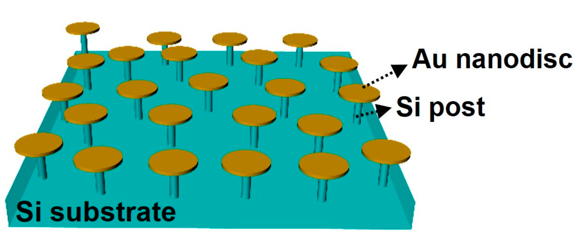
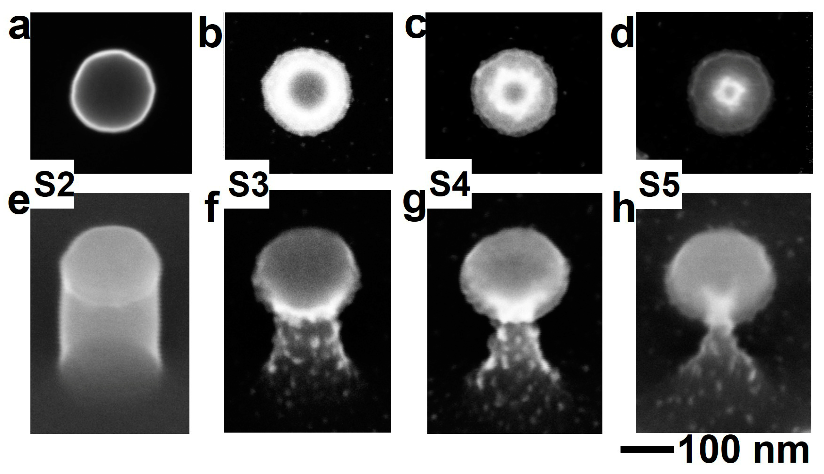
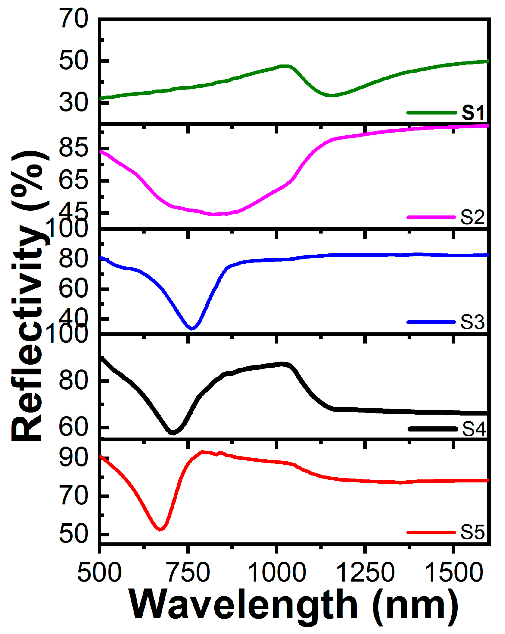
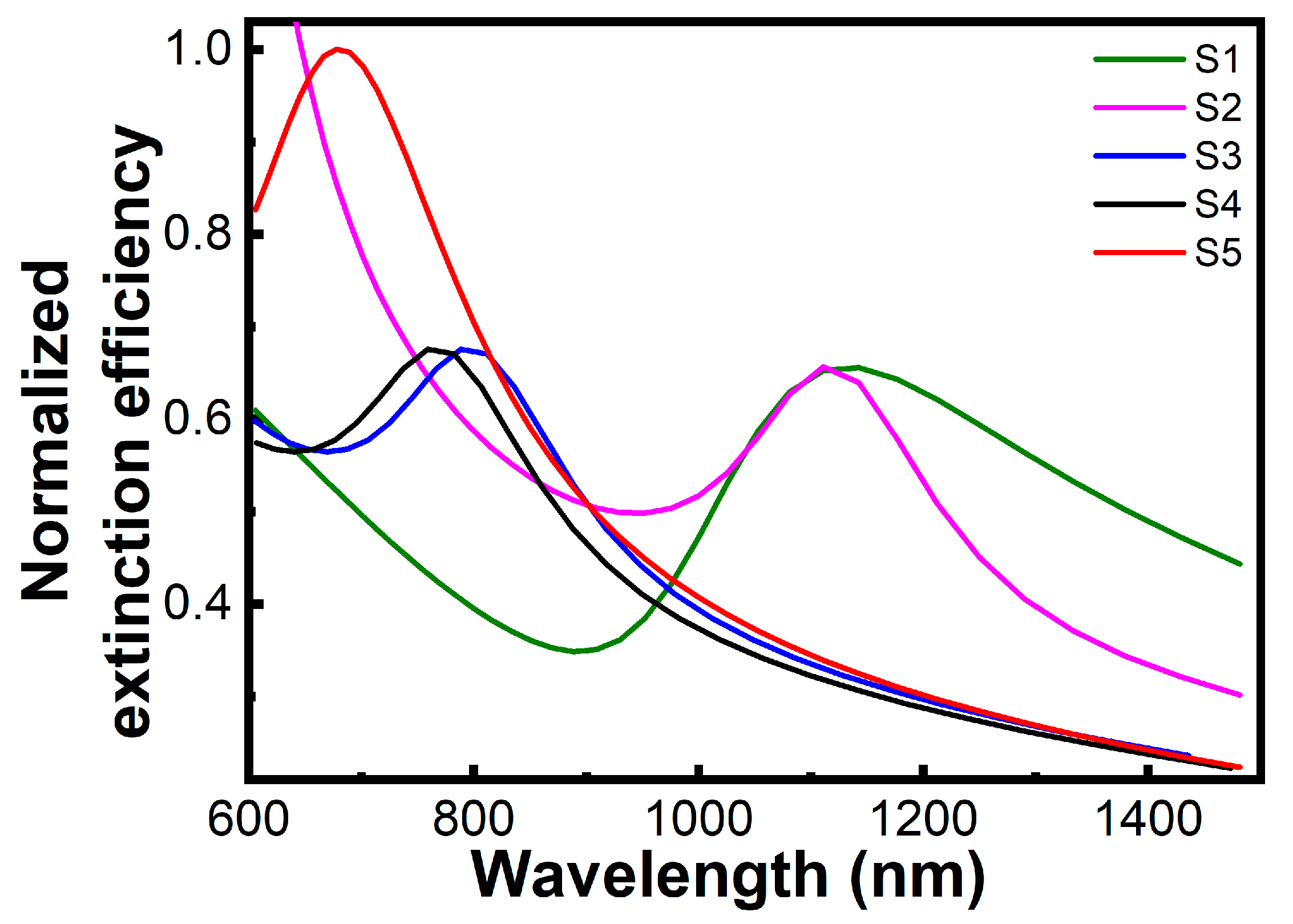
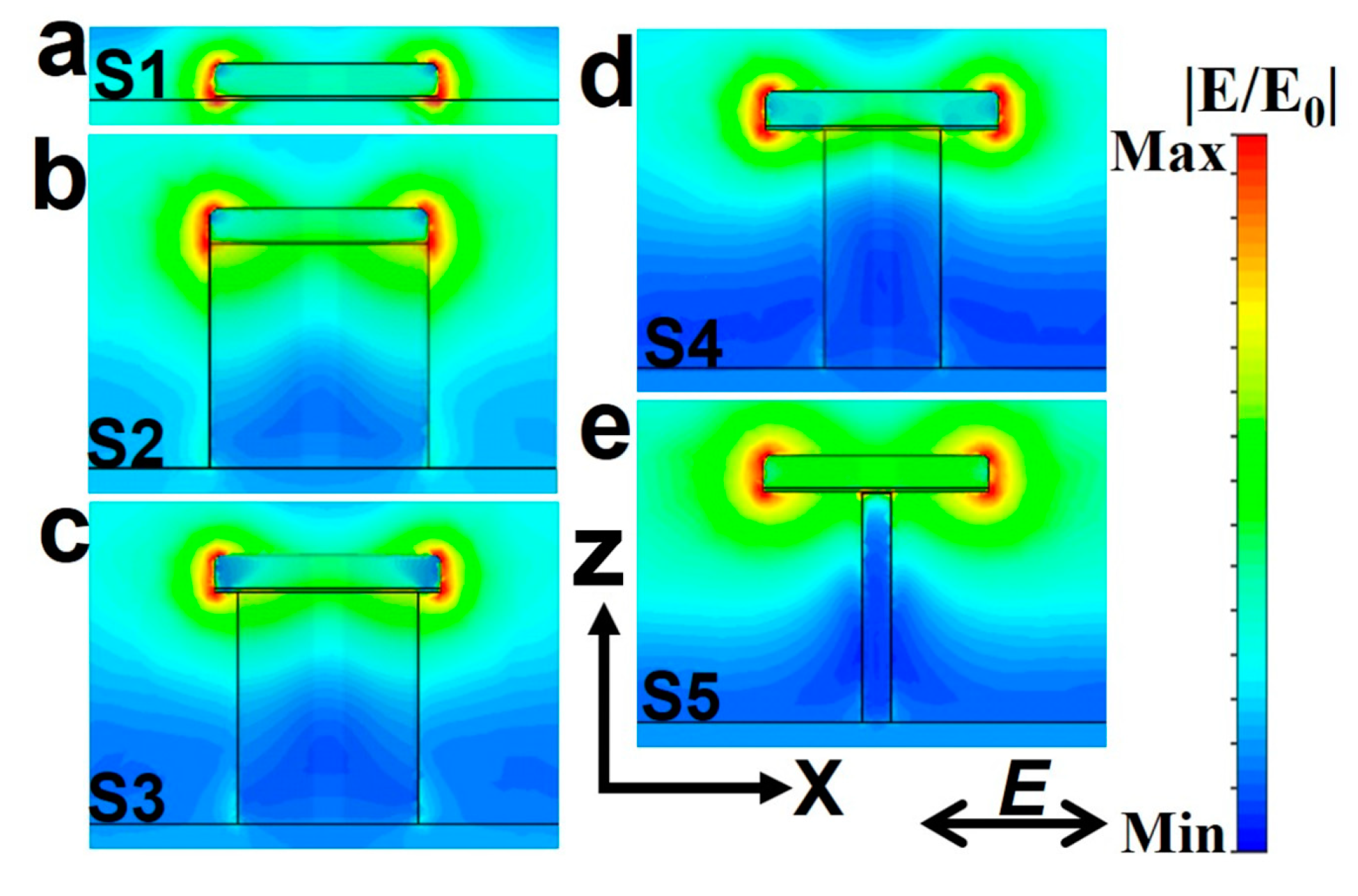
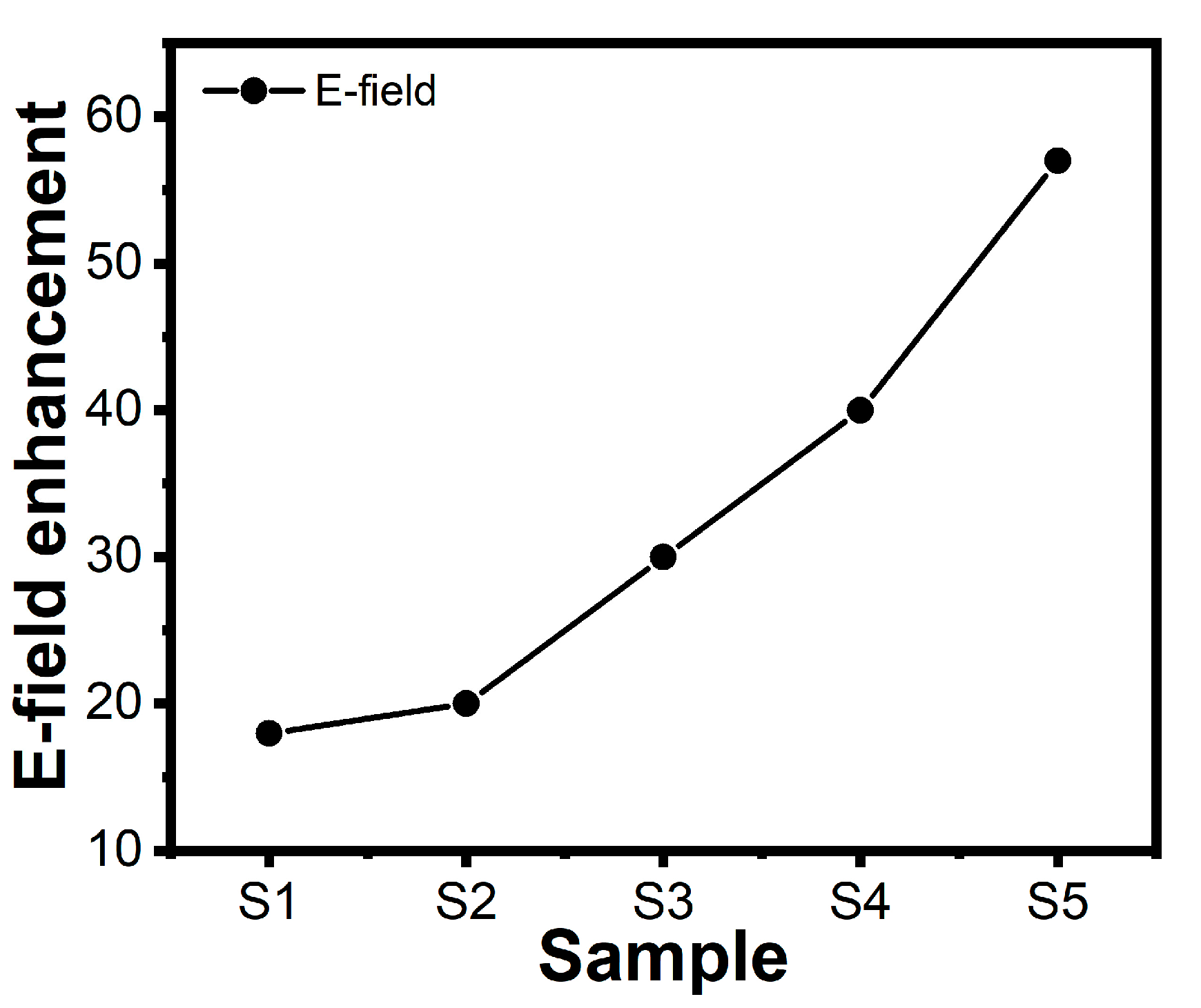
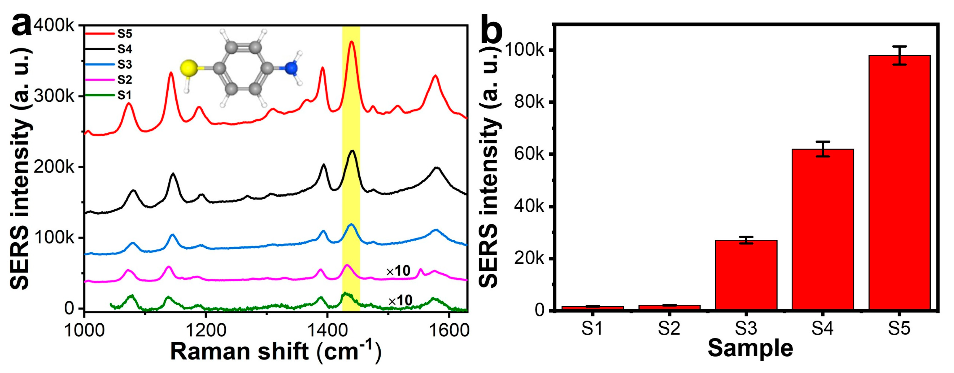
3. Results and Discussion

A schematic presentation of the formed pin-shaped nanostructures is shown in Figure 1. The diameter of the Au nanodisc is 160 nm, and the Si pillar diameter varies between 160 nm and 20 nm, while the height is kept constant at 150 nm for all produced structures. Table 1 presents the fabrication parameters used to shape the Si nanopillar supporting the Au disc. Sample S1 corresponds to the Au nanodisc formed on bulk Si. The samples with engineered posts are numbered from S2 to S5, indicating a decrease in the Si post (pillar) diameter. The corresponding SEM images are shown in Figure 2, where normal-incidence and tilted-view panels clearly show the pin-shaped nanostructures with various morphologies.
Figure 3 shows the reflectivity spectra of the nanostructures. For a 2D Au nanodisc formed on bulk Si (sample S1), the LSPR is located around a wavelength of 1145 nm, attributed to the high dielectric constant of silicon. In addition, a transition around 1100 nm is observed due to the indirect bandgap of the monocrystalline Si substrate [51]. When the Au nanodisc is elevated from the substrate by a Si pillar of 150 nm height, with a diameter identical to the Au disc (sample S2), the LSPR experiences a blue shift to 840 nm. This band overlaps with the reflection minima at lower wavelengths caused by Mie resonances originated by the silicon pillar [52,53,54], thus, leading to a decrease of reflection in a broad interval between approximately 600–1100 nm (spectrum S2 in Figure 3). By decreasing the silicon pillar diameter to 130 nm, while maintaining the nanostructure height at 150 nm, a further blueshift of the LSPR position to 760 nm is observed (sample S3). By decreasing the Si pillar diameter to 80 and 20 nm, while keeping the height at 150 nm (samples S4 and S5), the LSPR is shifted to 705 and 665 nm, respectively. Thus, upon decreasing the Si pillar diameter, a gradual blue shift of LSPR accompanied by a reduction of full width at half maximum (FWHM) of the band is observed.
To identify the origins of the LSPR modes and the reason for the observed blue shift, we conducted numerical simulations using the CST-FIT method. The spectra of the calculated extinction efficiency of the nanostructures, normalized to that of S5, are shown in Figure 4. Extinction efficiency is the ratio between the extinction cross section and the projected area of the nanostructure. The 2D Au nanodisc allocated on bulk Si exhibits LSPR at the wavelength of 1140 nm, providing a good agreement with the measured spectrum (see spectrum S1 in Figure 3). After raising the Au disc with a 150 nm pillar above the Si surface, the LSPR shifts to 1100 nm (spectrum S2 in Figure 4), while the band position was found to be around 840 nm in the measured spectrum (see Figure 3). This discrepancy could be related to deviations in the shapes of real 3D nanostructures from the ideal cylindrical morphology used in the simulations. It could also be that some produced pillars are etched to a diameter a bit smaller than 160 nm used in the simulations. However, a significant reduction of FWHM is observed, indicating a high Q-factored LSPR mode. After reducing the Si pillar diameter to 130, 80, and 20 nm, the calculated wavelengths of LSPRs closely match the experimentally observed ones (compare spectra S3, S4, and S5 in Figure 3 and Figure 4). The observed blue shift and band narrowing is caused by the decrease in effective dielectric constant at the metal-dielectric interface, resulting from the removal of silicon beneath the Au disc. Moreover, a significant improvement in extinction efficiency is observed for 3D pin structures with the smallest diameter of 20 nm when compared to 2D nanodiscs.
The electric field distributions originated by LSPR of the nanostructures in the x-z plane are shown in Figure 5, where E and E0 are the actual and initial electric fields. The respective enhancement factors (EF) of the samples are provided in Figure 6. The EF represents the maximum field localized at the hottest points of the hot spots. Electric field distributions clearly show a strong intensity increase at the edges of the nanodisc and indicate that these modes correspond to a dipolar LSPR. However, for the 2D nanostructure shown in Figure 5a, the hot spots at the interface with Si produce the field dissipating into the high-index substrate. Therefore, EF of such a plasmonic structure is not very high, 18 (see Figure 6). The 3D nanostructure with a 160 nm Si pillar diameter (Figure 5b) shows only a slight increase in EF to around 20 (Figure 6). This can be attributed to the lack of silicon removal beneath the Au nanodisc and a noticeable spatial overlap of the electric field produced by the nanodisc with the substrate. As the diameter of the Si pillar is gradually diminished to 130, 80, and 20 nm, the electric field enhancement, respectively, increases to 30, 40, and 57 (see Figure 6). The highest field enhancement was observed for an Si pillar with the smallest experimentally obtained contact area (20 nm diameter, 3D pin structure). In this case (Figure 5e), the field is confined to the edges of the nanodisc and does not interact with the high-index substrate, demonstrating successful decoupling of the hot spots from the substrate. Moreover, this strong field confined around the disc would highly affect the molecules which can be allocated in close vicinity (even beneath the disc) in the detection experiments. A further decrease of pillar diameter can lead to higher EF, but large-area production of 3D pin-shaped nanostructures with very thin posts would be a technological challenge affecting reproducibility.
Earlier publications have shown that the field enhancement can be increased by varying the nanostructure shape (cube, bowtie, or doughnut) while locating the structure on a pillar and elevating it from the bulk substrate [39,40,45,46]. Controlling the pillar height allowed to tune the plasmon resonance parameters and field enhancement. In this work, we suggest a novel approach, where the resonance conditions can be tuned by carving the substrate material beneath the 2D metallic nanostructure, thus, decreasing the interface area between the plasmonic structure and supporting pillar (changing the morphology into 3D). In this way, the resonance-induced EM field is decoupled from the substrate and the physical hot-spot interaction volume is increased. Varying the pillar diameter provides one more degree of freedom (additionally to change of pillar height) to tune the plasmon resonance conditions and the field enhancement factor.
The impact of decoupling the EM fields from the substrate on the sensing efficiency of the produced nanostructures is investigated experimentally using SERS. The SERS spectra of p-MA molecules chemisorbed from a solution with 1 μM concentration on S1-S5 samples are shown in Figure 7a. Raman modes typical for p-MA, centered at 1077, 1143, 1183, 1310, 1390, 1434, and 1577 cm−1, are discernible. The assignment of these modes to particular molecular vibrations can be found elsewhere [55,56,57]. An increase of intensity for all the above-mentioned modes is clearly observed with the Si pillar diameter decrease. Figure 7b illustrates this increase for one of the most prominent bands at 1434 cm−1. A 50× rise in SERS signal intensity is found for the pin-shaped structure with the smallest pillar diameter (sample S5) compared to the 2D discs formed on bulk Si (sample S1). The observed tendency is in good agreement with the electric field enhancement predicted by the simulations (Figure 6). Apart from the electric field enhancement due to a pin-shaped structure, the wavelength of LSPR for S5 is in line with the laser excitation wavelength; thereby, a high SERS signal intensity is obtained. The SERS EF of the 3D pin-shaped structures is calculated using the following expression, described elsewhere [58,59]:
E F = I S E R S I R a m a n × A R a m a n A S E R S × P R a m a n P S E R S × t S E R S t R a m a n
where I, A, P, and t are the peak intensity, the area of the Au nanodiscs, the laser power, and the accumulation time, respectively. The subscripts Raman and SERS stand for measurements taken on planar Au metal film and 3D structures, respectively. For SERS EF calculations, the incident power and accumulation time for both Raman and SERS measurements were kept constant. By considering 1μm laser illumination spot size, ARaman and ASERS were found to be 7.9 × 10⁻¹³ m2 and 3.9 × 10⁻¹⁶ m2, respectively, giving an ARaman/ASERS ratio of over 2000. The 3D pin-shaped structure provides an average SERS EF of 2 × 10⁶ obtained by evaluating the peak at 1434 cm−1.

4. Conclusions

In summary, we have investigated the substrate-mediated plasmonic response of Au nanodiscs. This study provided insight into the interaction of electric field produced in plasmon resonance with the dielectric substrate, shedding light on spectral shifts of LSPR and field enhancements. The 2D nanostructures formed on bulk dielectrics typically exhibit relatively low EM field enhancement due to strong field dissipation into the substrate. We have developed and experimentally verified an ability to tailor the LSPR of Au nanodiscs by fabricating pin-shaped nanostructures and engineering diameters of Si pillars supporting the discs. Decreasing the pillar diameter while keeping the same height and nanodisc size resulted in a higher hot-spot intensity. The simulations supported the observed LSPR spectral changes and the strong near-field enhancements. The nanodiscs supported by Si pillars of 20 nm in diameter demonstrated 3 times higher field enhancement compared to the similar nanodisc arrays on a bulk Si.
The plasmonic efficiency of the manufactured 3D pin-shaped nanostructures was tested in SERS measurements using p-MA as an analyte molecule. The 3D pin structures exhibited a SERS enhancement factor in the order of 106. On the one hand, the substrate-mediated LSPR enables strong hot spots, and on the other hand, the 3D geometry provides easier coupling of tested molecules to the plasmonic structures, thus, ensuring high enhancement factors of sensing. We anticipate that this work offers a promising platform for tuning the plasmon modes and amplifying the EM fields by decreasing the substrate influence, which is useful in many applications.

Author Contributions

Conceptualization, A.C. and V.N.P.; methodology, A.C., M.H.S., D.W., P.K.K. and D.S.S.; software, M.C.; validation, A.C.; formal analysis, A.C. and V.N.P.; investigation, A.C.; resources, K.P.; data curation, A.C.; writing—original draft preparation, A.C. and V.N.P.; writing—review and editing, A.C., M.C., V.N.P. and K.P.; visualization, M.C.; supervision, M.C. and V.N.P.; project administration, K.P.; funding acquisition, K.P. All authors have read and agreed to the published version of the manuscript.

Funding

This research received no external funding.

Institutional Review Board Statement

Not applicable.

Informed Consent Statement

Not applicable.

Data Availability Statement

All data are available from the authors upon reasonable request.

Conflicts of Interest

The authors declare no conflict of interest.

References

  1. Aćimović, S.S.; Kreuzer, M.P.; González, M.U.; Quidant, R. Plasmon Near-Field Coupling in Metal Dimers as a Step toward Single-Molecule Sensing. ACS Nano 2009, 3, 1231–1237. [Google Scholar] [CrossRef] [PubMed]
  2. Anker, J.N.; Hall, W.P.; Lyandres, O.; Shah, N.C.; Zhao, J.; Van Duyne, R.P. Biosensing with plasmonic nanosensors. Nat. Mater. 2008, 7, 442–453. [Google Scholar] [CrossRef] [PubMed]
  3. Jain, P.K.; El-Sayed, M.A. Noble Metal Nanoparticle Pairs: Effect of Medium for Enhanced Nanosensing. Nano Lett. 2008, 8, 4347–4352. [Google Scholar] [CrossRef]
  4. Lal, S.; Link, S.; Halas, N.J. Nano-optics from sensing to waveguiding. Nat. Photonics 2007, 1, 641–648. [Google Scholar] [CrossRef]
  5. Myroshnychenko, V.; Rodríguez-Fernández, J.; Pastoriza-Santos, I.; Funston, A.M.; Novo, C.; Mulvaney, P.; Liz-Marzán, L.M.; García de Abajo, F.J. Modelling the optical response of gold nanoparticles. Chem. Soc. Rev. 2008, 37, 1792–1805. [Google Scholar] [CrossRef] [Green Version]
  6. Chirumamilla, M.; Chirumamilla, A.; Yang, Y.; Roberts, A.S.; Kristensen, P.K.; Chaudhuri, K.; Boltasseva, A.; Sutherland, D.S.; Bozhevolnyi, S.I.; Pedersen, K. Large-Area Ultrabroadband Absorber for Solar Thermophotovoltaics Based on 3D Titanium Nitride Nanopillars. Adv. Opt. Mater. 2017, 5, 1700552. [Google Scholar] [CrossRef]
  7. Vernon, K.C.; Funston, A.M.; Novo, C.; Gómez, D.E.; Mulvaney, P.; Davis, T.J. Influence of Particle−Substrate Interaction on Localized Plasmon Resonances. Nano Lett. 2010, 10, 2080–2086. [Google Scholar] [CrossRef]
  8. Hu, M.; Novo, C.; Funston, A.; Wang, H.; Staleva, H.; Zou, S.; Mulvaney, P.; Xia, Y.; Hartland, G.V. Dark-field microscopy studies of single metal nanoparticles: Understanding the factors that influence the linewidth of the localized surface plasmon resonance. J. Mater. Chem. 2008, 18, 1949–1960. [Google Scholar] [CrossRef]
  9. Catchpole, K.R.; Polman, A. Design principles for particle plasmon enhanced solar cells. Appl. Phys. Lett. 2008, 93, 191113. [Google Scholar] [CrossRef] [Green Version]
  10. Das, G.; Chirumamilla, M.; Gopalakrishnan, A.; Toma, A.; Panaro, S.; Proietti Zaccaria, R.; De Angelis, F.; Di Fabrizio, E. Plasmonic nanostars for SERS application. Microelectron. Eng. 2013, 111, 247–250. [Google Scholar] [CrossRef]
  11. Hao, E.; Schatz, G.C. Electromagnetic fields around silver nanoparticles and dimers. J. Chem. Phys. 2003, 120, 357–366. [Google Scholar] [CrossRef]
  12. Schuller, J.A.; Barnard, E.S.; Cai, W.; Jun, Y.C.; White, J.S.; Brongersma, M.L. Plasmonics for extreme light concentration and manipulation. Nat. Mater. 2010, 9, 193–204. [Google Scholar] [CrossRef] [PubMed]
  13. Xu, C.; Ravi Anusuyadevi, P.; Aymonier, C.; Luque, R.; Marre, S. Nanostructured materials for photocatalysis. Chem. Soc. Rev. 2019, 48, 3868–3902. [Google Scholar] [CrossRef] [PubMed]
  14. Alabastri, A.; Toma, A.; Liberale, C.; Chirumamilla, M.; Giugni, A.; De Angelis, F.; Das, G.; Di Fabrizio, E.; Zaccaria, R.P. Interplay between electric and magnetic effect in adiabatic polaritonic systems. Opt. Express 2013, 21, 7538–7548. [Google Scholar] [CrossRef] [PubMed]
  15. Gopalakrishnan, A.; Malerba, M.; Tuccio, S.; Panaro, S.; Miele, E.; Chirumamilla, M.; Santoriello, S.; Dorigoni, C.; Giugni, A.; Proietti Zaccaria, R.; et al. Nanoplasmonic structures for biophotonic applications: SERS overview. Ann. Der Phys. 2012, 524, 620–636. [Google Scholar] [CrossRef]
  16. Lim, S.Y.; Hedrich, C.; Jiang, L.; Law, C.S.; Chirumamilla, M.; Abell, A.D.; Blick, R.H.; Zierold, R.; Santos, A. Harnessing Slow Light in Optoelectronically Engineered Nanoporous Photonic Crystals for Visible Light-Enhanced Photocatalysis. ACS Catal. 2021, 11, 12947–12962. [Google Scholar] [CrossRef]
  17. Li, S.; Miao, P.; Zhang, Y.; Wu, J.; Zhang, B.; Du, Y.; Han, X.; Sun, J.; Xu, P. Recent Advances in Plasmonic Nanostructures for Enhanced Photocatalysis and Electrocatalysis. Adv. Mater. 2021, 33, 2000086. [Google Scholar] [CrossRef]
  18. Cortés, E.; Wendisch, F.J.; Sortino, L.; Mancini, A.; Ezendam, S.; Saris, S.; de S. Menezes, L.; Tittl, A.; Ren, H.; Maier, S.A. Optical Metasurfaces for Energy Conversion. Chem. Rev. 2022, 122, 15082–15176. [Google Scholar] [CrossRef]
  19. Altug, H.; Oh, S.-H.; Maier, S.A.; Homola, J. Advances and applications of nanophotonic biosensors. Nat. Nanotechnol. 2022, 17, 5–16. [Google Scholar] [CrossRef]
  20. Sun, Y.; Lou, D.; Liu, W.; Zheng, Z.; Chen, X. SERS Labels for Optical Anticounterfeiting: Structure, Fabrication, and Performance. Adv. Opt. Mater. 2023, 11, 2201549. [Google Scholar] [CrossRef]
  21. Toma, A.; Das, G.; Chirumamilla, M.; Saeed, A.; Proietti Zaccaria, R.; Razzari, L.; Leoncini, M.; Liberale, C.; De Angelis, F.; Di Fabrizio, E. Fabrication and characterization of a nanoantenna-based Raman device for ultrasensitive spectroscopic applications. Microelectron. Eng. 2012, 98, 424–427. [Google Scholar] [CrossRef]
  22. Das, G.; Chirumamilla, M.; Toma, A.; Gopalakrishnan, A.; Zaccaria, R.P.; Alabastri, A.; Leoncini, M.; Di Fabrizio, E. Plasmon based biosensor for distinguishing different peptides mutation states. Sci. Rep. 2013, 3, 1792. [Google Scholar] [CrossRef] [Green Version]
  23. Chirumamilla, M.; Gopalakrishnan, A.; Toma, A.; Proietti Zaccaria, R.; Krahne, R. Plasmon resonance tuning in metal nanostars for surface enhanced Raman scattering. Nanotechnology 2014, 25, 235303. [Google Scholar] [CrossRef] [PubMed]
  24. Larsson, E.M.; Alegret, J.; Käll, M.; Sutherland, D.S. Sensing Characteristics of NIR Localized Surface Plasmon Resonances in Gold Nanorings for Application as Ultrasensitive Biosensors. Nano Lett. 2007, 7, 1256–1263. [Google Scholar] [CrossRef] [PubMed]
  25. Haynes, C.L.; Van Duyne, R.P. Nanosphere Lithography:  A Versatile Nanofabrication Tool for Studies of Size-Dependent Nanoparticle Optics. J. Phys. Chem. B 2001, 105, 5599–5611. [Google Scholar] [CrossRef]
  26. Kelly, K.L.; Coronado, E.; Zhao, L.L.; Schatz, G.C. The Optical Properties of Metal Nanoparticles:  The Influence of Size, Shape, and Dielectric Environment. J. Phys. Chem. B 2003, 107, 668–677. [Google Scholar] [CrossRef]
  27. Knight, M.W.; Wu, Y.; Lassiter, J.B.; Nordlander, P.; Halas, N.J. Substrates Matter: Influence of an Adjacent Dielectric on an Individual Plasmonic Nanoparticle. Nano Lett. 2009, 9, 2188–2192. [Google Scholar] [CrossRef]
  28. Forcherio, G.T.; Blake, P.; Seeram, M.; DeJarnette, D.; Roper, D.K. Coupled dipole plasmonics of nanoantennas in discontinuous, complex dielectric environments. J. Quant. Spectrosc. Radiat. Transf. 2015, 166, 93–101. [Google Scholar] [CrossRef] [Green Version]
  29. Hutter, T.; Elliott, S.R.; Mahajan, S. Interaction of metallic nanoparticles with dielectric substrates: Effect of optical constants. Nanotechnology 2013, 24, 035201. [Google Scholar] [CrossRef]
  30. Huck, C.; Toma, A.; Neubrech, F.; Chirumamilla, M.; Vogt, J.; De Angelis, F.; Pucci, A. Gold Nanoantennas on a Pedestal for Plasmonic Enhancement in the Infrared. ACS Photonics 2015, 2, 497–505. [Google Scholar] [CrossRef]
  31. Moritake, Y.; Tanaka, T. Impact of substrate etching on plasmonic elements and metamaterials: Preventing red shift and improving refractive index sensitivity. Opt. Express 2018, 26, 3674–3683. [Google Scholar] [CrossRef] [Green Version]
  32. Brian, B.; Sepúlveda, B.; Alaverdyan, Y.; Lechuga, L.M.; Käll, M. Sensitivity enhancement of nanoplasmonic sensors in low refractive index substrates. Opt. Express 2009, 17, 2015–2023. [Google Scholar] [CrossRef] [PubMed] [Green Version]
  33. Bauch, M.; Dostalek, J. Collective localized surface plasmons for high performance fluorescence biosensing. Opt. Express 2013, 21, 20470–20483. [Google Scholar] [CrossRef]
  34. Li, J.; Ye, J.; Chen, C.; Hermans, L.; Verellen, N.; Ryken, J.; Jans, H.; Van Roy, W.; Moshchalkov, V.V.; Lagae, L.; et al. Biosensing Using Diffractively Coupled Plasmonic Crystals: The Figure of Merit Revisited. Adv. Opt. Mater. 2015, 3, 176–181. [Google Scholar] [CrossRef]
  35. Hatab, N.A.; Hsueh, C.-H.; Gaddis, A.L.; Retterer, S.T.; Li, J.-H.; Eres, G.; Zhang, Z.; Gu, B. Free-Standing Optical Gold Bowtie Nanoantenna with Variable Gap Size for Enhanced Raman Spectroscopy. Nano Lett. 2010, 10, 4952–4955. [Google Scholar] [CrossRef] [PubMed]
  36. Shen, Y.; Zhou, J.; Liu, T.; Tao, Y.; Jiang, R.; Liu, M.; Xiao, G.; Zhu, J.; Zhou, Z.-K.; Wang, X.; et al. Plasmonic gold mushroom arrays with refractive index sensing figures of merit approaching the theoretical limit. Nat. Commun. 2013, 4, 2381. [Google Scholar] [CrossRef] [Green Version]
  37. Dmitriev, A.; Hägglund, C.; Chen, S.; Fredriksson, H.; Pakizeh, T.; Käll, M.; Sutherland, D.S. Enhanced Nanoplasmonic Optical Sensors with Reduced Substrate Effect. Nano Lett. 2008, 8, 3893–3898. [Google Scholar] [CrossRef]
  38. Chirumamilla, M.; Toma, A.; Gopalakrishnan, A.; Das, G.; Zaccaria, R.P.; Krahne, R.; Rondanina, E.; Leoncini, M.; Liberale, C.; De Angelis, F.; et al. 3D Nanostar Dimers with a Sub-10-nm Gap for Single-/Few-Molecule Surface-Enhanced Raman Scattering. Adv. Mater. 2014, 26, 2353–2358. [Google Scholar] [CrossRef]
  39. Cetin, A.E.; Etezadi, D.; Altug, H. Accessible Nearfields by Nanoantennas on Nanopedestals for Ultrasensitive Vibrational Spectroscopy. Adv. Opt. Mater. 2014, 2, 866–872. [Google Scholar] [CrossRef]
  40. Chen, H.; Bhuiya, A.M.; Liu, R.; Wasserman, D.M.; Toussaint, K.C., Jr. Design, Fabrication, and Characterization of Near-IR Gold Bowtie Nanoantenna Arrays. J. Phys. Chem. C 2014, 118, 20553–20558. [Google Scholar] [CrossRef]
  41. Otte, M.A.; Estévez, M.C.; Carrascosa, L.G.; González-Guerrero, A.B.; Lechuga, L.M.; Sepúlveda, B. Improved Biosensing Capability with Novel Suspended Nanodisks. J. Phys. Chem. C 2011, 115, 5344–5351. [Google Scholar] [CrossRef]
  42. Cara, E.; Mandrile, L.; Sacco, A.; Giovannozzi, A.M.; Rossi, A.M.; Celegato, F.; De Leo, N.; Hönicke, P.; Kayser, Y.; Beckhoff, B.; et al. Towards a traceable enhancement factor in surface-enhanced Raman spectroscopy. J. Mater. Chem. C 2020, 8, 16513–16519. [Google Scholar] [CrossRef]
  43. Pérez-Jiménez, A.I.; Lyu, D.; Lu, Z.; Liu, G.; Ren, B. Surface-enhanced Raman spectroscopy: Benefits, trade-offs and future developments. Chem. Sci. 2020, 11, 4563–4577. [Google Scholar] [CrossRef] [PubMed] [Green Version]
  44. Wang, X.; Huang, S.-C.; Hu, S.; Yan, S.; Ren, B. Fundamental understanding and applications of plasmon-enhanced Raman spectroscopy. Nat. Rev. Phys. 2020, 2, 253–271. [Google Scholar] [CrossRef]
  45. Du, Y.; Shi, L.; Hong, M.; Li, H.; Li, D.; Liu, M. A surface plasmon resonance biosensor based on gold nanoparticle array. Opt. Commun. 2013, 298–299, 232–236. [Google Scholar] [CrossRef]
  46. Xiong, X.; Clarke, D.; Lai, Y.; Bai, P.; Png, C.E.; Wu, L.; Hess, O. Substrate engineering of plasmonic nanocavity antenna modes. Opt. Express 2023, 31, 2345–2358. [Google Scholar] [CrossRef]
  47. Hanif, M.; Juluri, R.R.; Chirumamilla, M.; Popok, V.N. Poly(methyl methacrylate) composites with size-selected silver nanoparticles fabricated using cluster beam technique. J. Polym. Sci. Part B Polym. Phys. 2016, 54, 1152–1159. [Google Scholar] [CrossRef]
  48. Zamboni, F.; Makarevičiūtė, A.; Popok, V.N. Long-Term Plasmonic Stability of Copper Nanoparticles Produced by Gas-Phase Aggregation Method Followed by UV-Ozone Treatment. Appl. Nano 2022, 3, 102–111. [Google Scholar] [CrossRef]
  49. Fredriksson, H.; Alaverdyan, Y.; Dmitriev, A.; Langhammer, C.; Sutherland, D.S.; Zäch, M.; Kasemo, B. Hole–Mask Colloidal Lithography. Adv. Mater. 2007, 19, 4297–4302. [Google Scholar] [CrossRef]
  50. Palik, E.D. Handbook of Optical Constants of Solids; Academic Press: Cambridge, MA, USA, 1998; Volume 3. [Google Scholar]
  51. Kangsabanik, J.; Svendsen, M.K.; Taghizadeh, A.; Crovetto, A.; Thygesen, K.S. Indirect Band Gap Semiconductors for Thin-Film Photovoltaics: High-Throughput Calculation of Phonon-Assisted Absorption. J. Am. Chem. Soc. 2022, 144, 19872–19883. [Google Scholar] [CrossRef]
  52. Spinelli, P.; Verschuuren, M.A.; Polman, A. Broadband omnidirectional antireflection coating based on subwavelength surface Mie resonators. Nat. Commun. 2012, 3, 692. [Google Scholar] [CrossRef] [PubMed] [Green Version]
  53. Bezares, F.J.; Long, J.P.; Glembocki, O.J.; Guo, J.; Rendell, R.W.; Kasica, R.; Shirey, L.; Owrutsky, J.C.; Caldwell, J.D. Mie resonance-enhanced light absorption in periodic silicon nanopillar arrays. Opt. Express 2013, 21, 27587–27601. [Google Scholar] [CrossRef] [PubMed]
  54. Evlyukhin, A.B.; Eriksen, R.L.; Cheng, W.; Beermann, J.; Reinhardt, C.; Petrov, A.; Prorok, S.; Eich, M.; Chichkov, B.N.; Bozhevolnyi, S.I. Optical spectroscopy of single Si nanocylinders with magnetic and electric resonances. Sci. Rep. 2014, 4, 4126. [Google Scholar] [CrossRef] [PubMed] [Green Version]
  55. Gopalakrishnan, A.; Chirumamilla, M.; De Angelis, F.; Toma, A.; Zaccaria, R.P.; Krahne, R. Bimetallic 3D Nanostar Dimers in Ring Cavities: Recyclable and Robust Surface-Enhanced Raman Scattering Substrates for Signal Detection from Few Molecules. ACS Nano 2014, 8, 7986–7994. [Google Scholar] [CrossRef]
  56. Jackson, J.B.; Halas, N.J. Surface-enhanced Raman scattering on tunable plasmonic nanoparticle substrates. Proc. Natl. Acad. Sci. USA 2004, 101, 17930–17935. [Google Scholar] [CrossRef]
  57. Osawa, M.; Matsuda, N.; Yoshii, K.; Uchida, I. Charge transfer resonance Raman process in surface-enhanced Raman scattering from p-aminothiophenol adsorbed on silver: Herzberg-Teller contribution. J. Phys. Chem. 1994, 98, 12702–12707. [Google Scholar] [CrossRef]
  58. Chirumamilla, A.; Moise, I.-M.; Cai, Z.; Ding, F.; Jensen, K.B.; Wang, D.; Kristensen, P.K.; Jensen, L.R.; Fojan, P.; Popok, V.; et al. Lithography-free fabrication of scalable 3D nanopillars as ultrasensitive SERS substrates. Appl. Mater. Today 2023, 31, 101763. [Google Scholar] [CrossRef]
  59. Chirumamilla, M.; Chirumamilla, A.; Roberts, A.S.; Zaccaria, R.P.; De Angelis, F.; Kjær Kristensen, P.; Krahne, R.; Bozhevolnyi, S.I.; Pedersen, K.; Toma, A. Hot-Spot Engineering in 3D Multi-Branched Nanostructures: Ultrasensitive Substrates for Surface-Enhanced Raman Spectroscopy. Adv. Opt. Mater. 2017, 5, 1600836. [Google Scholar] [CrossRef]
Figure 1. Schematics of the 3D Au/Si nanopin-shaped structures.
Photonics 10 00821 g001
Figure 2. SEM images of (ad) top-view and (eh) 54° tilted-view of the manufactured nanostructures for various gas flow rates of SF6/C4F8 as provided in Table 1.
Photonics 10 00821 g002
Figure 3. Measured reflectivity spectra of produced nanostructures (samples S1–S5).
Photonics 10 00821 g003
Figure 4. Calculated extinction efficiency of the nanostructures equivalent to samples S1–S5. The extinction efficiency is normalized to that of S5.
Photonics 10 00821 g004
Figure 5. Electric (E) field distribution in the x–z plane of (ae) the nanostructures equivalent to samples S1–S5, respectively. The incident light is polarized along the x-direction.
Photonics 10 00821 g005
Figure 6. Calculated electric field enhancement for the structures equivalent to samples S1–S5.
Photonics 10 00821 g006
Figure 7. (a) SERS spectra of p-MA molecules (schematic structure is shown in inset) chemisorbed at 1 μM concentration on S1–S5 samples. (b) change of spectral line intensity at 1434 cm−1 for samples S1–S5. The excitation laser polarization was set along the x-axis, parallel to the substrate plane. For all SERS measurements, an incident laser power of 0.06 mW and an accumulation time of 10 s were used. The error bars illustrate the standard deviations of 10 measurements taken at random locations of each sample. The deviations are found to be less than 5%.
Photonics 10 00821 g007
Table 1. Etching parameters and corresponding Si pillar (post) diameters.
SampleSF6/C4F8
(SCCM)
Etching Time
(min)
Si Pillar Diameter
(nm)
S23/4060160
S311/6213130
S414/623.580
S525/75220
Disclaimer/Publisher’s Note: The statements, opinions and data contained in all publications are solely those of the individual author(s) and contributor(s) and not of MDPI and/or the editor(s). MDPI and/or the editor(s) disclaim responsibility for any injury to people or property resulting from any ideas, methods, instructions or products referred to in the content.

