Article

Design and Performance Analysis of the Highly Sensitive Deep Vacuum Cooling sCMOS Imaging System for Highly Sensitive Detection of Space Targets

1
Changchun Institute of Optics, Fine Mechanics and Physics, Chinese Academy of Sciences, Changchun 130033, China
2
University of Chinese Academy of Sciences, Beijing 100049, China
3
College of Communication Engineering, Jilin University, Changchun 130012, China
*
Author to whom correspondence should be addressed.
Photonics 2023, 10(7), 819; https://doi.org/10.3390/photonics10070819
Submission received: 26 May 2023 / Revised: 6 July 2023 / Accepted: 11 July 2023 / Published: 13 July 2023
(This article belongs to the Special Issue Optical Remote Sensor Design and Development)

Abstract

:
The sCMOS imaging system with deep vacuum cooling technology has become a necessary way to improve the detection capability of space targets. In order to improve the detection capability of the photoelectric detection equipment for space targets, this paper developed the Highly Sensitive Deep Vacuum Cooling Imaging System (HSDVCIS). Firstly, we designed the imaging readout processing circuit using the GSENSE4040 sCMOS image sensor designed and manufactured by Gpixel and the deep vacuum cooling structure using thermoelectric cooling. Then, we tested the designed HSDVCIS with readout noise, dark current, and dynamic range of 3.96 e , 0.12 e /pixel/sec, and 84.49 dB, respectively, and tested the image sensor with a minimum cooling temperature of −40 °C. Finally, according to the results of observation experiments, we validated that the photoelectric detection equipment equipped with HSDVCIS improved the limiting detection magnitude (at SNR = 5 level) from 13.22 to 13.51 magnitudes within a 3 s exposure time by turning on the cooling function. Therefore, HSDVCIS designed in this paper can achieve highly sensitive detection of space targets. At the same time, the development of HSDVCIS also provides technical reserves and strong support for future research on the imaging systems using multiple image sensor mosaics.

1. Introduction

According to the European Space Agency’s (ESA) annual Space Environment Report of 22 April 2022, the number of space targets in Earth orbit is increasing year by year and at an accelerating rate [1]. The monitoring of space targets is an important measure to protect the safe operation of spacecraft in orbit [2,3].
Scientific Complementary Metal Oxide Semiconductor (sCMOS) image sensors break through the technical bottleneck of high noise and low dynamic range of traditional Complementary Metal Oxide Semiconductor (CMOS) image sensors, and have gradually become the detector of choice for highly sensitive detection imaging systems for space targets [4,5]. At the same time, the use of deep vacuum cooling technology for sCMOS image sensors has become a necessary way to improve the detection capability of imaging systems for space targets. The number of photoelectric detection devices using deep vacuum cooling sCMOS imaging systems is currently increasing in the world.
The Kryoneri telescope in Greece is equipped with two thermoelectrically cooled Andor Zyla 5.5 sCMOS imaging systems [6,7]. This telescope achieves the limiting detection capability of 18.7 magnitudes in 10 s in both observing bands at the signal-to-noise ratio (SNR) level of 2.5. The Zimmerwald Laser and Astrometry Telescope (ZIMLAT) in Switzerland uses an sCMOS imaging system (Andor Neo) based on a vacuum-sealed cooling platform [8,9]. The Andor Neo has readout noise of 2 e and its image sensor can be cooled down to −40 °C by means of thermoelectric cooling and water-cooled heat dissipation. The Weizmann Fast Astronomical Survey Telescope (W-FAST) in Israel is equipped with a vacuum sealed sCMOS imaging system (Andor Balor) [10,11]. At the SNR level of 5, W-FAST has the limiting detection capability of 17.9 magnitudes in 3 s. The Panoptes-1AB telescope developed by the Baltic Institute of Technology (Baltech), and the Solaris-5 telescope, developed by the Polish Academy of Sciences, are equipped with a Kepler KL4040 sCMOS imaging system and a Kepler KL6060 sCMOS imaging system, respectively [12,13]. Both imaging systems are refrigerant cooled to −40 °C and −50 °C respectively. The Panoptes-1AB and Solaris-5 telescopes have limiting detection capability of 20.65 magnitudes and 22.54 magnitudes in 30 s, respectively, at the SNR level of 5.
Research on deep vacuum cooling sCMOS imaging systems has become a current hotspot for improving the detection capabilities of space target photoelectric detection equipment. In this paper, we developed the Highly Sensitive Deep Vacuum Cooling Imaging System (HSDVCIS) by designing the imaging readout processing circuit and the deep vacuum cooling structure. According to the performance tests and observation experiments conducted on HSDVCIS, the results validate that it can achieve highly sensitive detection of space targets.

2. Design of HSDVCIS

The circuit structure and external connections of HSDVCIS are shown in Figure 1. The overall structure of the imaging system consists of the Flexible High-speed LVDS (Low Voltage Differential Signaling) Transmission Path (FHSLTP), the High-speed Data Processing and Control Center (HSDPCC), the Thermoelectric Cooler (TEC), and the cooling fan. The imaging system is externally connected to the power supply equipment and the host computer, which act as the imaging system power supply and the data command interaction, respectively. In addition, the deep vacuum cooling structure ensures that the sCMOS image sensor cooling process is realized.
In this paper, the design of HSDVCIS is described in terms of the design of the imaging readout processing circuit and the design of the deep vacuum cooling structure.

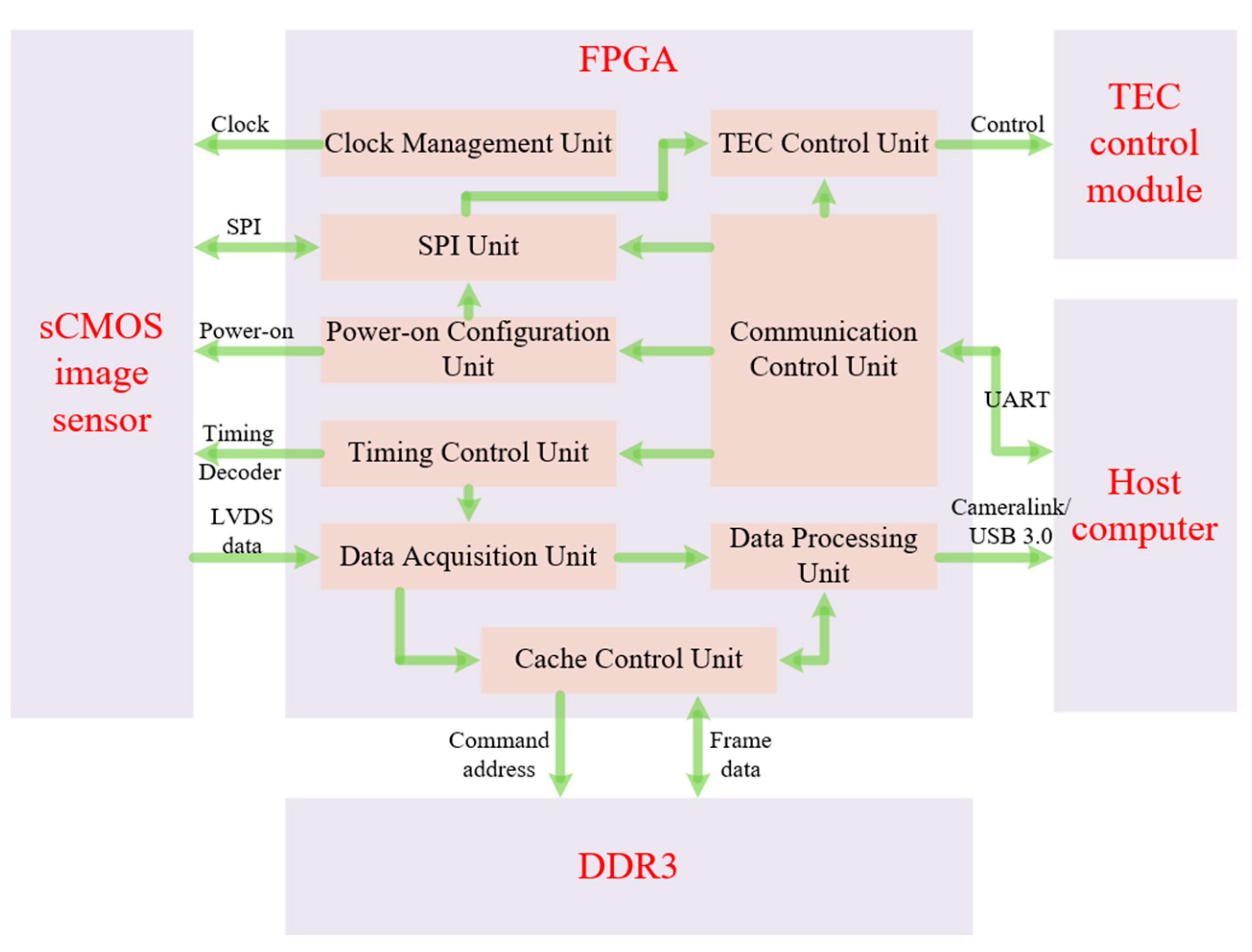
2.1. Design of the Imaging Readout Processing Circuit

2.1.1. Image Sensor Selection

The requirements for image sensors in space target detection applications are moving toward larger photosensitive area, higher resolution, larger pixel size, higher quantum efficiency, lower readout noise and dark current, etc. [14,15]. Compared with the image sensors developed by Andor, Fairchild, and other instrument companies, the relevant sCMOS image sensors developed by Gpixel in China for astronomical observation and scientific imaging applications are gradually attracting attention in related research fields due to their higher cost performance with basically the same performance parameters [16,17,18].
The relationship between the imaging area size of the optical system and its focal length and field of view is shown in Equation (1):
I = 2 f t a n ( ω 2 )
where I is the imaging area size of the optical system, f is the focal length of the optical system, and ω is the field of view of the optical system. When the horizontal field of view or vertical field of view is used as the parameter of Equation (1) for calculation, the dimensions of the calculated imaging area are the lengths in the horizontal and vertical directions, respectively.
According to Equation (1), in order to meet the full field of view imaging requirements of the photoelectric detection equipment with an aperture of 1005 mm, focal length of 1300 mm, field of view of 1.55° × 1.55°, and pixel scale of less than 1.5 arcsec/pixel, the image sensor of its imaging system shall have a photosensitive area of at least 35.17 mm × 35.17 mm and a resolution of at least 3720 × 3720. In this paper, we consider the requirements of image sensors for space target detection and satisfy the premise of meeting the above imaging requirements for the photoelectric detection equipment. At the same time, taking into account the cost of the imaging system, we finally selected the GSENSE4040 image sensor designed and manufactured by Gpixel as the core imaging element for the development of HSDVCIS. The main performance parameters of the GSENSE4040 image sensor are shown in Table 1. As can be seen from the table, the GSENSE4040 has good overall performance and is able to meet the above requirements for the image sensor.

2.1.2. Design of FHSLTP and HSDPCC

HSDVCIS is designed using the System on Programmable Chip (SOPC) approach, and the main logic functions of the whole system are performed by an FPGA chip. As shown in Figure 1, the imaging readout processing circuit of HSDVCIS consists of FHSLTP and HSDPCC.
FHSLTP serves as the communication link between the image sensor and HSDPCC for transmitting image data and drive control signals. HSDPCC is the heart of the imaging system, driving and controlling the various components of the system based on instructions from the host computer. It also processes the image data from FHSLTP and transmits them to the host computer for display.
The GSENSE4040 image sensor has 140 pins, 104 of which are used for image control and data transfer. The sensor generates the image data with a pixel depth of 12 bit and transmits them via 16 LVDS data pairs (DPs) at a data rate of up to 600 Mb/s. Therefore, in order to meet the drive control and data transmission requirements of the GSENSE4040 image sensor, the XC6SLX150-2FGG900C FPGA of the XILINX Spartan-6 series is used as the main control chip in this paper. The chip has strong logic processing capacity, with 6 I/O banks, a total of 576 I/Os, and 147,443 logic cells. It also has a differential I/O data transfer rate of up to 1080 Mb/s. Therefore, this FPGA is perfectly suited for the logic control and data sampling requirements of the image sensor.
As the core processor of HSDVCIS, the FPGA performs a large number of important logic functions, such as driving the GSENSE4040 sCMOS image sensor for proper operation, image data acquisition and processing, and image data upload. Figure 2 shows the block diagram of the logic function of the FPGA.
Communication control unit: The communication control unit performs the role of communication between the FPGA and the host computer, and is also the control center between each logic unit. The communication control unit receives and parses commands from the host computer, then drives the appropriate logic unit to operate, and finally returns the operating status to the host computer in the form of command frames.
Clock management unit: The clock management unit generates the clocks of different frequencies required by each component, such as the image sensor.
SPI (Serial Peripheral Interface) Unit: The SPI unit is the communication unit between the FPGA and the image sensor. The FPGA configures the relevant registers of the image sensor through the SPI unit. It implements Programmable Gain Amplifier (PGA) gain control, digital and analog linking, global pixel control, High Dynamic Range (HDR) mode selection, LVDS data output, and other functions.
Power-on configuration unit: The power-on configuration unit can avoid current peaks during powering on of the image sensor. Figure 3 shows the power-on configuration sequence of the image sensor. The power-on configuration unit generates the second set of power-enable signals, after the first set of power-enable signals is stabilized and the related configuration of the image sensor is completed.
Timing control unit: The timing control unit generates the drive signals for the image sensor exposure and readout, and controls the image exposure time and image readout mode. The timing control of the GSENSE4040 image sensor involves a total of 40 signals. Twenty-four of these signals are image sensor drive signals, and the other 16 are decoder signals. These decoder signals are used to control the row position of the image sensor for readout.
Data acquisition unit: The data acquisition unit receives the serial LVDS image data output from the image sensor and converts it to parallel 12-bit data. To ensure the accuracy of image data sampling by the data acquisition unit and to avoid data misalignment due to mismatch of LVDS output channels on the circuit system, the acquisition unit must perform alignment operations on the image data, including bit alignment, word alignment, and channel alignment. During alignment, the GSENSE4040 image sensor is in TRAINING mode. In this mode, it outputs fixed and known training words for sampling by the data acquisition unit. The data acquisition unit completes the data alignment operation by adjusting the sampling delay and comparing the differences between the sampled data and the training words. Figure 4 illustrates the LVDS image data alignment step, after which the data acquisition unit can correctly sample the data of each row in a frame.
Data processing unit: The data processing unit completes the appropriate processing of the image data and transfers the image data to the host computer by way of Cameralink or a USB3.0 interface. The appropriate processing mainly includes digital domain-related double sampling, high dynamic data synthesis, image pre-processing, and image output processing.
Cache control unit: The frame image data volume of the GSENSE4040 image sensor is 4096 × 4096 × 12 bit, approximately 192 Mb, and it cannot be directly processed in the frame buffer of the FPGA. The cache control unit controls the underlying operation of DDR3 using the IP core provided by XILINX. It uses the line-by-line reading and writing method to perform multiple operations on DDR, including reading and writing reset frame data, and reading and writing processed image frame data.
TEC control unit: The TEC control unit controls the operating state of the TEC by changing the enable signal of the TEC control module according to the difference between the image sensor temperature read by the SPI unit and the temperature set by the communication control unit.
Figure 5a,b show the physical diagrams of FHSLTP and HSDPCC, respectively. FHSLTP is designed using the flexible printed circuit (FPC) process and is able to penetrate the vacuum chamber with little or no effect on the chamber sealing. HSDPCC measures 86 mm × 90 mm; this is a small overall size that enables miniaturization of HSDVCIS. The digital and analog sections of HSDPCC are electrically isolated, thus reducing interference between digital and analog signals.

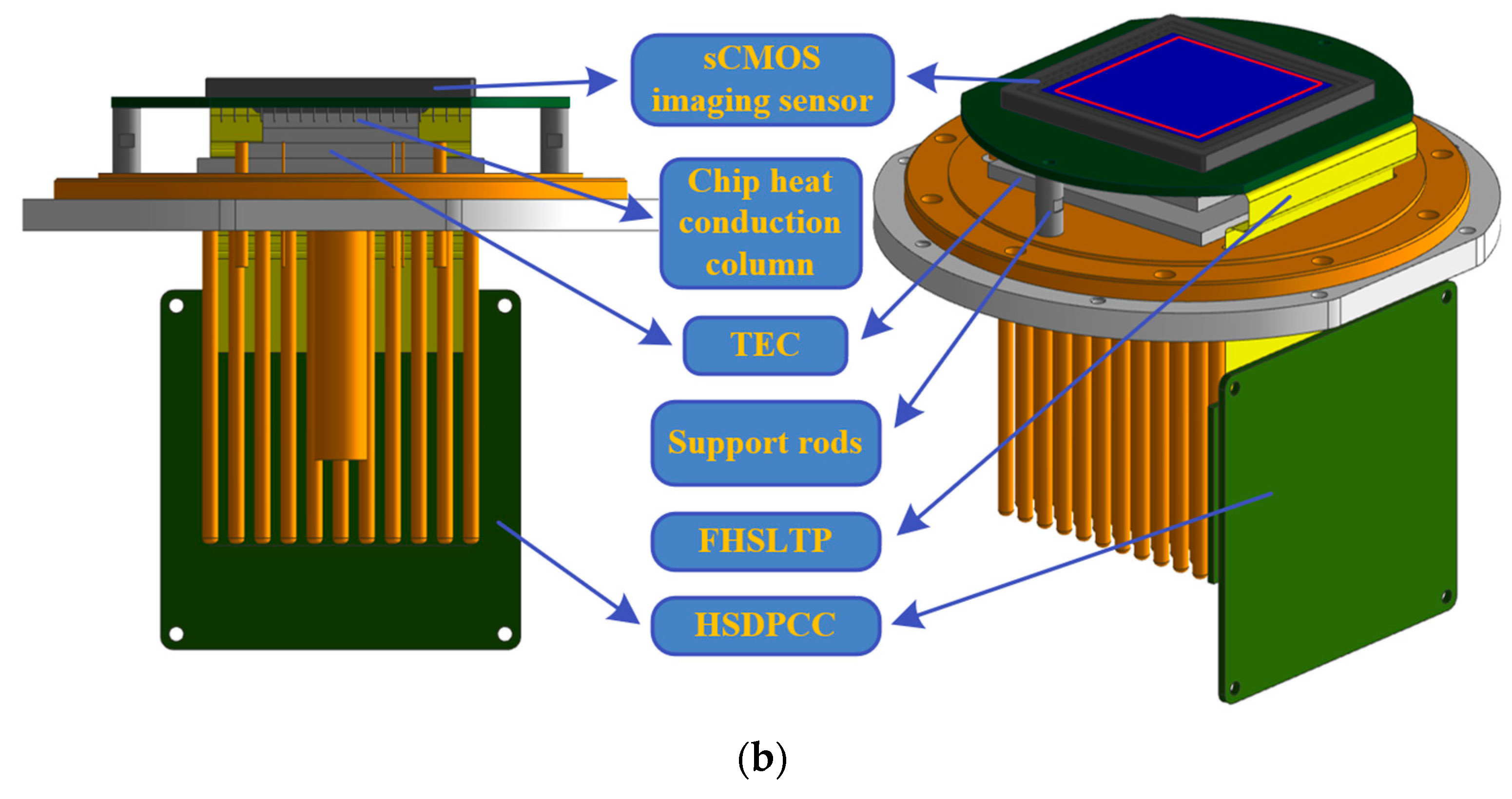
2.2. Design of the Deep Vacuum Cooling Structure

sCMOS image sensors are susceptible to moisture and other gaseous contaminants in atmospheric environments. Therefore, the image sensor must be vacuum encapsulated. Vacuum encapsulation not only protects the image sensor from erosion, but also reduces the heat exchange between the image sensor and the external environment, thus improving cooling performance. According to the relationship equation between the thermal conductivity of air and the vacuum degree in the literature [19], the relationship curve between the two is plotted as shown in Figure 6. When the vacuum degree is less than 10 2 Pa, the image sensor is considered to be negligibly affected by the heat exchange from the external environment.
The dark current of the sCMOS image sensor is strongly affected by temperature. Cooling is the most effective way to reduce the dark current. The main methods of image sensor cooling are refrigerant cooling, heat engine cooling, and thermoelectric cooling. TEC is a current transducer element that enables precise temperature control by controlling the input current. It requires no refrigerant, generates no vibration or noise during operation, and can be miniaturized for operation. TEC has clear advantages in the application of cooling to the image sensor [20,21]. Therefore, in this paper, the structure of HSDVCIS based on thermoelectric cooling is designed.
The deep vacuum cooling structure of HSDVCIS is shown in Figure 7. The yellow disk-shaped part in the figures is called the backshell, above which is the vacuum chamber. Inside the vacuum chamber are the sCMOS image sensor, the TEC, the FHSLTP, the chip heat conduction column, and the support rods. Below the backshell are the HSDPCC, the heatpipe set, the cooling fan, the evacuation copper tube and the support brackets. Parts such as the cooling fan and support brackets are not shown in Figure 7.
The image sensor is connected to the TEC through the chip heat conduction column with a high thermal conductivity. The TEC relies on the Peltier effect of semiconductor materials to cool the image sensor [22]. The hot end of the TEC is directly connected to the backshell so that the heat generated by the image sensor can be transferred through the backshell to the heatpipe set. The heat is then dissipated by thermal convection through the cooling fan. This completes the cooling of the image sensor.
The heatpipe set under the backshell is an 11 × 11 array of heatpipes. Each of these heatpipes is soldered to the back of the backshell and has a thermal conductivity of 680 W/(m∙K), which is nearly twice the thermal conductivity of copper. The design of the heatpipe set is perfectly matched to the heat transfer requirements of the image sensor during operation.
The air in the vacuum chamber can be evacuated using a vacuum pump connected to the evacuation copper tube. Before evacuating the air, the hole in the backshell for FHSLTP must be sealed. Since FHSLTP is designed using the FPC process, the sealing of the vacuum chamber will not be affected after the hole is sealed.

3. Performance Tests of HSDVCIS

The cooling performance of HSDVCIS designed in this paper was first tested. Within 10 min of turning on the cooling function of HSDVCIS, the temperature of the GSENSE4040 image sensor was measured to drop as low as −40 °C and remain stable by reading its built-in temperature sensor. HSDVCIS was then tested according to the EMVA1288 test standard [23] published by the European Machine Vision Association (EMVA) using the test platform consisting of an integrating sphere light source, darkroom, optical platform, and data acquisition console, as shown in Figure 8.
Readout noise and dark current are important parameters that affect the detection capability and image quality of the imaging system. In this paper, the readout noise and dark current of HSDVCIS were tested when the operating temperature of the image sensor was between −40 °C and 40 °C.
The readout noise test results of HSDVCIS at different temperatures of the image sensor are shown in Figure 9. It can be seen from Figure 9 that when the GSENSE4040 image sensor is operated from −40 °C to 40 °C, the readout noise of HSDVCIS fluctuates in the interval [3.9 e , 4.01 e ] and there is no functional relationship between the two. This indicates that the readout noise of the imaging system is not affected by the operating temperature of the image sensor. At the same time, the small fluctuation range of the readout noise (only 0.11 e ) indicates that the designed imaging readout processing circuit works stably. The readout noise fluctuation phenomenon of HSDVCIS is mainly caused by errors in the measurement process, such as small changes in the brightness of the integrating sphere light source and measurement curve fitting errors. Therefore, the effect of errors can be reduced by calculating the mean readout noise over multiple measurements. Based on the measured data in Figure 9, the mean readout noise of HSDVCIS can be calculated to be 3.96 e .
Figure 10 shows the results of the dark current test of HSDVCIS at different temperatures of the GSENSE4040 image sensor. The red line in the figure indicates the dark current of HSDVCIS measured by the dark field variance method, and the difference between the red lines at the two ends of the vertical axis is the measurement result. The blue line in the figure indicates the dark current of HSDVCIS measured by the dark field mean method, and the value of the vertical axis coordinate corresponding to each point of the blue line is the measurement result.
It is easy to see from the results of both methods that the dark current of HSDVCIS decreases significantly when the temperature of the image sensor is reduced from 40 °C to −40 °C. This is a direct indication that the deep vacuum cooling structure designed in this paper is effective in suppressing the dark current of the imaging system. According to the EMVA1288 test standard, the dark field mean method is more accurate for testing the dark current of imaging systems [23]. According to the test results of the dark field mean method, the dark current of HSDVCIS was reduced from 8.54 e /pixel/sec to 0.12 e /pixel/sec when the GSENSE4040 image sensor was cooled from room temperature (20 °C) to −40 °C. At this point, the dark current has a negligible effect on the detection capability and image quality of the imaging system.
According to the research related to the imaging systems of the several advanced photoelectric detection devices in this paper, it is found that the dark current of these imaging systems for space target detection applications reaches the order of 10 1   e /pixel/sec [8,11]. Therefore, in this paper, the dark current of HSDVCIS is suppressed to 0.12   e /pixel/sec by cooling the GSENSE4040 image sensor to −40 °C, thus meeting the requirement that the dark current of the imaging system for space target detection applications reaches the order of 10 1   e /pixel/sec.
Table 2 shows the test results of the main performance parameters of HSDVCIS. By comparing the performance parameters with the GSENSE4040 image sensor (i.e., Table 1 vs. Table 2), it is easy to see that the maximum frame rate of HSDVCIS is equal to the maximum frame rate of the image sensor. Meanwhile, the test results show that the readout noise and dynamic range of HSDVCIS are 3.96 e and 84.49 dB, respectively, which are basically the same as those parameters of the image sensor (readout noise and dynamic range are 3.7 e and 86 dB, respectively). This indicates that the design of the imaging readout processing circuit has little effect on the imaging of the image sensor and that HSDVCIS fully utilizes the performance of the GSENSE4040 image sensor.
Table 3 compares the main performance parameters of HSDVCIS designed in this paper with the Andor Zyla 5.5 imaging system of the Kryoneri telescope, the Andor Neo imaging system of the ZIMLAT, and the Kepler KL6060 imaging system of the Solaris-5 telescope. From the contents of Table 3, it can be seen that HSDVCIS has the lowest readout noise while satisfying the premise of large photosensitive area and large pixel size. In addition, HSDVCIS has higher resolution than Andor Zyla 5.5 and Andor Neo, so HSDVCIS generates more image data with the same pixel depth. This results in a lower maximum frame rate for HSDVCIS than for these two imaging systems, but it is still higher than the maximum frame rate of Kepler KL6060. Finally, the dynamic range of these four imaging systems differs relatively little. The above comparison shows that the overall performance of HSDVCIS designed in this paper is comparable to the performance level of several typical advanced highly sensitive imaging systems in the international arena.

4. Detection Capability Analysis and Validation

4.1. Theoretical Analysis

The detection capability of photoelectric detection equipment is usually measured in terms of SNR. The higher the SNR, the higher the magnitudes of the detected targets, i.e., the darker the target’s brightness. Empirically, SNR > 5 is considered as a robust criterion for reliable detection and extraction of space targets [24]. The smallest target magnitude observed by the photoelectric detection equipment at SNR = 5 is called the limiting detection magnitude for space targets. The limiting detection magnitude can also characterize the detection capability of the photoelectric detection equipment.
The SNR of the photoelectric detection equipment over the exposure time t i n t is expressed by Equation (2):
S N R = S M N 1 2 + N 2 2 + N 3 2 + σ R 2
where S M is the number of signal electrons generated by the target pixel during the exposure time t i n t , N 1 is the target photon noise, N 2 is the background photon noise, N 3 is the dark current noise of the imaging system, and σ R is the readout noise of the imaging system.
For a single target pixel, the number of signal electrons S M generated by the detection target within the exposure time t i n t is calculated as shown in Equation (3):
S M = P η = φ S η t i n t π D 2 τ a τ o ( 1 ε 2 ) 4 K
where P is the number of incident photons of the target (within the exposure time t i n t ), η is the quantum efficiency of the image sensor, φ S is the photon flux density of the target, D is the clear aperture of the optical system, τ a is the average transmittance of the atmosphere, τ o is the average transmittance of the optical system, ε is the obscuration ratio of the optical system, and K is the number of pixels occupied by the observed target in the image.
The φ S in Equation (3) corresponds to the photon flux density of the detection target of magnitude m V , which can be calculated by Equation (4):
φ S = φ 0 ( 2.512 ) m V
In the above equation, m V is the detection target magnitude, φ 0 is the photon flux density of the target of magnitude 0, and φ S is the photon flux density corresponding to the target of magnitude m V . φ 0 must be specified in order to calculate the limiting detection magnitude of the photoelectric detection equipment. According to the literature [25], assuming that the stellar radiation is blackbody radiation, the spectral photon flux density f ( λ ) at wavelength λ for various types of 0-magnitude stars can be calculated by Equation (5):
f ( λ ) = 8.48 × 10 34 × 10 0.4 m b T e 4 λ 4 [ E X P ( 1.44 × 10 8 λ T e ) 1 ]   ( p h o t o n s c m 2 s 1 1 )
where λ is the wavelength in Angstroms ( ), T e is the effective temperature of the star in Kelvin ( K ), and m b is the apparent bolometric magnitude of the star, a measure of the total energy output of the star. Using Equation (5), the spectral photon flux density curve of the solar spectrum at magnitude 0 can be plotted as shown in Figure 11. The effective temperature and apparent bolometric magnitude of the star are assumed to be of spectral type G2V. The value of φ 0 in Equation (4) is the integral of the spectral photon flux density of the 0-magnitude solar spectrum in the corresponding observed band.
The number of electrons S B produced by a background pixel during the exposure time t i n t is calculated as follows:
S B = B η = η t i n t h v π A d L B τ a τ 0 ( 1 ε 2 ) 4 F 2
where B is the number of incident photons from the skylight background during the exposure time t i n t , h is the Planck constant, v is the frequency of the electromagnetic wave, v = c / λ ¯ , where λ ¯ is the mean wavelength, c is the speed of light, L B is the skylight background irradiance, A d is the area of a single pixel of the image sensor, and F is the reciprocal of the relative aperture of the optical system.
The noise of the photoelectric detection equipment consists of four main components, namely target photon noise N 1 , background photon noise N 2 , dark current noise N 3 and readout noise σ R .
According to the relevant theory of quantum electrodynamics, the charge number of the photoelectric conversion follows a Poisson distribution [26,27]. Therefore, the target photon noise N 1 is equal to:
N 1 = f P η
where f is the super noise factor, which typically ranges from 1.0 to 1.4.
Similarly, the background photon noise N 2 is equal to:
N 2 = f B η
The dark current noise N 3 of the imaging system is equal to:
N 3 = f t i n t D e
where t i n t is the exposure time and D e is the dark current of the imaging system.

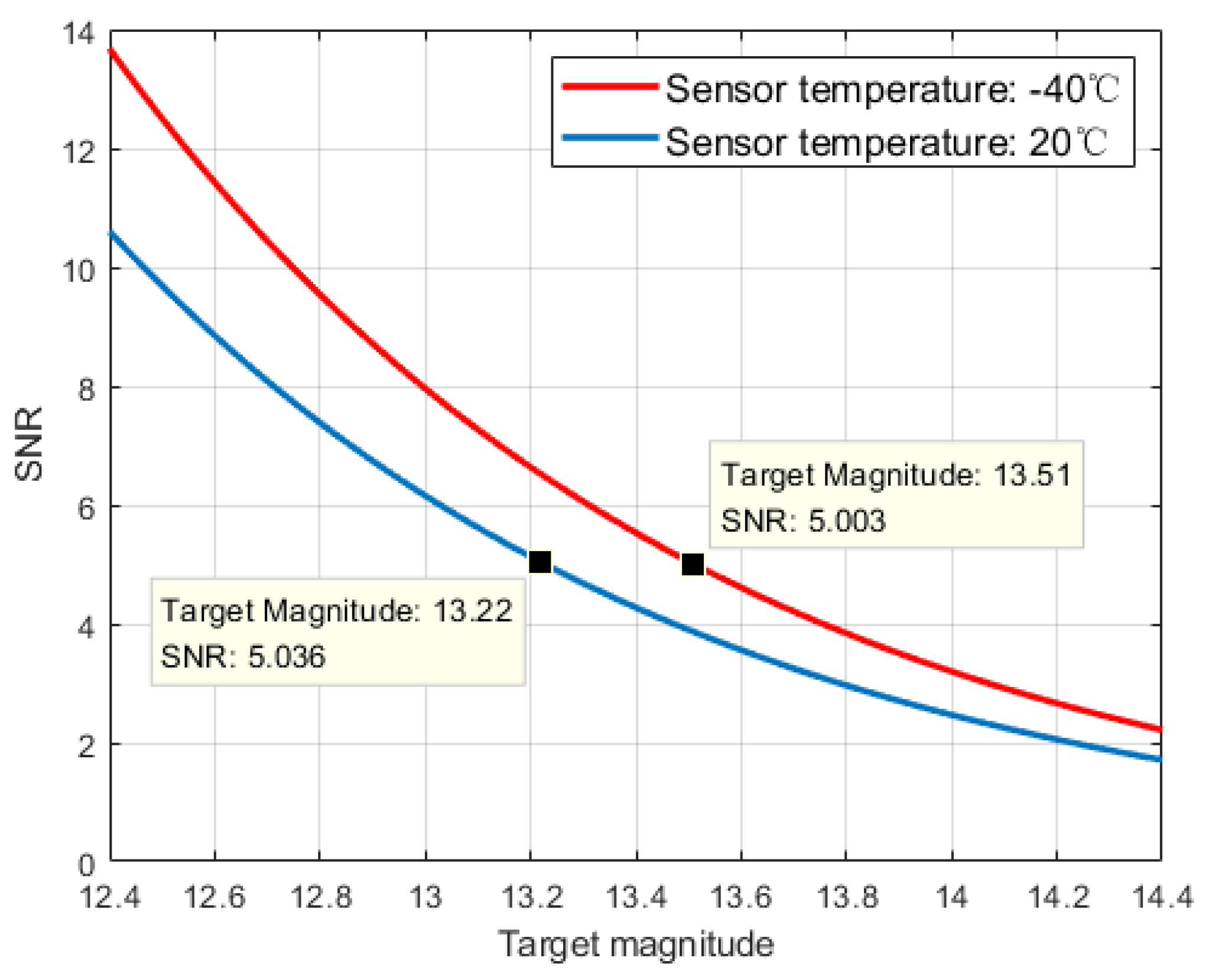
4.2. Experimental Validation

In order to validate the detection capability of the photoelectric detection equipment equipped with HSDVCIS, an optical observation platform as shown in Figure 12 was built in this paper.
The optical observation platform consists of three major components: HSDVCIS, the optical system, and the motion system. The main parameters of the optical system are listed in Table 4. The motion system has a range of 0° to 360° in the horizontal direction and an elevation angle of 0° to 90° in the vertical direction relative to the ground.
We used the optical observation platform to make imaging observation experiments in the suburbs of Changchun, China (longitude: 125°23′59″, latitude: 43°46′50″, altitude: 240 m, skylight background magnitude: 15 magnitudes). The observation point of the platform was set to the zenith direction (i.e., the observation elevation is set to 90°). When observing under this skylight background condition, setting HSDVCIS to the high-gain mode and the exposure time to 3 s allows it to achieve better linearity of the light response curve. At the same time, the operating temperature of the GSENSE4040 image sensor was set to 20 °C and −40 °C for observation experiments to validate the effectiveness of the designed deep vacuum cooling structure in improving the detection capability of HSDVCIS for space targets. No imaging parameters other than the image sensor temperature were changed in the observation experiments.
Firstly, we completely masked the entrance of the optical system in the optical observation platform so that HSDVCIS was in a dark field. This allowed us to observe more clearly the difference in the level of dark background noise in the images taken by HSDVCIS in both cases. For dark field imaging, HSDVCIS was also set to high-gain mode and the exposure time was set to 3 s. Figure 13 shows the dark field images taken by HSDVCIS under non-cooling and cooling conditions, the gray level distribution of the dark field images, and the gray histogram of the dark field images. Figure 13a,b are stretched to the same gray level interval when shown in the paper.
Observing Figure 13a, it is obvious that the image has a large amount of dark background noise. There are streak noise and a large number of single-pixel white shot noise dots in this image. When the image sensor is cooled to −40 °C, these two types of noise are barely visible in the image (as shown in Figure 13b). Figure 13c,d also show the dark background noise of the dark field images taken by HSDVCIS under non-cooling and cooling conditions. The points with a large gray level in Figure 13c are the large number of shot noise dots present in the corresponding image. Comparing these two images, it can be visually seen that the gray level of the dark field image taken by HSDVCIS under the cooling condition is more evenly distributed and the gray level mean is smaller. Figure 13e,f quantitatively show the difference between the dark field images taken by HSDVCIS in the two cases. The distribution of the gray histogram in Figure 13f is more concentrated. Comparing these two gray histograms, it is easy to see that the gray level mean and standard deviation of Figure 13a are much larger than those of Figure 13b. This is also visually reflected in the gray level distribution. From the above, it can be seen that the dark background noise in dark field images taken by HSDVCIS can be well suppressed by cooling the image sensor to −40 °C.
Next, we removed the mask at the entrance of the optical system so that the optical observation platform pointed toward the zenith for observation. The imaging conditions remain the same as previously described. The zenith images taken by HSDVCIS under non-cooling and cooling conditions are shown in Figure 14a,b. Neither image is dark subtracted, and both are stretched to the same gray level interval for display in the paper. Figure 14c shows the difference in the gray histogram of these two zenith images.
Comparing Figure 14a,b, it is easy to see that when the temperature of the image sensor is −40 °C, the zenith image taken by HSDVCIS has a darker background and a higher contrast between the background and the target. As can be seen from the details in these two images, Figure 14a has more background noise. It also has streak noise and a large number of single-pixel white shot noise dots. These noises, especially the shot noise dots, will affect the judgment and recognition of the target. It is easy to see from Figure 14c that by cooling the image sensor from 20 °C to −40 °C, the gray histogram of the image is distributed to the lower gray level and more centrally. The above shows that the zenith image taken by HSDVCIS under the cooling condition has a darker background and better image quality, and the noise in the image is effectively suppressed.
Finally, according to the calculation of Equations (2)–(9), and the relevant classification methods of image morphology, the detection capability curves of the optical observation platform can be calculated and plotted for the non-cooling and cooling conditions, respectively. The curves are shown in Figure 15.
According to the previous section and based on the detection capability curve in Figure 15, it can be easily seen that when the operating temperature of the GSENSE4040 image sensor is 20 °C, the photoelectric detection equipment with HSDVCIS has a limiting detection magnitude (at SNR = 5 level) of 13.22 magnitudes within a 3 s exposure time. When the image sensor is cooled to −40 °C, the limiting detection magnitude (at SNR = 5 level) of the photoelectric detection equipment increases to 13.51 magnitudes under the same conditions. As a result, under the set observation conditions and imaging parameters, the deep vacuum cooling of the GSENSE4040 image sensor has increased the limiting detection magnitude of the photoelectric detection equipment equipped with HSDVCIS by 0.29 magnitudes, i.e., the brightness of the faintest target can be detected when approximately 1.306 times fainter compared to the non-cooling condition.

5. Discussion

According to the results of the performance test experiments, the readout noise, dark current, and dynamic range of HSDVCIS are 3.96 e , 0.12 e /pixel/sec, and 84.49 dB, respectively, and the minimum cooling temperature of the image sensor is −40 °C. The dark current of HSDVCIS can reach the order of 10 1   e /pixel/sec, which meets the dark current requirement of the imaging system for space target detection applications. Comparing the performance parameters of HSDVCIS and the GSENSE4040 image sensor, we found that the maximum frame rate, readout noise, and dynamic range of the two are basically the same. This indicates that the imaging readout processing circuit of HSDVCIS has little effect on the imaging of the GSENSE4040 image sensor, which fully utilizes its performance. By comparing the performance parameters of HSDVCIS with several typical international advanced highly sensitive imaging systems, the results show that the overall performance of HSDVCIS is comparable to the performance level of these imaging systems.
The results of the observation experiments visually show that the quality of the images taken by HSDVCIS under the cooling condition (image sensor operating temperature: −40 °C) is much better than that of the images taken under the non-cooling condition (image sensor operating temperature: 20 °C). This shows that the deep vacuum cooling structure of HSDVCIS is very effective in suppressing the background noise during the imaging process and significantly improving the image quality. On this basis, through the calculation and analysis of the detection capability of the optical observation platform, its limiting detection magnitude (at SNR = 5 level) in a 3 s exposure time reaches 13.51 magnitudes, which is 0.29 magnitudes higher than the limiting detection magnitude (at SNR = 5 level) when the image sensor is not cooled. This quantitatively demonstrates that the designed deep vacuum cooling structure can effectively improve the detection capability of HSDVCIS.
According to the relevant formula for calculating the SNR of photoelectric detection equipment, the dark current noise is only a part of the calculation of limiting detection magnitude. The detection capability of the photoelectric detection equipment is also affected by the brightness of the skylight background, the aperture and focal length of the optical system, and many other factors. Therefore, the improvement appears to be relatively insignificant in terms of the value of the limiting detection magnitude. However, the deep vacuum cooling structure designed in this paper can significantly improve the image quality of HSDVCIS. The higher image quality facilitates subsequent operations such as the judgment and recognition of the targets in the image.
The research and design of the HSDVCIS in this paper, as well as the good test results achieved, will provide technical reserves and strong support for the future research of using 4 × 4 or more GSENSE4040 image sensor mosaics, so as to achieve a larger photosensitive area and higher-resolution imaging system.

6. Conclusions

In order to improve the detection capability of the photoelectric detection equipment for space targets, this paper developed HSDVCIS by designing the imaging readout processing circuit and the deep vacuum cooling structure. Based on the results of performance test experiments and observation experiments, it is proven that HSDVCIS designed in this paper is suitable for achieving highly sensitive detection of space targets.

Author Contributions

Conceptualization, Z.W., T.C., M.S. and C.L. (Changzheng Lu); methodology, C.L. (Changzheng Lu), C.L. (Changhua Liu) and J.C.; software, C.L. (Changzheng Lu), M.S. and C.J.; validation, C.L. (Changzheng Lu), C.J. and J.C.; formal analysis, C.L. (Changzheng Lu), C.L. (Changhua Liu), C.J. and J.C.; investigation, C.L. (Changzheng Lu) and C.J.; data curation, C.L. (Changzheng Lu) and C.J.; writing—original draft preparation, C.L. (Changzheng Lu); writing—review and editing, M.S., C.L. (Changzheng Lu), C.L. (Changhua Liu), Z.W. and C.J.; visualization, C.L. (Changzheng Lu), C.L. (Changhua Liu) and M.S.; supervision, Z.W. and T.C.; project administration, Z.W., T.C. and C.L. (Changhua Liu); funding acquisition, C.L. (Changhua Liu). All authors have read and agreed to the published version of the manuscript.

Funding

This research was funded by the National Key Research and Development Program of China, grant number 2020YFA0406502.

Institutional Review Board Statement

Not applicable.

Informed Consent Statement

Not applicable.

Data Availability Statement

Not applicable.

Acknowledgments

The authors are very grateful to the Changchun Changguang Orion Optoelectronic Technology Co., Ltd. for providing the EMVA1288 test platform for this paper, and to everyone at the company for their help in testing the imaging system.

Conflicts of Interest

The authors declare no conflict of interest.

References

  1. ESA Space Debris Office. ESA’s Annual Space Environment Report; ESA: Darmstadt, Germany, 2022. [Google Scholar]
  2. Schildknecht, T. Optical surveys for space debris. Astron. Astrophys. Rev. 2007, 14, 41–111. [Google Scholar] [CrossRef] [Green Version]
  3. Rubenchik, A.M.; Fedoruk, M.P.; Turitsyn, S.K. The effect of self-focusing on laser space-debris cleaning. Light Sci. Appl. 2014, 3, e159. [Google Scholar] [CrossRef] [Green Version]
  4. Karpov, S.; Bajat, A.; Christov, A.; Prouza, M.; Beskin, G. Evaluation of scientific CMOS sensors for sky survey applications. In Proceedings of the SPIE 11454, X-ray, Optical, and Infrared Detectors for Astronomy IX, 114540G, Online Only, 14–18 December 2020; pp. 86–98. [Google Scholar] [CrossRef]
  5. Wu, Y.; Sharma, M.K.; Veeraraghavan, A. WISH: Wavefront imaging sensor with high resolution. Light Sci. Appl. 2019, 8, 44. [Google Scholar] [CrossRef] [PubMed] [Green Version]
  6. Bonanos, A.; Xilouris, M.; Boumis, P.; Bellas-Velidis, I.; Maroussis, A.; Dapergolas, A.; Fytsilis, A.; Charmandaris, V.; Tsiganis, K.; Tsinganos, K. NELIOTA: ESA’s new NEO lunar impact monitoring project with the 1.2 m telescope at the National Observatory of Athens. Proc. Int. Astron. Union 2015, 10, 327–329. [Google Scholar] [CrossRef]
  7. Xilouris, E.M.; Bonanos, A.Z.; Bellas-Velidis, I.; Boumis, P.; Dapergolas, A.; Maroussis, A.; Liakos, A.; Alikakos, I.; Charmandaris, V.; Dimou, G.; et al. NELIOTA: The wide-field, high-cadence, lunar monitoring system at the prime focus of the Kryoneri telescope. Astron. Astrophys. 2018, 619, A141. [Google Scholar] [CrossRef] [Green Version]
  8. Ploner, M.; Lauber, P.; Prohaska, M.; Schlatter, P.; Utzinger, J.; Schildknecht, T.; Jäggi, A. The new CMOS Tracking Camera used at the Zimmerwald Observatory. In Proceedings of the 18th International Workshop on Laser Ranging, Fujiyoshida, Japan, 11–15 November 2013. [Google Scholar]
  9. Silha, J.; Linder, E.; Hager, M.; Schildknecht, T. Optical light curve observations to determine attitude states of space debris. In Proceedings of the 30th International Symposium on Space Technology and Science, Kobe-Hyogo, Japan, 3–9 June 2015. [Google Scholar]
  10. Nir, G.; Ofek, E.O.; Ben-Ami, S.; Manulis, I.; Gal-Yam, A.; Diner, O.; Rappaport, M. Weizmann Fast Astronomical Survey Telescope (WFAST). In Proceedings of the American Astronomical Society Meeting Abstracts# 229, Grapevine, TX, USA, 3–7 January 2017. id. 155.06. [Google Scholar]
  11. Nir, G.; Ofek, E.O.; Ben-Ami, S.; Segev, N.; Polishook, D.; Hershko, O.; Diner, O.; Manulis, I.; Zackay, B.; Gal-Yam, A.; et al. The Weizmann Fast Astronomical Survey Telescope (W-FAST): System Overview. Publ. Astron. Soc. Pac. 2021, 133, 075002. [Google Scholar] [CrossRef]
  12. Polkowska, M.; Chimicz, A. Status of SSA activities in Poland and recent SST developments. J. Space Saf. Eng. 2022, 9, 629–635. [Google Scholar] [CrossRef]
  13. Rogowska, B.; Konacki, M.; Chimicz, A.; Pawłaszek, R.; Kozłowski, S.; Sybilski, P.; Zwyciestwa, A. Panoptes-1AB and Solaris-5 unique wide field telescopes with sCMOS cameras. In Proceedings of the Advanced Maui Optical and Space Surveillance Technologies Conference, Maui, HI, USA, 17–20 September 2019; p. 75. [Google Scholar]
  14. Farrell, J.; Xiao, F.; Kavusi, S. Resolution and light sensitivity tradeoff with pixel size. In Proceedings of the SPIE 6069, Digital Photography II, 60690N, San Jose, CA, USA, 15–19 January 2006; pp. 211–218. [Google Scholar] [CrossRef]
  15. Minoglou, K.; Nelms, N.; Ciapponi, A.; Weber, H.; Wittig, S.; Leone, B.; Crouzet, P. Infrared image sensor developments supported by the European Space Agency. Infrared Phys. Technol. 2019, 96, 351–360. [Google Scholar] [CrossRef]
  16. Gill, A.S.; Shaaban, M.M.; Tohuvavohu, A.; Sivanandam, S.; Abraham, R.G.; Chen, S.; Drout, M.R.; Lokhorst, D.; Matzner, C.D.; Mochnacki, S.W. A low-cost ultraviolet-to-infrared absolute quantum efficiency characterization system of detectors. In Proceedings of the SPIE 12191, X-ray, Optical, and Infrared Detectors for Astronomy X, 1219114, Montréal, QC, Canada, 17–23 July 2022; pp. 374–388. [Google Scholar] [CrossRef]
  17. Ma, K.; Shi, Z.; Wang, H.; Zou, J.; Wang, W. A research on non-uniformity index of star sensor based on CMOS. In Proceedings of the SPIE 11763, Seventh Symposium on Novel Photoelectronic Detection Technology and Applications, 1176387, Kunming, China, 5–7 November 2020; pp. 2165–2171. [Google Scholar] [CrossRef]
  18. Yao, P.; Zhu, B.; Li, C.; Wang, H.; Dai, H.; Yang, Y. Design of solar observation electronics system for space application. In Proceedings of the SPIE 12069, AOPC 2021: Novel Technologies and Instruments for Astronomical Multi-Band Observations, 120690T, Beijing, China, 23–25 July 2021; pp. 184–189. [Google Scholar] [CrossRef]
  19. Huang, Z.-g.; Xu, Y.-l.; Wang, J.-m.; Zhang, Y.; Chen, C.; Zhang, H.-f.; Wang, J. Thermodynamics simulation for vacuum head of a 1K x 1K CCD camera. In Proceedings of the SPIE 10709, High Energy, Optical, and Infrared Detectors for Astronomy VIII, 107092J, Austin, TX, USA, 10–15 June 2018; pp. 626–631. [Google Scholar] [CrossRef]
  20. He, J.; Tritt, T.M. Advances in thermoelectric materials research: Looking back and moving forward. Science 2017, 357, eaak9997. [Google Scholar] [CrossRef] [PubMed] [Green Version]
  21. Pan, C.; Youshan, Q.; Huijuan, L.; Jiahai, T. Design and implementation of cooling system for focal plane assembly of observation camera in astronomical satellite. In Proceedings of the 2011 International Conference on Electronics, Communications and Control (ICECC), Ningbo, China, 9–11 September 2011; pp. 2615–2619. [Google Scholar]
  22. Yu, Y.; Zhu, W.; Kong, X.; Wang, Y.; Zhu, P.; Deng, Y. Recent development and application of thin-film thermoelectric cooler. Front. Chem. Sci. Eng. 2020, 14, 492–503. [Google Scholar] [CrossRef]
  23. EMVA 1288; Standard for Characterization of Image Sensors and Cameras. European Machine Vision Association: Barcelona, Spain, 2016; Release 3.1.
  24. Torralba, O.R.; Jehn, R.; Koschny, D.; Frühauf, M.; Jehn, L.S.; Praus, A. Simulation of Sky Surveys with the Flyeye telescope. arXiv 2019, arXiv:1903.08413. [Google Scholar]
  25. Zombeck, M.V. Handbook of Space Astronomy and Astrophysics; Cambridge University Press: Cambridge, UK, 2006. [Google Scholar]
  26. Jin, X.; Hirakawa, K. Approximations to camera sensor noise. In Proceedings of the SPIE 8655, Image Processing: Algorithms and Systems XI, 86550H, Burlingame, CA, USA, 3–7 February 2013; pp. 149–155. [Google Scholar] [CrossRef]
  27. Pan, Y.; Fan, X.; Wang, H.; Zhao, H.; Qiu, Y.; Gao, W.; Zhang, J. Accurate Determination of Conversion Gains of SVOM VT CCDs Based on a Signal-Dependent Charge-Sharing Mechanism. Electronics 2021, 10, 931. [Google Scholar] [CrossRef]
Figure 1. Block diagram of the circuit structure and external connections of HSDVCIS.
Photonics 10 00819 g001
Figure 2. Logic function block diagram of the FPGA.
Photonics 10 00819 g002
Figure 3. Power-on configuration sequence of the image sensor.
Photonics 10 00819 g003
Figure 4. LVDS image data alignment steps: (a) before alignment; (b) after bit alignment; (c) after word alignment; (d) after channel alignment. (A square with a number represents 1-bit data in the training word, and training words sent in sequence are distinguished by different colors.)
Photonics 10 00819 g004
Figure 5. Physical diagrams of the imaging readout processing circuit of HSDVCIS: (a) FHSLTP; (b) HSDPCC.
Photonics 10 00819 g005
Figure 6. Curve between thermal conductivity of air and vacuum degree.
Photonics 10 00819 g006
Figure 7. Design schemes of the deep vacuum cooling structure of HSDVCIS: (a) the deep vacuum cooling structure of HSDVCIS; (b) the internal structure of the vacuum chamber of HSDVCIS.
Photonics 10 00819 g007aPhotonics 10 00819 g007b
Figure 8. Imaging system performance test platform.
Photonics 10 00819 g008
Figure 9. Results of the HSDVCIS readout noise test at different temperatures of the image sensor.
Photonics 10 00819 g009
Figure 10. Results of the HSDVCIS dark current test at different temperatures of the image sensor.
Photonics 10 00819 g010
Figure 11. The spectral photon flux density curve of the 0-magnitude solar spectrum at different wavelengths.
Photonics 10 00819 g011
Figure 12. Exterior view of the optical observation platform.
Photonics 10 00819 g012
Figure 13. Dark field images taken by HSDVCIS under non-cooling and cooling conditions and analysis diagrams: (a) dark field image (image sensor temperature: 20 °C); (b) dark field image (image sensor temperature: −40 °C); (c) gray level distribution (image sensor temperature: 20 °C); (d) gray level distribution (image sensor temperature: −40 °C); (e) gray histogram (image sensor temperature: 20 °C); (f) gray histogram (image sensor temperature: −40 °C).
Photonics 10 00819 g013aPhotonics 10 00819 g013b
Figure 14. Zenith images taken by HSDVCIS under non-cooling and cooling conditions and the gray histogram: (a) zenith image (image sensor temperature: 20 °C); (b) zenith image (image sensor temperature: −40 °C); (c) gray histogram of the two images.
Photonics 10 00819 g014
Figure 15. Detection capability curves of the optical observation platform under non-cooling and cooling conditions.
Photonics 10 00819 g015
Table 1. Main performance parameters of the GSENSE4040 sCMOS image sensor.
ParametersGSENSE4040
Photosensitive area36.86 mm × 36.86 mm
Pixel size9 μm × 9 μm
Resolution4096 × 4096
Maximum frame rate24 fps @ 12-bit HDR
Readout noise3.7 e @ High Gain
Dark current12.2 e /pixel/sec @ 25 °C
Dynamic range86 dB @ HDR mode
Peak QE74% @ 600 nm
Power consumption<1.4 W
Table 2. Test results of the main performance parameters of HSDVCIS. (Inspection environment: temperature: 25 °C, relative humidity: 45%).
ParametersTest Results
Maximum frame rate24 fps @ 12-bit HDR
Readout noise3.96   e @ High Gain
Dark current0.12   e / pixel / sec @ −40 °C
Dynamic range84.49 dB @ HDR Mode
Peak QE>70% @ 580 nm
Table 3. Main performance parameters of HSDVCIS, Andor Zyla 5.5, Andor Neo, and Kepler KL6060.
ParametersHSDVCISAndor Zyla 5.5
(2 × 2 Binning)
Andor NeoKepler KL6060
Resolution4096 × 40961280 × 10802560 × 21606144 × 6144
Pixel size9 μm × 9 μm6.48 μm × 6.48 μm6.5 μm × 6.5 μm10 μm × 10 μm
Photosensitive area36.86 mm × 36.86 mm16.6 mm × 14.0 mm16.6 mm × 14.0 mm61.44 mm × 61.44 mm
Maximum frame rate24 frames/s30 frames/s100 frames/s5 frames/s
Readout noise3.96 e 5.1 e 2 e 12 e
Dynamic range84.49 dB88 dB89 dB89 dB
Peak QE>70%50−60%
(R-band)
60%71%
Table 4. Main parameters of the optical system.
ParametersValues
Effective aperture171.4 mm
Entrance pupil diameter150 mm
Field of view6.5° × 6.5°
Focal length215 mm
Average transmittance74.91%
Obscuration ratio0
Disclaimer/Publisher’s Note: The statements, opinions and data contained in all publications are solely those of the individual author(s) and contributor(s) and not of MDPI and/or the editor(s). MDPI and/or the editor(s) disclaim responsibility for any injury to people or property resulting from any ideas, methods, instructions or products referred to in the content.

