1. Introduction
Recently, temporally and spatially shaped fs laser pulses have become a key technology in expanding the application of fs laser processing [
1,
2,
3,
4,
5]. By shaping fs laser pulses in the time domain, the process of the electron absorption of laser photons is controlled, and then the localized material phase transformation process is modified to improve the material processing results [
6]. Compared with conventional single fs laser pulses (SPs), fs laser double pulses (DPs) significantly improve the precision and efficiency of micromachining. Wang et al. [
7] found that the efficiency of DP machining can be enhanced 56-fold, and the maximum length of the micro-channel can be enhanced three-fold compared with SP machining. Kim et al. [
8] inhibited the elongation of the modified region in the laser propagation direction and enhanced the damage of the modified region inside the silicon carbide by using fs DPs. This method has been successfully used to slice off thin silicon carbide from wafers. Hoyo et al. [
9] reported that nanochannel drilling efficiency was significantly improved with the irradiation of DP Bessel beams as compared to the SP process. The absorption measurements showed that the second pulse (DP2) absorption rapidly increased and was well above the first pulse (DP1) at the same energy. The change in the DP2 absorption was attributed to the phase transition induced by the DP1 within 1–10 ps, which created a highly absorbing semi-metal state of warm dense glass. Then, based on the formed nanochannel’s diameter, the researchers concluded that the increase in the drilling efficiency was due to an increase in the confinement of the energy deposition. However, it is not clear whether the confinement of the energy deposition only occurred due to the increased absorption of the semi-metal state. Englert et al. [
10] further explained that the interaction between fs laser DPs and wideband dielectric materials can control the electron ionization process by simulating the free electron density, thus controlling the laser processing. The mechanism of fs laser processing is essentially determined by the laser–electron interaction and the subsequent changes in electron plasma formation and the induced filaments [
11,
12,
13,
14]. Therefore, characterizing the temporal and spatial evolution of the electron plasma during fs laser processing is conducive to understanding the interaction of the DPs with the material, allowing us to more accurately control the fs DP laser-processing materials.
The fs time-resolved pump–probe shadowgraphy technique is a powerful tool for imaging laser-induced electron plasma, analyzing dynamic processes, and quantifying laser-induced transient electron density. Pan et al. [
15] obtained the electron relaxation time of fused silica by using a dual wavelength (800 nm and 400 nm) pump–probe shadow imaging technique; they proved that the relaxation time is inversely proportional to the electron density. Mao et al. [
16] analyzed the evolution of the temporal and spatial distribution of the electron density using the Drude model and revealed the evolution of the electron density during the process of fs laser drilling, laying a foundation for the study of the ablation threshold of laser micro-fabrication. Huang et al. [
17] studied the temporal and spatial dynamics of the peak electron density in filaments induced by fs laser SP in fused silica; they obtained the critical electron density of material damage. Most studies focus solely on the electron plasma induced by SPs, while the evolution of electron plasma excited by spatiotemporal shaped pulses, such as DPs, has rarely been investigated. Pan et al. [
18] investigated temporal and spatial electron dynamics under the irradiation of fs DPs. A filament split was observed upon the arrival of the DP2, which was attributed to the emergence of a transient highly reflective surface induced by the DP1. The pulses’ time separation (t
s) only ranged from 0.2 ps to 0.6 ps in Pan’s work. However, Wang et al. [
7] found that, when using a DP Bessel beam with chemical etching in fused silica, the length of the channel increased dramatically as the t
s was between 1 and 50 ps. This finding is significant for the study of the ultrafast dynamics of DP-induced electron plasma with longer t
s.
In this study, we used the fs time-resolved shadowgraphy method to investigate the impact of the DP1 on the transient temporal and spatial evolution of electron plasma induced by fs laser DPs in fused silica. The evolution of the electron plasma was recorded at a high temporal and spatial resolution. It was observed that the DP1-induced phase transition acted as waveguide, confining the propagation of the DP2 light inside the material and resulting in a decrease in the diameter of the DP2-induced electron plasma region. Moreover, the maximum peak electron density induced by the DP2 was higher than that induced by a SP at the same pulse energy, which may be explained by the DP1-induced highly absorbing semi-metallic state of the warm dense glass in the fused silica. Furthermore, we studied the influence of different DP1 energy levels on the DP-induced electron plasma. As the DP1 energy increased, the mean diameter of the DP2-induced electron plasma region further decreased, and the maximum peak electron density increased. Importantly, damage was observed in the fused silica at a total energy of 20 μJ during the DP process, whereas no damage was observed at 24 μJ during the SP process. Compared with SPs, DPs more easily induced damage in the fused silica. In addition, we studied the effect of different ts on DP-induced electron plasma and found that the mean diameter of the electron plasma region and the maximum peak electron density induced by the DP2 remained almost unchanged when the ts was changed from 1 to 50 ps.
2. Materials and Methods
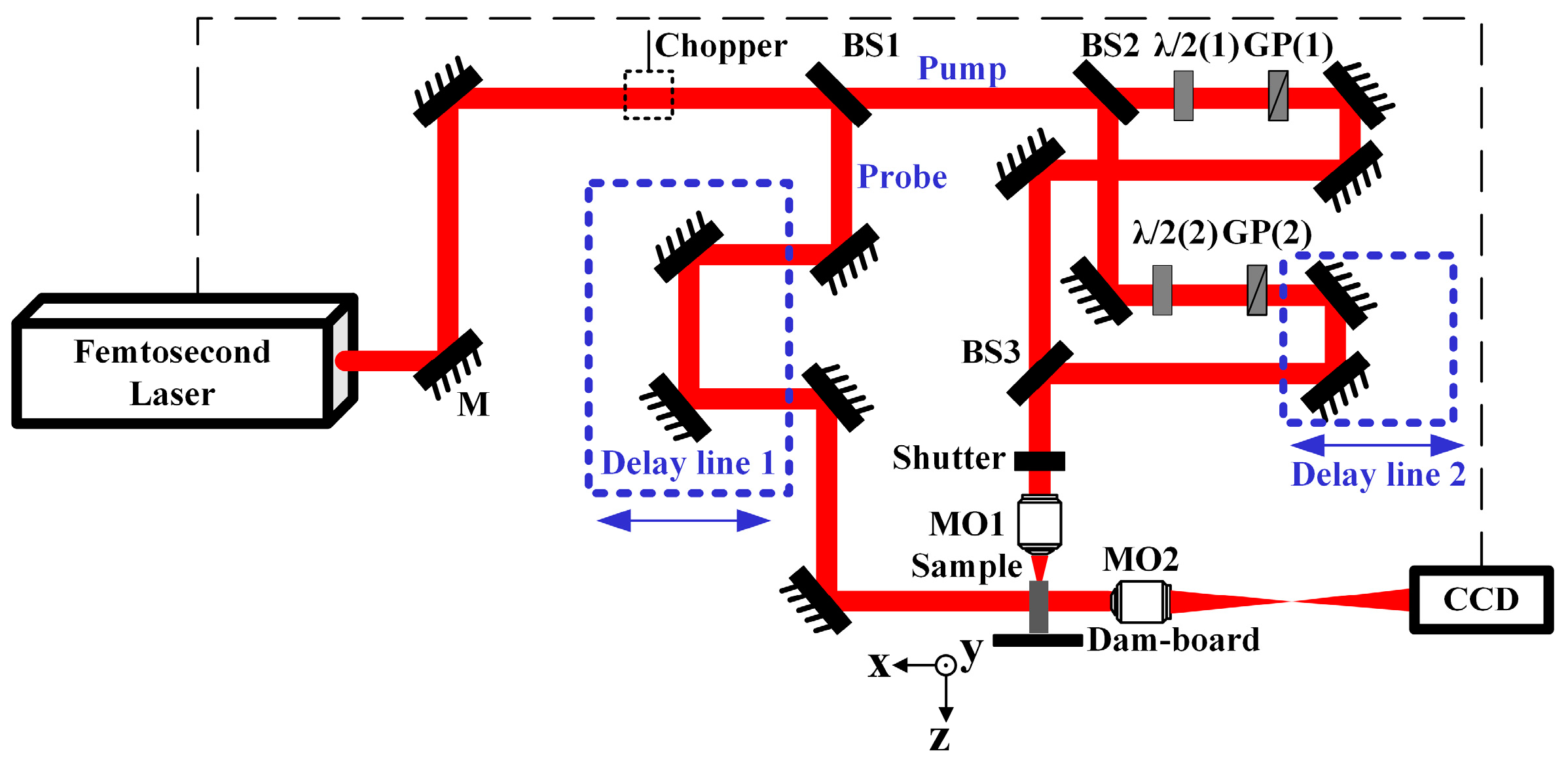
A schematic diagram of the experimental setup is shown in
Figure 1. An amplified Ti: sapphire laser (Astrella USP, Coherent, Santa Clara, CA, USA) generated a train of 1-kHz, 35 fs, and 800-nm horizontally polarized pulses with a Gaussian spatial profile. A pulse was split into pump and probe pulses using a beam splitter (BS
1). Both the pump and probe pulses have a wavelength of 800 nm. The pump pulse was guided into the Michelson interferometer to generate two subpulses, which were focused into the sample by the microscopic objective (MO
1 10×, NA = 0.3, Nikon Inc., Tokyo, Japan). Two pairs of λ/2 retarder plates and Glan prisms (GP) were used to adjust the energy of the two pump subpulses. The radius of the focal spot was ~1.27 μm. The t
s was controlled by changing the position of the mirror on a linear positioner mounted on the Michelson interferometer (delay line 2). The probe pulse passed through an optical delay line (delay line 1) to precisely control its delay times with respect to the pump pulses; it then illuminated the excitation region. Another microscope objective (MO
2 10×, NA = 0.3, Nikon Inc.) imaged the transmitted shadowgraph of the plasma on a monochrome charge-coupled device (CCD). The CCD was triggered by synchronized signals generated by the optical chopper, which was synchronized with the fs laser source. The duration of the probe pulse reaching the sample, as measured by a commercial autocorrelator (APE, Pulsecheck, Belin, Germany), was ~100 fs. Therefore, the temporal resolution of the experimental setup was considered to have reached ~100 fs. According to the Rayleigh criterion, the spatial resolution of the system is 1.62 μm. By incorporating a resolution chart (a chromium-coated glass U.S. Air Force resolution chart) in the probe light’s path, we achieved a system spatial resolution of ~2 μm. The time-resolved image recorded the variation in the intensity of the probe beam resulting from the fs laser-induced electron plasma and other phenomena. The sample used in the experiments was a 50 mm × 10 mm × 2 mm piece of fused silica with four polished surfaces. It was mounted on a computer-controlled three-dimensional stage and moved parallel to the y-direction at a speed sufficient to ensure no overlapping between each pulse-irradiated zone. The laser focusing depth in the sample was ~1 mm.
To initiate the experiment, we defined the first appearance time of weak electron plasma at the left edge of the image as the zero-delay time. In order to avoid confusion, the probe delay time was denoted by t to distinguish it from the pulses’ time separation (ts). In each experiment, the shadow image of the sample with and without pump light was recorded by the CCD camera. By calculating the ratio of the two images, the transmittance was obtained while the background noise was eliminated. The low transmittance area was where the strong absorption of the probe pulse by the pump pulse induced electron plasma.
3. Results and Discussion
In order to study the influence of the DP1 on the DP-induced electron plasma,
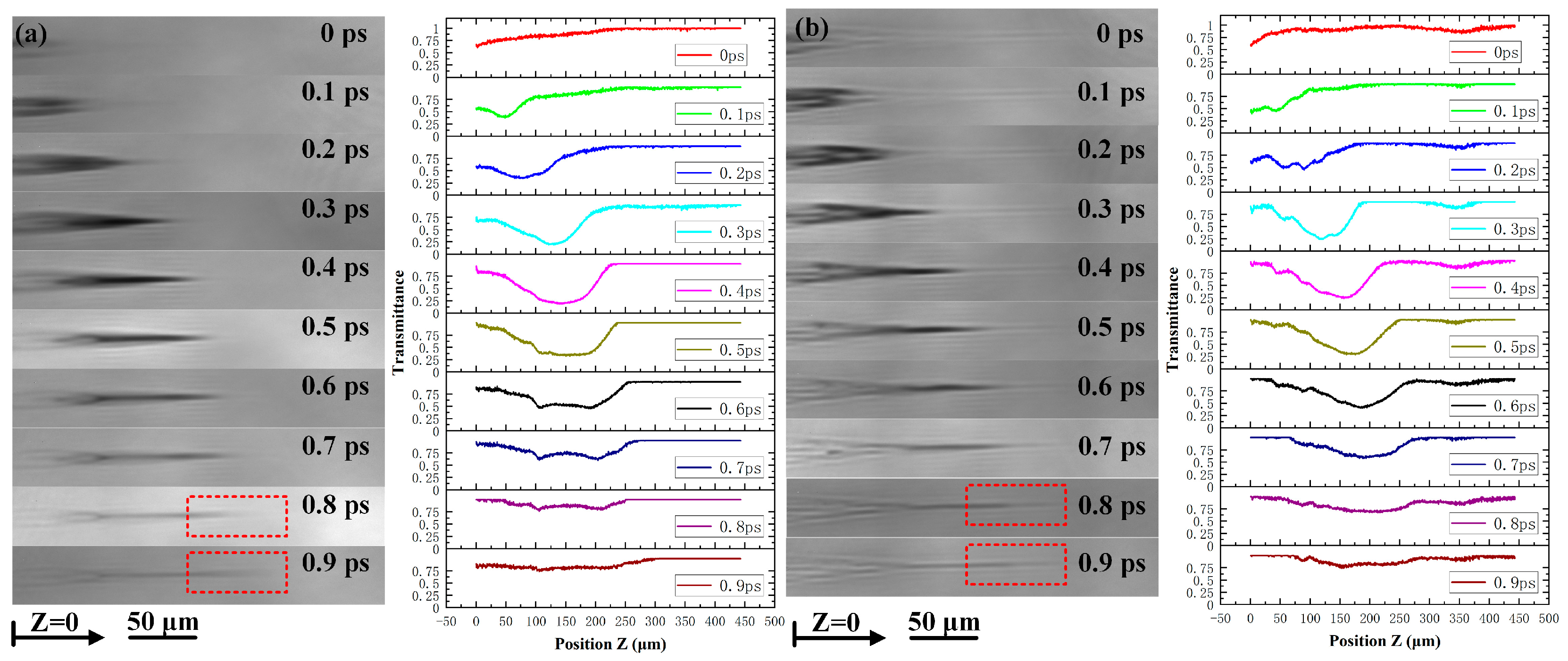
Figure 2 shows the two-dimensional transient transmission mapping and transmittance in the center of the electron plasma region after irradiation by the SP and DP2 (t
s = 2 ps) of DPs. The pulse energy for both the SP and DP2 was 4 μJ and the DP1 energy was 8 μJ.
Specifically,
Figure 2a shows two-dimensional transient transmission mapping and transmittance evolution at different delay times in the center of the electron plasma region after irradiation by the SP. At 0 fs, only weak filaments appeared in the image. As the delay time increased, the fs laser-induced filament gradually moved deeper into the sample due to the propagation of the laser pump pulse. In addition, a fork-like structure appeared near the incident surface, and then converged to a monofilament as the depth increased. Notably, it was found that the electron plasma region diffused after the filament length reached 60 μm at 0.8 and 0.9 ps, as shown in the red boxes in
Figure 2a. The fork structure near the laser pulse entrance may be due to the fork-like distribution of the pump light intensity caused by nonlinear optics and the spherical aberration effect of the interface [
19]. Due to the focusing effect, the fork structure converged to a monofilament and then slightly diffused in the deep part of the sample. As the laser focusing depth increases, the impact of spherical aberration becomes more pronounced [
19,
20]. This can cause the shape of the electron plasma region to change when processing is performed at different depths. Meanwhile, as the delay time increased, the minimum transmittance of the probe light increased first and then decreased. The minimum transmittance reached 0.184 at the position of 143.85 μm at 0.4 ps.
Figure 2b shows two-dimensional transient transmission mapping and transmittance evolution at different delay times in the center of the electron plasma region after irradiation by the DP2 (t
s = 2 ps) in fused silica. The transmittance evolution induced by the DP2 was actually formed by DPs. We defined the first appearance time of the DP2-induced electron plasma as a delay time of zero. At 0 fs, the free electrons induced by the DP1 have already relaxed [
17], and the 150 μm long filamentary shadow still existed in the map due to the self-trapped excitons induced by the DP1 in the fused silica, which has an ultra-long lifetime. The appearance of bright fused silica filaments may be caused by changes in the refractive index [
21]. Similarly to the process of the SP, the DP2-induced filament gradually moved into the deeper part of the sample, but the electron plasma induced by the DP2 did not diffuse at 60 μm in the filament region as the electron plasma region induced by the SP did at the same pulse energy; instead, it continued to move into the deeper part of the sample, as shown in the red boxes in
Figure 2b. The temporal and spatial evolution of the filament reflects the light propagation inside the material. Therefore, we believe that DP1-induced phase transitions, such as the refractive index change, acted as waveguides and confined the propagation of DP2 light inside the material. At 0.4 ps, the minimum transmittance reached 0.239 at the position of 152.95 μm. The lower transmittance means that the electron plasma absorbs the probe light more strongly. Therefore, the absorption of electron plasma induced by the SP was stronger than that induced by the DP2 at the same pulse energy.
The transient absorption coefficient of the electron plasma can be deduced from the obtained transmissivity. When the probe light passes through the electron plasma region, absorption, reflection, and refraction occur. Considering the cylindrical symmetry of the electron plasma region along the direction of the pump light transmission, the incident angle of the probe light passing through the axis of the electron plasma region is zero, and the refractive effect of the plasma on the probe beam can be ignored when studying the plasma distribution on the plasma axis. The reflection of the plasma on the probe beam is insignificant and can also be ignored [
22]. Only the absorption of the electron plasma on the probe beam is considered, and the intensity of the probe light, I
t, in the central region is [
23]:
The integral of Equation (1) can be described as:
where
is the length of the electron plasma region along the probe light propagation direction and
is the transient absorption coefficient. Furthermore, we can obtain the average absorption coefficient
aver as follows:
where
dia is the mean diameter of the electron plasma region in the
direction. By assuming the symmetric distribution of the electron plasma region in the
-
plane, we can deduce that
dia is equal to
dia, which is obtained from the transmissivity image. By assuming that the delay time of the minimum transmittance is the delay time of the strongest absorption of the electron plasma, we investigated the diameter of the electron plasma region of the minimum transmittance time delay image in the above experiments.
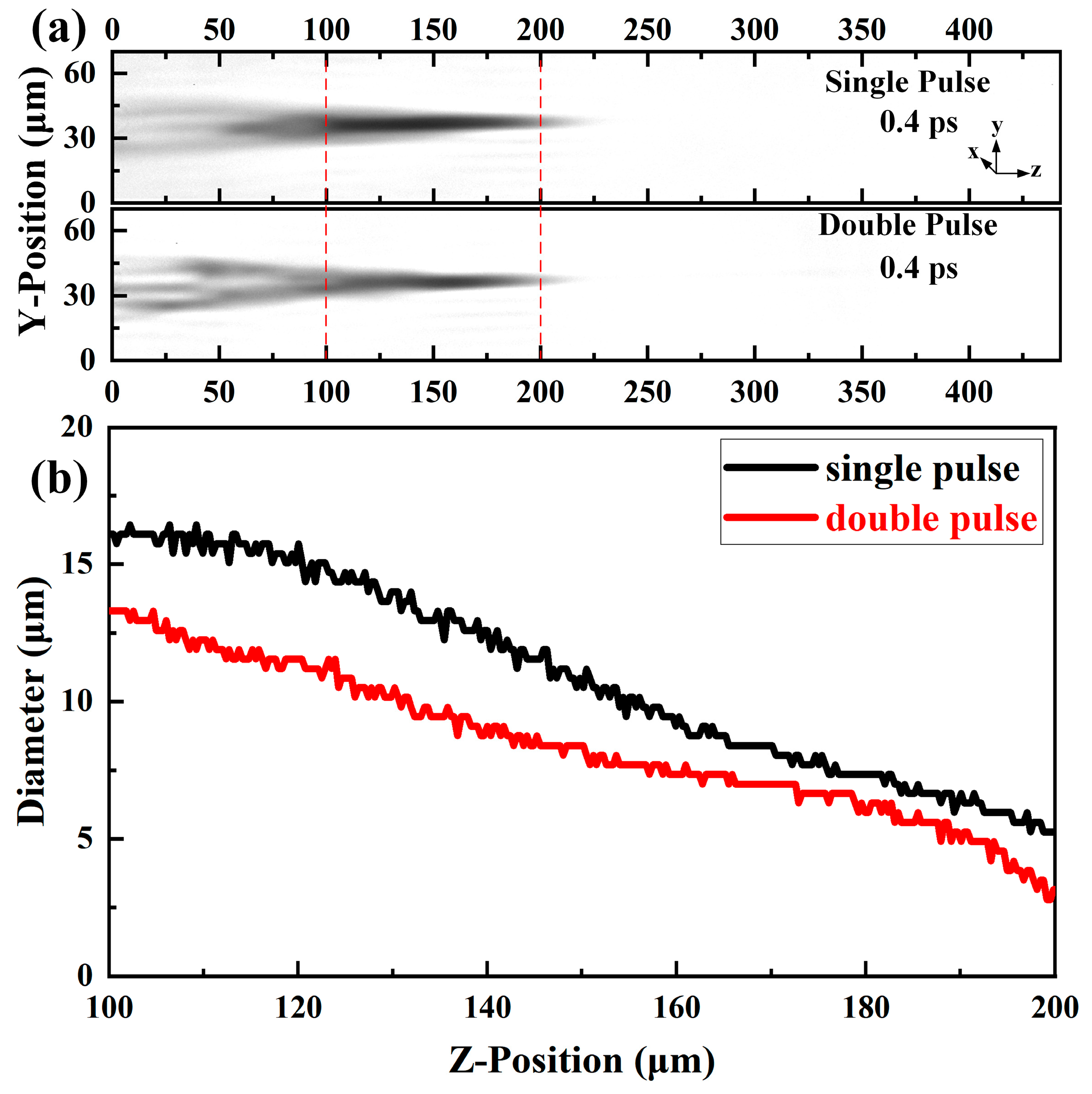
The transmittance in the above SP and DP experiments was at its minimum at a delay time of 0.4 ps.
Figure 3a shows the transmissivity distribution images at a delay time of 0.4 ps. The transmissivity distribution map allows the plasma regions with low transmissivity to be clearly distinguished for the analysis of the plasma region’s diameter. In order to prevent the plasma region with a fork-like structure near the laser incident surface from influencing the analysis of the plasma region diameter, the DP2-induced plasma region’s diameter is compared with a SP at the same pulse energy at the Z-position from 100 to 200 μm and the diameter is calculated from an absolute threshold. As shown in
Figure 3b, the plasma region diameters from 100 to 200 μm induced by a SP were larger than those induced by a DP2. Therefore, the electron plasma region induced by the DP2 was smaller than that induced by the SP at the same pulse energy, so the overall absorption of the electron plasma induced by the DP2 was weaker, which is why the minimum transmittance under the DP2 was larger than that under the SP at the same pulse energy, as shown in
Figure 2. Moreover, the electron density is proportional to the absorption coefficient of the probe light [
24]:
where n
e is the electron density, and
is the absorption cross-section for inverse bremsstrahlung according to the Drude method. This method is detailed in [
17]. We can obtain the transient electron density from the mean diameter of the electron plasma region and the transmittance. In order to simplify the calculation of the electron density, the mean diameter of the electron plasma region was calculated from the end of the plasma region with the fork-like structure to the deepest point; the values produced by the SP and DP2 were ~10.9 and 8.4 μm, respectively.
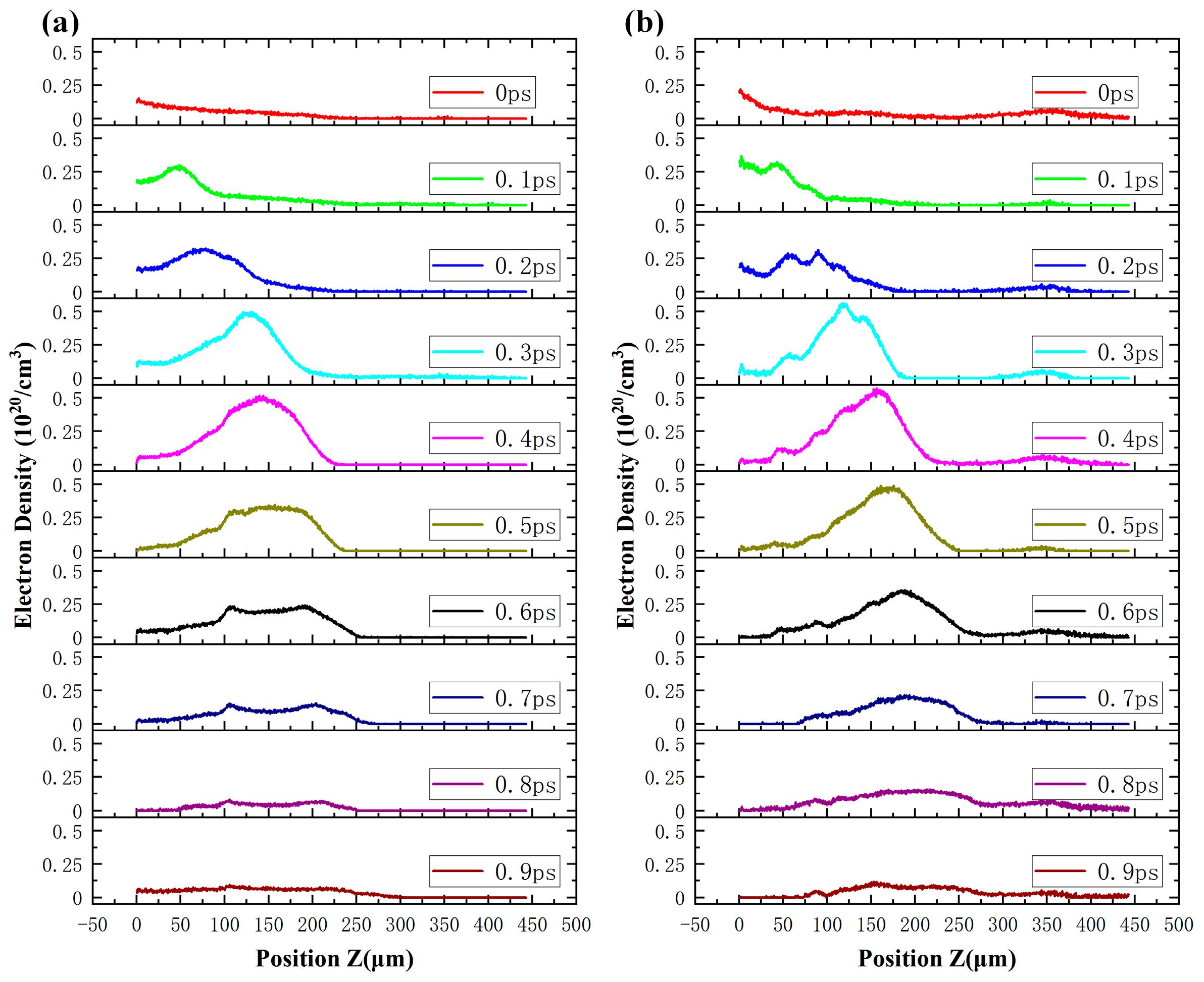
Figure 4 shows the spatial distribution of the transient electron density along the plasma region axis at different delay times for the SP and DP2. The transient peak electron densities and their corresponding spatial positions at different delay times were clearly observed. In the case of the SP, at 0.4 ps the maximum peak electron density reached 0.5171 × 10
20/cm
3 at the position of 143.85 μm. For the DPs, the maximum peak electron density induced by the DP2 reached 0.5676 × 10
20/cm
3 at the position of 152.95 μm at 0.4 ps. The maximum peak electron density induced by the DP2 was higher than that induced by the SP at the same pulse energy, which may be explained by the DP1-induced highly absorbing semi-metallic state of the warm dense glass in the fused silica [
9].
In addition, we studied the evolution of the DP-induced transient electron plasma with different DP1 energy values and compared these with a SP. The DP2-induced electron density reached its maximum at a delay time of ~0.4 ps under different DP1 energies.
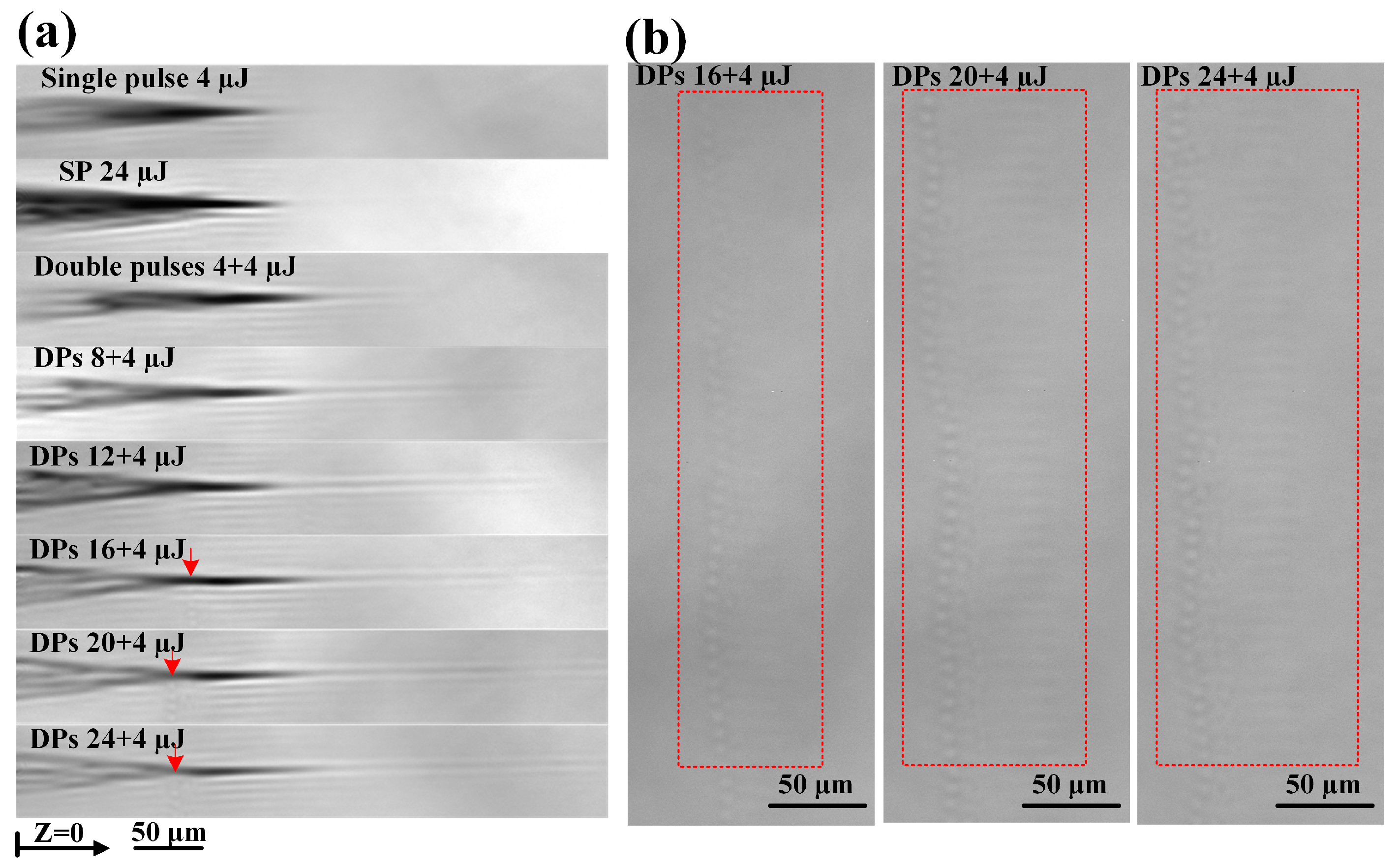
Figure 5a shows the time-resolved images of DP2 (t
s = 2 ps)-induced electron plasma at a delay time of 0.4 ps with different DP1 energy levels (4, 8, 12, 16, 20, and 24 μJ); the DP2 was fixed at 4 μJ and compared with a SP at different pulse energies (4, 24 μJ). Importantly, when the DP1 was increased to 16 μJ, the total energy of the DPs was 20 μJ; material damage can be observed in the fused silica, indicated by the red arrows in
Figure 5a. Notably, no damage was induced in the fused silica by the SP at 24 μJ. This implies that the damage produced in the DP experiment was induced by the DP2, and the DPs more easily induced damage in the fused silica compared with the SP process.
Figure 5b shows the structure generated by the DPs with different DP1 energies (16, 20 and 24 μJ). It can be seen that pronounced damage appeared inside the material, which was subsequently extended to the deeper part of the sample. The DP-induced damage also increased with the increase in the DP1 energy. The damage degree of the material is related to the pulse energy. Compared to single-pulse laser machining, dual-pulse machining exhibits a lower threshold energy for inducing damage in fused silica. As the laser energy surpasses the threshold, the damage degree of the material increases with the increase in energy [
17]. In addition, Chu et al. found that when using femtosecond laser DPs to fabricate microchannels in fused silica, the DP2 pulse with higher energy can more easily affect the medium within the t
s of 100 fs to 100 ps, resulting in the formation of a deeper microstructure [
25].
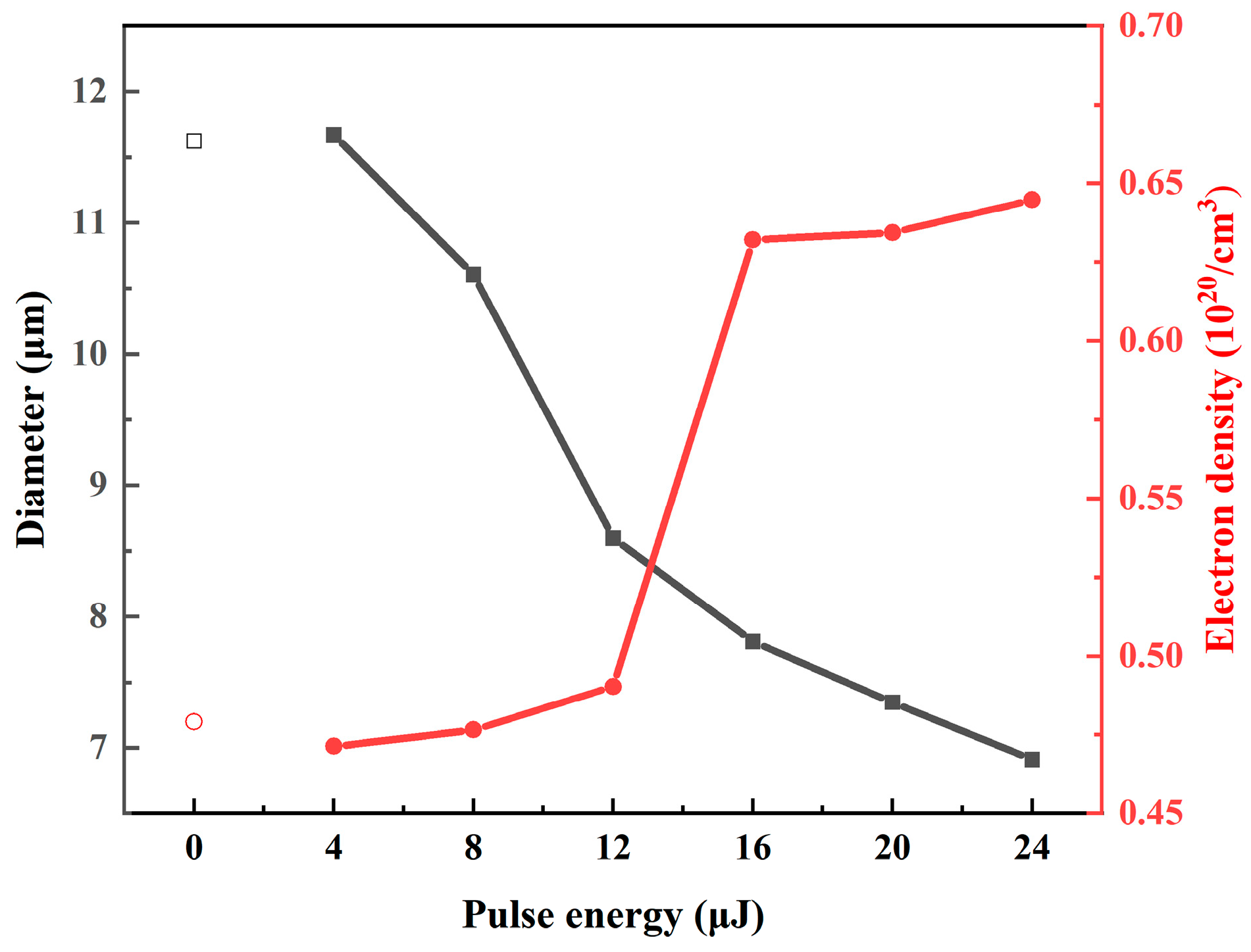
In addition, we studied the variation in the mean diameter of the electron plasma region and the maximum peak electron density induced by the DP2 with the energy of the DP1. The mean diameter of the electron plasma region was calculated from the end of the electron plasma region with the fork-like structure to the deepest part of the sample. As shown in
Figure 6, the hollow points represent the SP process as a reference, for a pulse energy of 4 μJ; the mean diameter of the SP-induced electron plasma region is ~11.6 μm. This is different from the above results, where the mean diameter of the electron plasma region was 10.9 μm at the same energy value. This is because the two groups of experiments were carried out on different samples and there was a deviation in the laser focusing depth, which affected the results. As the DP1 energy increased from 4 to 24 μJ, the mean diameter of the DP2-induced electron plasma region decreased from 11.6 μm to 6.9 μm. The maximum peak electron density induced by the SP was ~0.479 × 10
20/cm
3. The DP2-induced electron density was increased from 0.471 × 10
20/cm
3 to 0.644 × 10
20/cm
3. The damage threshold electron density of the fused silica induced by the DP2 was defined as the maximum peak electron density at 16 μJ of the DP1 energy and was 0.63 × 10
20/cm
3, which was less than the damage threshold electron density induced by the SP [
17]. In short, as the DP1 energy increased, the diameter of the DP2-induced electron plasma region further decreased, and the maximum peak electron density increased. This may be because the higher the DP1 energy, the stronger the induced high-absorption semi-metallic phase transition compared to the surrounding area. Therefore, the DP2-induced electron plasma region is more concentrated in the strong phase transformation region and the maximum peak electron density increases. The reduction in the diameter of the electron plasma region may also be due to the stronger waveguide-like effect.
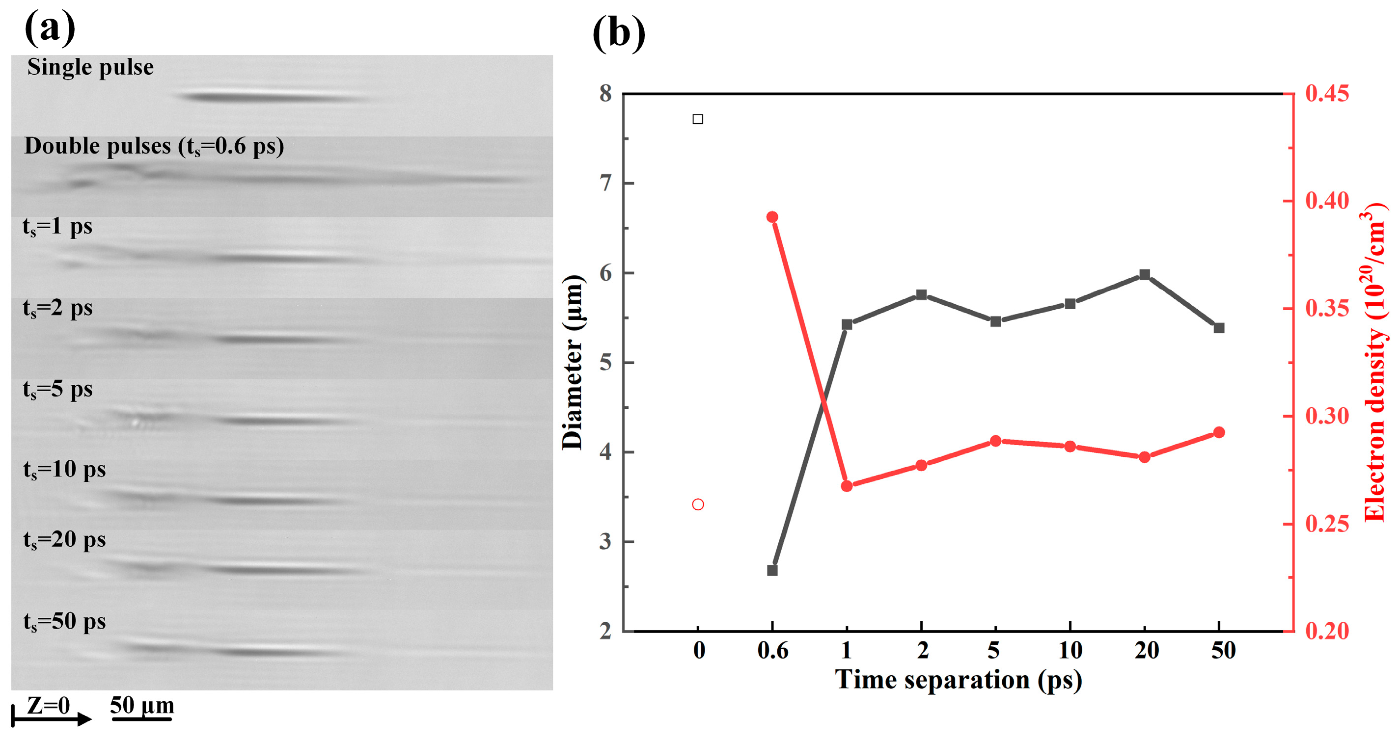
Moreover, we studied the evolution of the transient electron plasma induced by a DP2 at different t
s values and compared it with a SP. The DP2-induced electron density reached its maximum at a delay time of ~0.4 ps at different t
s values;
Figure 7a shows the time-resolved images of the DP2-induced electron plasma with different t
s values (0.6, 1, 2, 5, 10, 20, and 50 ps) at a delay time of 0.4 ps compared with a SP. The SP and DP2 energy levels were both 2 μJ and the DP1 energy was 4 μJ. As shown in
Figure 7a, when the t
s value was 0.6 ps, the free electron density induced by the DP1 was still high, and the highly reflective surface formed by the free electrons meant that the electron plasma induced by the DP2 could be divided into two weak filaments, which is consistent with the phenomenon described in [
18]. When t
s increased, this splitting phenomenon did not occur because the electron density relaxed to a lower value. As shown in
Figure 7b, the hollow points represent the SP process as a reference; for a pulse energy of 2 μJ, the mean diameter of the SP-induced electron plasma region was ~7.7 μm. When the t
s was 0.6 ps, the mean diameter of the electron plasma region was only 2.6 μm due to the splitting phenomenon. The mean diameter of the DP2-induced electron plasma region remained at ~5.5 μm when the t
s increased from 1 ps to 50 ps. The maximum peak electron density induced by the SP was 0.25 × 10
20/cm
3. When the t
s was 0.6 ps, the maximum peak electron density induced by the DP2 was 0.39 × 10
20/cm
3. The maximum peak electron density induced by the DP2 essentially remained around ~0.3 × 10
20/cm
3 when the t
s increased from 1 ps to 50 ps. In summary, the mean diameter of the electron plasma region and the maximum peak electron density induced by the DP2 remained almost unchanged when the ts was changed from 1 to 50 ps; this is mainly due to the long relaxation time of the phase transition caused by the DP1.


