Communication

Subwavelength-Scale 3D Broadband Unidirectional Waveguides Based on Surface Magnetoplasmons at Terahertz Frequencies

Department of Applied Physics, Zhejiang University of Technology, Hangzhou 310023, China
*
Author to whom correspondence should be addressed.
Photonics 2023, 10(5), 589; https://doi.org/10.3390/photonics10050589
Submission received: 7 April 2023 / Revised: 16 May 2023 / Accepted: 16 May 2023 / Published: 18 May 2023
(This article belongs to the Special Issue New Trend in Nanophotonics)

Abstract

:
Unidirectional electromagnetic modes have significant potential for routing electromagnetic radiation and are highly desirable for various applications, such as isolators, splitters, and switches. In this study, we theoretically investigate surface magnetoplasmons (SMPs) in a four-layer structure consisting of a perfect magnetic conductor (PMC)–semiconductor–dielectric–metal, which exhibits complete unidirectional propagation. We extend this structure to a 3D model by decreasing the width of the PMC-semiconductor part to an appropriate value and demonstrate that the SMPs in the proposed 3D waveguide retain complete unidirectional propagation. Our findings indicate that the unidirectional SMPs are robust to backscattering caused by surface roughness and defects. Moreover, the proposed 3D waveguide can be efficiently coupled to conventional microstrip line waveguides. Our results (based on the numerical method) demonstrate that SMPs based on semiconductors offer a promising approach to creating devices with new functionalities in the terahertz regime below the diffraction limit.

1. Introduction

Unidirectional electromagnetic (EM) modes, first proposed by Haldane [1] as analogs of quantum Hall edge states, and experimentally demonstrated in microwave regimes using magneto-optical (MO) materials [2], have received significant attention in research due to their widespread applications in optical communication [3,4]. These modes can be realized in MO heterostructures [5,6,7], which are technically the simplest way to build one-way waveguides, or in topologically protected systems [3,8,9,10]. In MO heterostructures, unidirectional EM modes are typically transmitted in the form of surface magnetoplasmons (SMPs) [11,12]. SMPs are collective oscillations of charge carriers in MO materials under static external magnetic fields, and they exhibit nonreciprocity due to the breaking of time-reversal symmetry by the external magnetic field [5,13,14,15]. One of the most striking findings in the study of unidirectional SMPs is that the time-bandwidth limit in physics and engineering can be overcome by exploiting unidirectional SMPs in MO heterostructures systems due to the broken Lorentz reciprocity [6]. Other potential applications based on unidirectional SMPs in MO heterostructures, such as true rainbow trapping [16], beam splitters [17,18], isolators [19], and large-area unidirectional EM modes [20], have been demonstrated.
The study of unidirectional SMP waveguides has mainly focused on 2D configurations due to the inherently two-dimensional nature of SMPs, where electromagnetic fields degrade exponentially with distance from the surface [21]. Unidirectional SMPs are typically achieved using two types of MO materials: doped semiconductors in the terahertz regime and ferrites in the microwave regime. In the microwave regime, SMPs exhibit transverse-electric (TE) polarization due to the gyromagnetic effect of the ferrite under a moderate external magnetic field. Consequently, SMPs based on ferrites can be straightforwardly extended to 3D configurations by truncating metal slabs in the lateral directions [22]. In contrast, SMPs based on doped semiconductors in the terahertz regime exhibit transverse-magnetic (TM) polarization due to the gyroelectric effect. As a result, extending SMPs in semiconductors to a more realistic 3D case using the same strategy as in the microwave regime is not feasible. Doped semiconductors under external magnetic fields exhibit two band gaps: the intrinsic band gap and an additional high-frequency band gap opened only in the presence of a magnetic field. Previous research on unidirectional SMPs has mostly focused on these types of SMPs located in the low-frequency band gap (the intrinsic band gap) of the semiconductors, which exhibit a unidirectional propagation interval between the two asymptotic frequencies of forward and backward-propagations [5,6]. However, these SMP types no longer have asymptotic frequencies (i.e., the frequency of SMPs increases continuously as the wave vector increases) when non-local effects are considered, which makes the unidirectional interval that is dependent on the differences between asymptotic frequencies lose its physical validity [23]. In contrast, SMPs within the high-frequency band gap of the semiconductor in opaque material–semiconductor structures can still exhibit unidirectional propagation even when non-local effects are considered, as demonstrated by Monticone et al. [24]. Although these SMPs are leaky modes and suffer from severe material loss due to the dispersive nature of the opaque material and semiconductor, they still serve as effective alternatives for realizing unidirectional SMP modes in MO heterostructures. Therefore, achieving 3D unidirectional terahertz SMP waveguides using MO heterostructures is currently an ongoing progress.
In this paper, we propose a 3D waveguide that supports unidirectional propagating SMPs in the terahertz regime. The waveguide is composed of a perfect magnetic conductor (PMC)–semiconductor–dielectric–metal-layered structure, with a semiconductor layer of finite width on a grounded dielectric substrate. The complete one-way propagation (COWP) band of the SMP is located in the high-frequency band gap of the semiconductor. To analyze the dispersion properties and mode profiles of the SMP, we theoretically investigated a 2D PMC–semiconductor–dielectric–metal-layered structure and extended our analysis to a 3D scenario using finite element methods. Our numerical analysis shows that the SMPs propagate unidirectionally without backscattering, even in the presence of obstacles or fabrication defects. We also demonstrate that the 3D waveguide can be effectively coupled with conventional microstrip line waveguides and present a 3D isolator with a subwavelength scale at terahertz frequencies using the proposed waveguide.

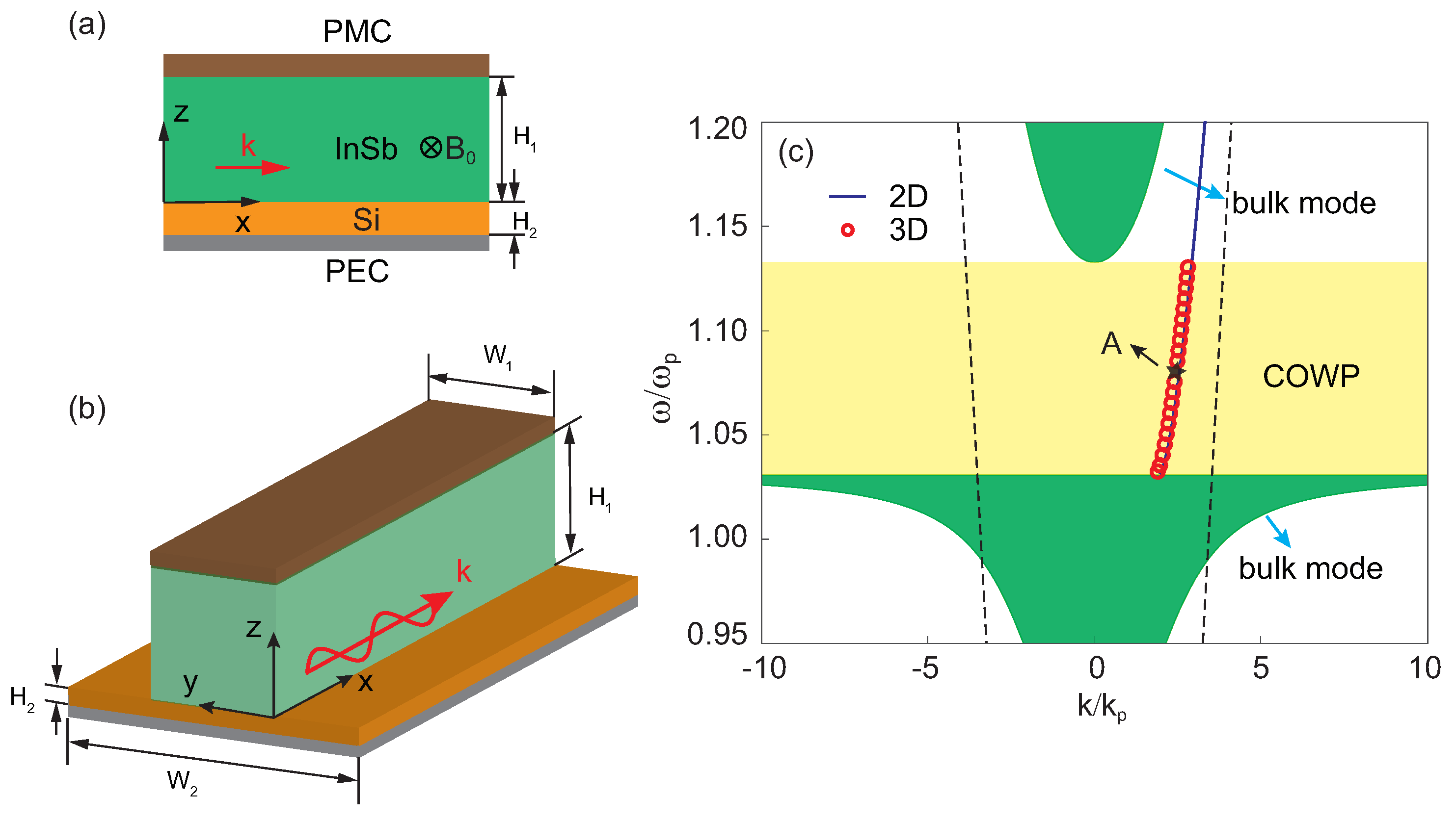
2. Basic Physical Model
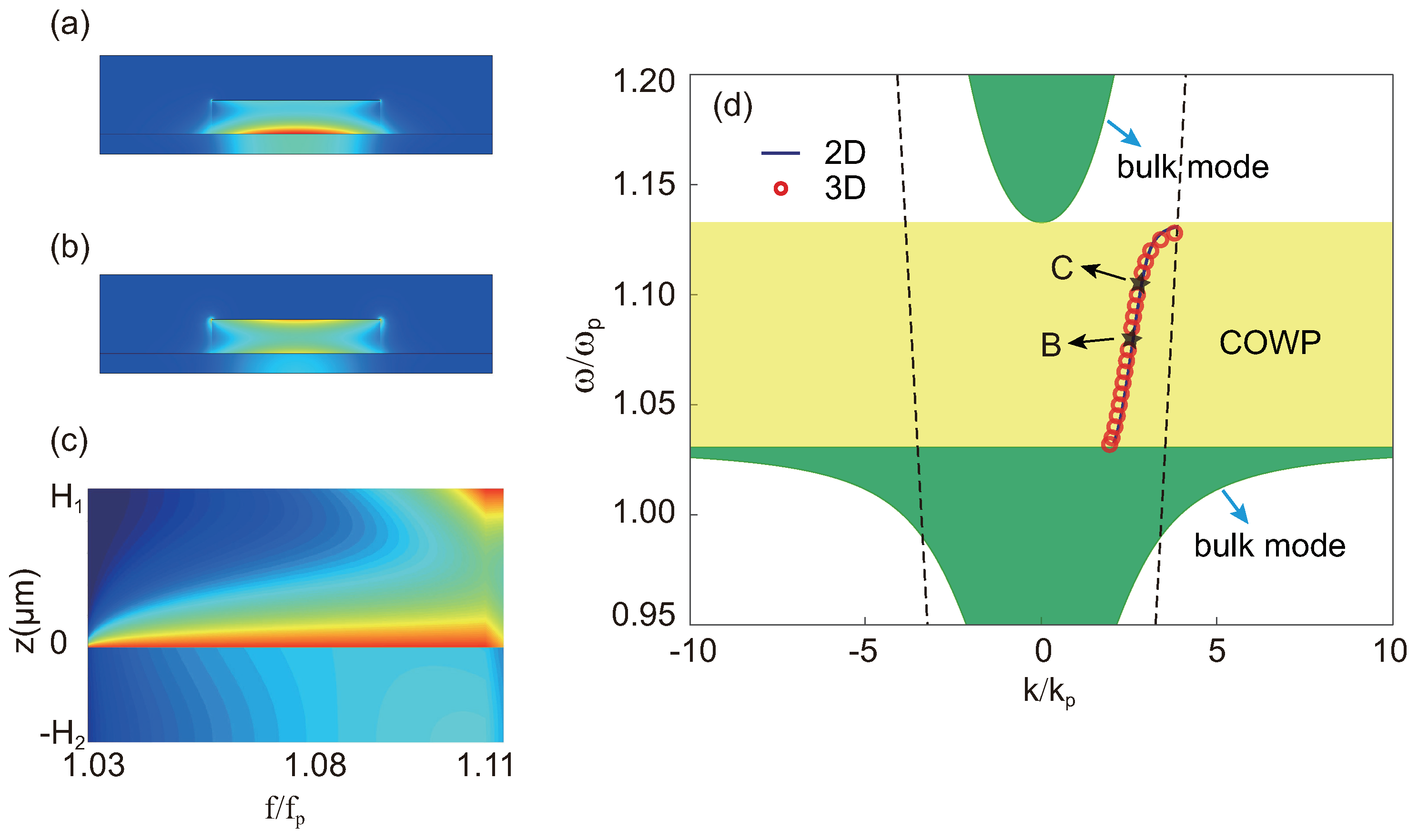
The physical model for 2D one-way SMPs operating at terahertz frequencies is depicted in Figure 1a. The waveguide system comprises a layered structure consisting of a PMC–semiconductor–dielectric–metal. The metal layer is assumed to be a perfect electric conductor (PEC), which is a good approximation in the terahertz regime. The dielectric layer has a thickness of H 2 with relative permittivity ϵ r , and the semiconductor layer has a thickness of H 1 . The semiconductor layer is uniformly magnetized by an external DC magnetic field B 0 in the y direction, and SMPs propagate along the x direction. Gyroelectric anisotropy is induced in the semiconductor by the external magnetic field, with the permittivity tensor taking the following form:
ϵ s = ϵ 1 0 i ϵ 2 0 ϵ 3 0 i ϵ 2 0 ϵ 1
with
ϵ 1 = ϵ ( 1 ω p 2 ω 2 ω c 2 ) ,
ϵ 2 = ϵ ω c ω p 2 ω ( ω 2 ω c 2 ) ,
ϵ 3 = ϵ ( 1 ω p 2 ω 2 ) ,
where ω is the angular frequency, ω p is the plasma frequency of the semiconductor, ω c = e B 0 m * (where e and m * are, respectively, the charge and effective mass of the electron) is the electron cyclotron frequency, and ϵ is the high-frequency (relative) permittivity of the semiconductor. Here, it is presumed that the semiconductor is lossless, and material loss will be taken into account in the transmission simulation. We first investigate the dispersion of SMPs in this 2D system. The EM fields of SMPs are TM-polarized, and the nonzero component of the magnetic field can be written as
H y ( x , z ) = [ A 1 e x p ( i p z ) + A 2 e x p ( i p z ) ] e x p [ i ( k x ω t ) ] ,
in the dielectric layer for H 2 < z 0 and
H y ( x , z ) = [ B 1 e x p ( α z ) + B 2 e x p ( α z ) ] e x p [ i ( k x ω t ) ] ,
in the semiconductor for 0 < z H 1 , where k is the propagation constant, p = ϵ r k 0 2 k 2 (where k 0 is the wavenumber in vacuum), and α = k 2 ϵ v 2 k 0 2 with ϵ v = ϵ 1 ϵ 2 2 ϵ 1 being the Voigt permittivity [25]. The nonzero components of the electric field ( E x and E z ) can be obtained straightforwardly from H y . The tangential component E z must vanish at the metal boundary at z = H 2 , and the H y must vanish at the PMC boundary at z = H 1 . The boundary conditions further require that the field components E x and H y be continuous at the semiconductor–dielectric interface. Based on this, the dispersion relation for the proposed structure is determined and it has the form
α tanh ( α H 1 ) + ϵ 2 ϵ 1 k ϵ v ϵ r p tan ( p H 2 ) = 0 .
When the thickness of the semiconductor tends to be infinite, i.e., H 1 , Equation (7) is simplified to the following form
α + ϵ 2 ϵ 1 k ϵ v ϵ r p tan ( p H 2 ) = 0 .
In this context, the thickness of the semiconductor is specified as H 1 = 0.5 λ p (where λ p is the vacuum wavelength for the plasma frequency). It is noted that the dispersion relations obtained using Equations (7) and (8) almost coincide within the frequency range shown in Figure 1c. The semiconductor is assumed to be InSb with ϵ = 15.6 , ω p = 4 π × 10 12 rad/s and ω c = 0.25 ω p (corresponding to B 0 = 0.27 T ). The dielectric layer used in the structure is silicon with ϵ r = 11.68 , and its thickness is set to H 2 = 0.06 λ p . Note that our analysis focuses on the high-frequency band gap of the semiconductor, where SMPs of this type exhibit unidirectional propagation properties even when non-local effects are present [24]. On the other hand, although the dispersion curves obtained from Equation (7) have solutions in the low-frequency band gap of the semiconductor (ranging from 0 to 0.88 ω p , not shown in Figure 1c), these SMPs do not possess unidirectional propagation properties in this region when non-local effects are considered [23], which is not of interest to us. This design guarantees the absence of regular bidirectional modes guided by zigzag reflections between the metal and semiconductor surfaces, as the dielectric thickness is kept below the critical value necessary for the appearance of such modes [26]. It is worth mentioning that a PMC is used to truncate the semiconductor in order to preserve the single-mode unidirectional nature of the 3D waveguide. This is because PEC–semiconductor interfaces usually support unidirectional SMPs that can potentially interfere with the SMPs at the semiconductor–dielectric interface. Figure 1c clearly shows that there exists only one SMP mode with a positive group velocity in the COWP region. This implies that SMPs in this region are immune to backscattering even in the presence of fabrication imperfections or defects, as there is no backpropagating mode.
The feasibility of extending the proposed 2D one-way waveguide to a practical 3D system is of interest. As shown in Figure 1b, the PMC and semiconductor components are bounded by air of finite width W 1 in the y direction. Obtaining fully analytical solutions for this 3D system is not a straightforward task and, thus, we employed numerical methods to investigate the dispersion relations of SMPs within the proposed waveguide. The results, presented in Figure 1c and obtained through the finite element method, demonstrate good agreement between the dispersion of the fundamental mode in the 3D system and that in the aforementioned 2D system. Therefore, the proposed 3D waveguide also exhibits robust unidirectional propagation properties for SMPs, with only a slightly smaller wave vector compared to the 2D case.

3. Modal Properties

Using the finite element method, we investigate the mode profiles and transmission characteristics of the 3D waveguide system, with parameters identical to those shown in Figure 1. In the simulation, the SMPs are excited by a magnetic current line positioned 1 μ m below the semiconductor–dielectric interface. The operation frequency f o = 1.08 f p (where f p = ω p / 2 π ) is at the center of the COWP range, as marked by point A in Figure 1c. It is obvious from Figure 2a that SMPs operating within the COWP range can only propagate along the + x direction in the proposed 3D waveguide. To further examine the robustness of the unidirectional propagating property, we introduced a metal cuboid as an obstacle along the propagating path of the SMPs, as depicted in Figure 2b. The dimensions of the obstacle are 8 μ m in length, 50 μ m in width, and 10 μ m in height. To better visualize the internal electric field distribution, the side surface (indicated by the white dashed line) is omitted in Figure 2a,b. Obviously, SMPs are capable of bypassing the metal cuboid and propagating unidirectionally without any backscattering. Furthermore, the cutting slices in Figure 2d,e indicate that the metal cuboid obstacle can only distort the field distribution of SMPs within a limited range of distances. The field distribution of SMPs behind the obstacle quickly recovers and is basically the same as that without the obstacle.
In the proposed 3D unidirectional waveguide, the mode profile of SMPs is significantly affected by the thickness of the semiconductor. When the thickness of the semiconductor layer is large (for example, H 1 = 0.5 λ p , as described in the previous sections), the electric fields of SMPs are concentrated at the semiconductor–dielectric interface throughout the entire COWP range, as illustrated in Figure 2c. Comparing Figure 1c and Figure 3d, it is evident that the dispersion curve of SMPs significantly deviates in the higher portion of the COWP range as the thickness of the semiconductor decreases. The dispersion relations and mode profiles of SMPs are illustrated in Figure 3 for a semiconductor layer thickness of 0.1 λ p , with all other parameters being identical to those in Figure 2. As shown in Figure 3c, when the operating frequency increases, the electric fields of SMPs become more diffuse and occur at the PMC-semiconductor interface as well as the semiconductor–dielectric interface. SMP modes with a more concentrated field distribution are more compatible with conventional waveguides. Therefore, the thickness of the semiconductor layer is supposed to be 0.5 λ p .

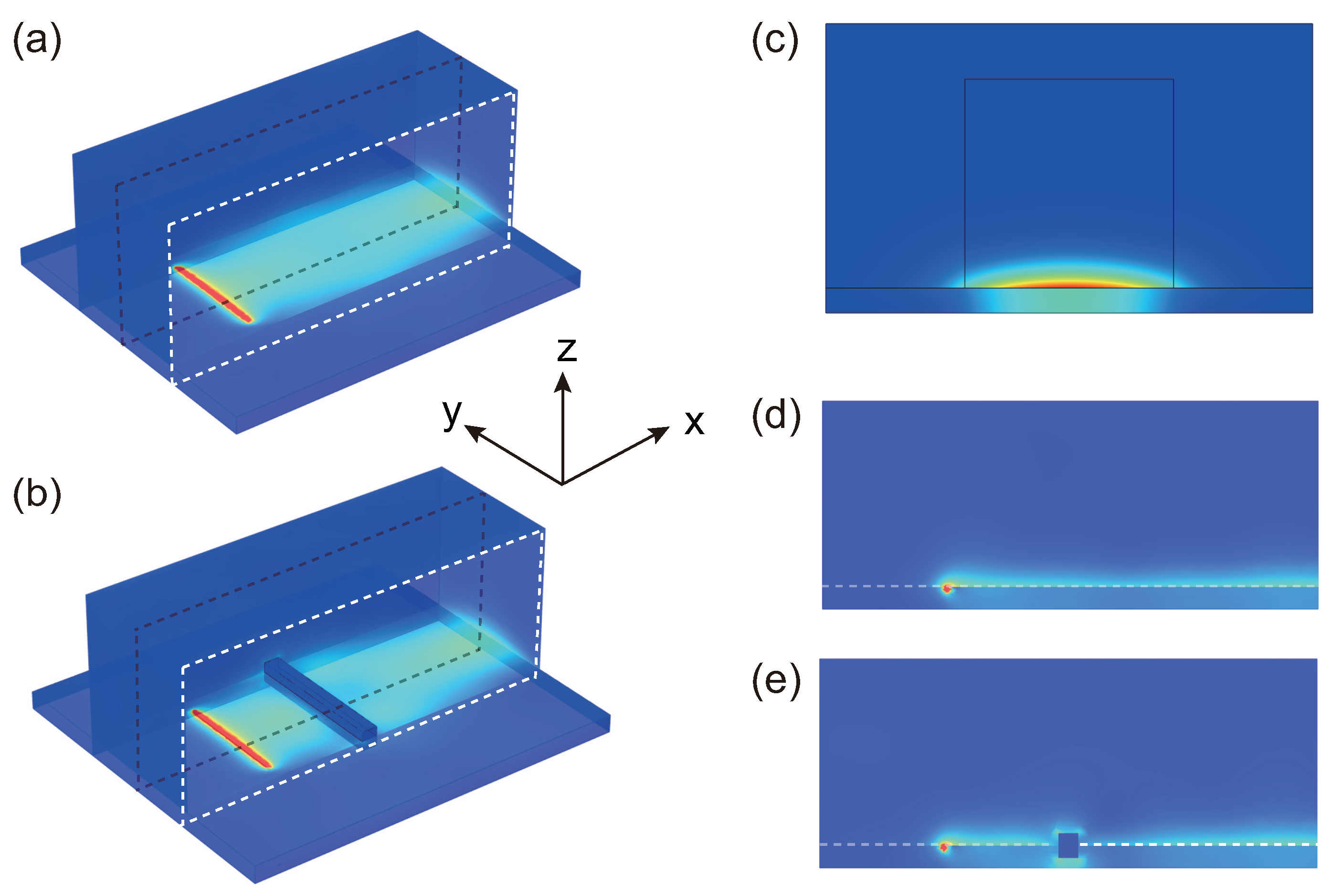
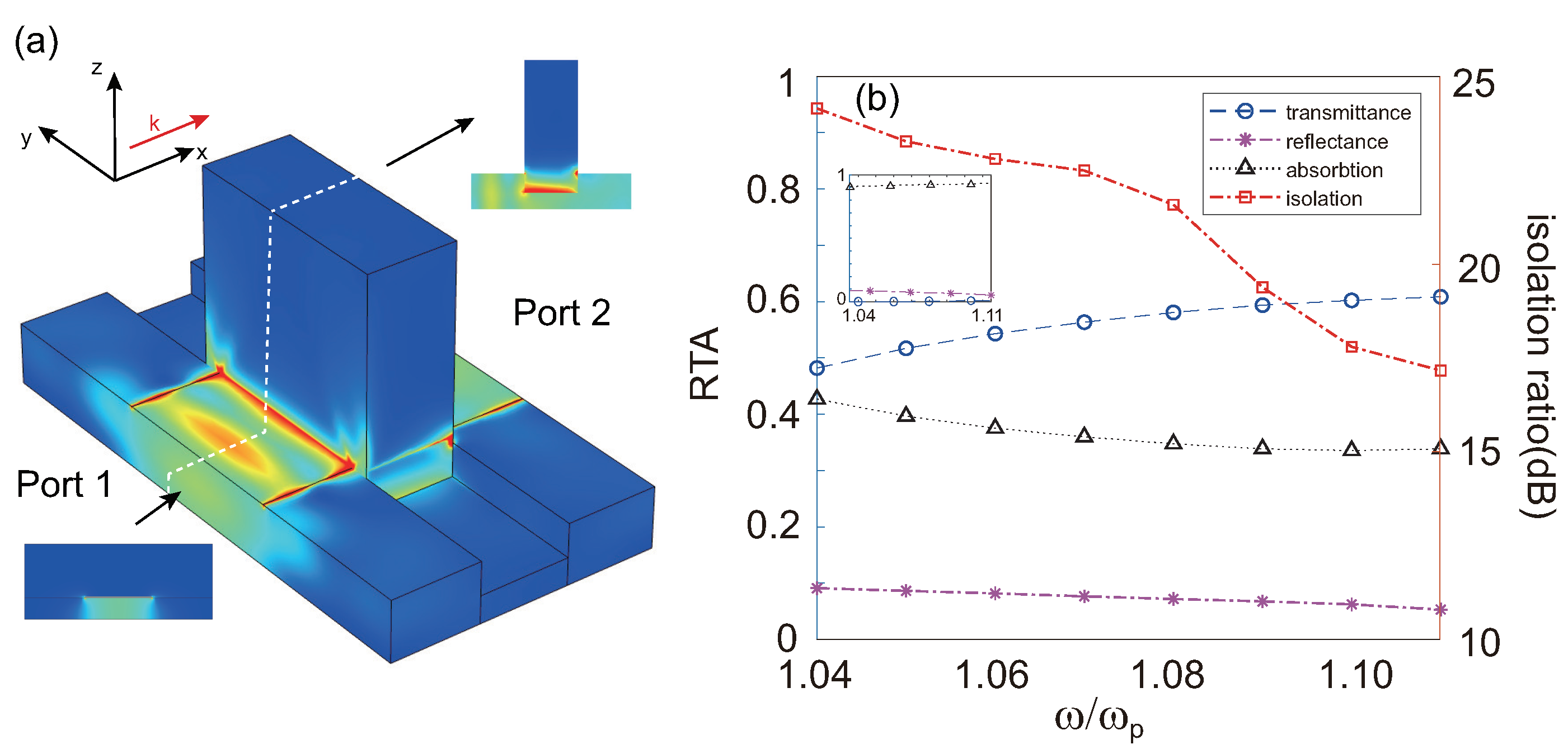
4. Subwavelength Isolator

After clarifying the dispersion characteristics and mode profiles of SMPs in the proposed 3D one-way waveguide, we now consider its application in an optical system as an isolator. Connecting a plasmonic waveguide to a conventional optical waveguide is challenging due to the different modal field profiles in the two systems. However, the electric field distribution of SMPs in the proposed one-way waveguide is similar to that of the quasi-transverse electromagnetic (TEM) mode in a traditional microstrip line waveguide. As a result, it is possible to achieve efficient coupling between these two systems with proper design.
We first conducted a numerical simulation on a metal slab waveguide that is linked to the proposed one-way waveguide in a 2D scenario. To match the modal sizes in the two systems, the metal slab waveguide is filled with silicone with ϵ r = 11.68 . As an optical device, the absorption of the semiconductor is taken into account, resulting in Equations (2) and (3) becoming
ϵ 1 = ϵ 1 ( ω + i v ) ω p 2 ω [ ( ω + i v ) 2 ω c 2 ] ,
ϵ 2 = ϵ ω c ω p 2 ω [ ( ω + i v ) 2 ω c 2 ) ] ,
where v is the electron scattering frequency. The length of the one-way waveguide is L 0 = 0.2 λ p and the electron scattering frequency is v = 0.05 ω p . The distance between the two metal slabs is set to 20 μ m , ensuring that there is no third-order TM mode within the COWP region and that the transmittance remains relatively high. We subsequently expanded the 2D metal slab waveguide into a 3D microstrip line waveguide, with the structure and mode profiles depicted in Figure 4a. By comparing the mode profiles shown in the inserts of Figure 2c and Figure 4a, we can observe that the electric field of the microstrip line waveguide is concentrated between the two metal slabs, which is similar to the field distribution in the substrate layer of the proposed 3D one-way waveguide.
Based on the analyses above, we proposed an isolator consisting of the suggested unidirectional waveguide and two conventional microstrip line waveguides, as shown in Figure 4a. The amplitudes of the electric field for a forward-propagating wave (along the + x direction) at the center of the COWP range with an operating frequency f o = 1.08 f p are illustrated. In the simulation, the metal is assumed to be PEC, which is a good approximation in the terahertz regime. For a forward-propagating wave (along the + x direction) in the COWP region, the fundamental mode of the conventional microstrip line waveguide is excited by Port 1, which then converts to the plasmonic mode in the proposed 3D unidirectional waveguide. Afterward, the plasmonic mode propagates unidirectionally through the center part, converting back to the fundamental mode without any backscattering, and ultimately exports through Port 2. On the contrary, when excited from Port 2 in the reverse direction (along the x direction), the proposed 3D unidirectional waveguide blocks the electromagnetic wave, as no mode propagating in the negative ( x ) direction is supported. The inset at the upper right corner of Figure 4a shows the electric field distribution of the cutting slice, which is indicated by a white dashed line and located at the center of the isolator. Figure 4b shows the numerical results for wave transmittance, reflectance, absorption, and isolation ratio spectra within the COWP region for forward-propagating waves, while the inset shows the spectra for backward-propagating waves. Reflectance is almost identical for both propagating directions, while absorption exceeds 90% for backward-propagating waves. Within the COWP region, the transmission for the forward-propagating wave is approximately 50% to 60%, while that for the backward-propagating waves is below 1%, resulting in an isolation ratio above 17 dB for a 3D unidirectional waveguide length of only 0.2 λ p . The proposed structure enables a wider bandwidth for the isolator than that of typical isolators due to the width of the COWP region. In particular, the proposed isolator has a bandwidth of 0.14 THz, which is significantly greater than the typical range of 0.14–50 GHz for other terahertz isolators [27,28,29]. The isolation ratio (in dB) is almost linearly related to the length of this kind of unidirectional waveguide [22], as the field strength of the backward-propagating wave decays exponentially along the backward direction. This linear relationship allows for the straightforward achievement of higher isolation ratios by increasing the waveguide length.
Our theoretical model for unidirectional waveguides based on SMPs in semiconductors can serve as a guide for future experiments. However, conducting experiments is currently challenging because the necessary equipment is unavailable; our terahertz platform is still under construction.

5. Conclusions

In this study, we theoretically demonstrated that the broadband unidirectional propagation of SMPs can be realized in a 3D structure consisting of a PMC–semiconductor–dielectric–metal at terahertz frequencies. The dispersion relations for SMPs in the proposed waveguide were systematically investigated, and the effects of the semiconductor thickness on the dispersion were also carefully addressed. Our results based on analytical and numerical methods reveal that the proposed 3D waveguide can provide a robust unidirectional propagating region for SMPs. The COWP region of the SMPs is located in the high-frequency band gap of the semiconductor, indicating that these SMPs can still exhibit unidirectional properties even when non-local effects are considered. Additionally, due to the similar modal profiles of the SMP mode in the 3D waveguide and the quasi-TEM mode in a traditional microstrip line waveguide, efficient coupling between these two systems can be achieved with proper design. Based on the unidirectional waveguide, we have proposed a high-quality broadband isolator at a subwavelength scale in the terahertz regime. The proposed 3D unidirectional waveguide has promising applications for novel compact optical components at terahertz regimes, such as broadband splitters, circulators, sensors, and field-enhancement devices [30,31,32].

Author Contributions

Conceptualization, Y.Y. and L.S.; methodology, Y.Y., H.B. and Q.S.; simulation, H.B., Y.Y. and Q.S. All authors have read and agreed to the published version of the manuscript.

Funding

This research was funded by the National Natural Science Foundation of China, grant numbers 62101496 and 62075197, and the Science Foundation of Zhejiang Province, grant number LQ21F010013.

Institutional Review Board Statement

Not applicable.

Informed Consent Statement

Not applicable.

Data Availability Statement

The data that support the findings of this study are available from the corresponding author upon reasonable request.

Conflicts of Interest

The authors declare no conflict of interest.

References

  1. Raghu, S.; Haldane, F.D.M. Analogs of quantum-Hall-effect edge states in photonic crystals. Phys. Rev. A 2008, 78, 033834. [Google Scholar] [CrossRef]
  2. Wang, Z.; Chong, Y.; Joannopoulos, J.D.; Soljačić, M. Observation of unidirectional backscattering-immune topological electromagnetic states. Nature 2009, 461, 772–775. [Google Scholar] [CrossRef]
  3. Jin, D.; Lu, L.; Wang, Z.; Fang, C.; Joannopoulos, J.D.; Soljačić, M.; Fu, L.; Fang, N.X. Topological magnetoplasmon. Nat. Commun. 2016, 7, 13486. [Google Scholar] [CrossRef] [PubMed]
  4. Xu, J.; Luo, Y.; Xiao, S.; Kang, F.; Tsakmakidis, K.L. All-Optical Digital Logic Based on Unidirectional Modes. Adv. Opt. Mater. 2022, 11, 2201836. [Google Scholar] [CrossRef]
  5. Shen, L.; You, Y.; Wang, Z.; Deng, X. Backscattering-immune one-way surface magnetoplasmons at terahertz frequencies. Opt. Express 2015, 23, 950. [Google Scholar] [CrossRef] [PubMed]
  6. Tsakmakidis, K.L.; Shen, L.; Schulz, S.A.; Zheng, X.; Upham, J.; Deng, X.; Altug, H.; Vakakis, A.F.; Boyd, R.W. Breaking Lorentz reciprocity to overcome the time-bandwidth limit in physics and engineering. Science 2017, 356, 1260–1264. [Google Scholar] [CrossRef] [PubMed]
  7. Gangaraj, S.A.H.; Jin, B.; Argyropoulos, C.; Monticone, F. Broadband Field Enhancement and Giant Nonlinear Effects in Terminated Unidirectional Plasmonic Waveguides. Phys. Rev. Appl. 2020, 14, 054061. [Google Scholar] [CrossRef]
  8. Lu, L.; Joannopoulos, J.D.; Soljačić, M. Topological photonics. Nat. Photonics 2014, 8, 821–829. [Google Scholar] [CrossRef]
  9. Kim, M.; Gao, W.; Lee, D.; Ha, T.; Kim, T.T.; Zhang, S.; Rho, J. Extremely Broadband Topological Surface States in a Photonic Topological Metamaterial. Adv. Opt. Mater. 2019, 7, 1900900. [Google Scholar] [CrossRef]
  10. Wang, M.; Zhang, R.Y.; Zhang, L.; Wang, D.; Guo, Q.; Zhang, Z.Q.; Chan, C. Topological One-Way Large-Area Waveguide States in Magnetic Photonic Crystals. Phys. Rev. Lett. 2021, 126, 067401. [Google Scholar] [CrossRef]
  11. Ozbay, E. Plasmonics: Merging Photonics and Electronics at Nanoscale Dimensions. Science 2006, 311, 189–193. [Google Scholar] [CrossRef] [PubMed]
  12. Gramotnev, D.K.; Bozhevolnyi, S.I. Plasmonics beyond the diffraction limit. Nat. Photonics 2010, 4, 83–91. [Google Scholar] [CrossRef]
  13. Haldane, F.D.M.; Raghu, S. Possible Realization of Directional Optical Waveguides in Photonic Crystals with Broken Time-Reversal Symmetry. Phys. Rev. Lett. 2008, 100, 013904. [Google Scholar] [CrossRef] [PubMed]
  14. Yu, Z.; Veronis, G.; Wang, Z.; Fan, S. One-Way Electromagnetic Waveguide Formed at the Interface between a Plasmonic Metal under a Static Magnetic Field and a Photonic Crystal. Phys. Rev. Lett. 2008, 100, 023902. [Google Scholar] [CrossRef] [PubMed]
  15. Liang, Y.; Pakniyat, S.; Xiang, Y.; Chen, J.; Shi, F.; Hanson, G.W.; Cen, C. Tunable unidirectional surface plasmon polaritons at the interface between gyrotropic and isotropic conductors. Optica 2021, 8, 952. [Google Scholar] [CrossRef]
  16. Xu, J.; Xiao, S.; He, P.; Wang, Y.; Shen, Y.; Hong, L.; Luo, Y.; He, B. Realization of broadband truly rainbow trapping in gradient-index metamaterials. Opt. Express 2022, 30, 3941. [Google Scholar] [CrossRef]
  17. Zou, J.; You, Y.; Deng, X.; Shen, L.; Wu, J.J.; Yang, T.J. High-efficiency tunable Y-branch power splitters at terahertz frequencies. Opt. Commun. 2017, 387, 153–156. [Google Scholar] [CrossRef]
  18. Shi, X.; Yang, W.; Xing, H.; Chen, X. Design of Power Splitters Based on Hybrid Plasmonic Waveguides. Appl. Sci. 2021, 11, 8644. [Google Scholar] [CrossRef]
  19. Tan, Z.; Fan, F.; Zhao, D.; Ji, Y.; Cheng, J.; Chang, S. High-Efficiency Terahertz Nonreciprocal One-Way Transmission and Active Asymmetric Chiral Manipulation Based on Magnetoplasmon/Dielectric Metasurface. Adv. Opt. Mater. 2021, 9, 2002216. [Google Scholar] [CrossRef]
  20. Shen, Q.; Zheng, X.; Zhang, H.; You, Y.; Shen, L. Large-area unidirectional surface magnetoplasmons using uniaxial μ-near-zero material. Opt. Lett. 2021, 46, 5978. [Google Scholar] [CrossRef]
  21. Zayats, A.V.; Smolyaninov, I.I.; Maradudin, A.A. Nano-optics of surface plasmon polaritons. Phys. Rep. 2005, 408, 131–314. [Google Scholar] [CrossRef]
  22. You, Y.; Xiao, S.; Wu, C.; Zhang, H.; Deng, X.; Shen, L. Unidirectional-propagating surface magnetoplasmon based on remanence and its application for subwavelength isolators. Opt. Mater. Express 2019, 9, 2415. [Google Scholar] [CrossRef]
  23. Buddhiraju, S.; Shi, Y.; Song, A.; Wojcik, C.; Minkov, M.; Williamson, I.A.D.; Dutt, A.; Fan, S. Absence of unidirectionally propagating surface plasmon-polaritons at nonreciprocal metal-dielectric interfaces. Nat. Commun. 2020, 11, 674. [Google Scholar] [CrossRef] [PubMed]
  24. Gangaraj, S.A.H.; Monticone, F. Do truly unidirectional surface plasmon-polaritons exist? Optica 2019, 6, 1158. [Google Scholar] [CrossRef]
  25. Brion, J.J.; Wallis, R.F.; Hartstein, A.; Burstein, E. Theory of Surface Magnetoplasmons in Semiconductors. Phys. Rev. Lett. 1972, 28, 1455–1458. [Google Scholar] [CrossRef]
  26. Shen, L.; Xu, J.; You, Y.; Yuan, K.; Deng, X. One-Way Electromagnetic Mode Guided by the Mechanism of Total Internal Reflection. IEEE Photonics Technol. Lett. 2018, 30, 133–136. [Google Scholar] [CrossRef]
  27. Tamagnone, M.; Moldovan, C.; Poumirol, J.M.; Kuzmenko, A.B.; Ionescu, A.M.; Mosig, J.R.; Perruisseau-Carrier, J. Near optimal graphene terahertz non-reciprocal isolator. Nat. Commun. 2016, 7, 11216. [Google Scholar] [CrossRef]
  28. Lin, S.; Silva, S.; Zhou, J.; Talbayev, D. A One-Way Mirror: High-Performance Terahertz Optical Isolator Based on Magnetoplasmonics. Adv. Opt. Mater. 2018, 6, 1800572. [Google Scholar] [CrossRef]
  29. Yuan, S.; Chen, L.; Wang, Z.; Deng, W.; Hou, Z.; Zhang, C.; Yu, Y.; Wu, X.; Zhang, X. On-chip terahertz isolator with ultrahigh isolation ratios. Nat. Commun. 2021, 12, 5570. [Google Scholar] [CrossRef]
  30. Li, Q.; Tian, Z.; Zhang, X.; Singh, R.; Du, L.; Gu, J.; Han, J.; Zhang, W. Active graphene–silicon hybrid diode for terahertz waves. Nat. Commun. 2015, 6, 8082. [Google Scholar] [CrossRef]
  31. Srivastava, Y.K.; Ako, R.T.; Gupta, M.; Bhaskaran, M.; Sriram, S.; Singh, R. Terahertz sensing of 7nm dielectric film with bound states in the continuum metasurfaces. Appl. Phys. Lett. 2019, 115, 151105. [Google Scholar] [CrossRef]
  32. Silalahi, H.M.; Chen, Y.P.; Shih, Y.H.; Chen, Y.S.; Lin, X.Y.; Liu, J.H.; Huang, C.Y. Floating terahertz metamaterials with extremely large refractive index sensitivities. Photonics Res. 2021, 9, 1970. [Google Scholar] [CrossRef]
Figure 1. (a) Schematics of the 2D unidirectional waveguide consisting of a layered structure and subject to an external static magnetic field. (b) The extended 3D structure for unidirectionally propagating SMPs. The surrounding area is air. (c) Dispersion relations for the 2D (solid line) and 3D (red circles) waveguides. The uppermost and lowest shaded areas represent the zones of bulk modes in the InSb, and the middle rectangular area represents the COWP region for both the 2D and 3D systems. Other parameters are ϵ = 15.6 , ϵ r = 11.68 , ω c = 0.25 ω p , H 1 = 0.5 λ p , and H 2 = 0.06 λ p for both structures and W 1 = 75 μ m , W 2 = 175 μ m for the 3D system. The wave vector and frequency are normalized to k p (where k p = ω p / c ) and ω p , respectively.
Photonics 10 00589 g001
Figure 2. Simulated electric field amplitudes of SMPs in the 3D waveguide with (a) and without (b) metal cuboid obstacles. The white dashed line indicates the hidden surface. The metal cuboid, with geometric parameters of length, width, and height of 8, 50, and 10 μ m , is placed at the semiconductor–dielectric interface, which is located 50 μ m away from the source. A magnetic current line is positioned 1 μ m below the semiconductor–dielectric interface to excite SMPs in this system. (c) Cross-sectional view in the y z plane of the fundamental mode profile of SMPs in the 3D waveguide. The black lines represent the material boundaries of the semiconductor part, dielectric part, and air part in the simulation. (d,e) these are the cutting slices at y = 0 (along the black dashed line) of (a,b), respectively. The operation frequency is 1.08 f p in each case. The other parameters are the same as those in Figure 1.
Photonics 10 00589 g002
Figure 3. (a,b) These are the fundamental mode profiles of SMPs operating at 1.08 f p and 1.11 f p , respectively, which correspond to points B and C in (d). The thickness of the semiconductor is reduced to 0.1 λ p , other parameters are the same in Figure 2. (c) Electric mode profile ( H 2 < z < H 1 ) as a function of the working frequency for the guiding mode. (d) Dispersion relations for the 2D (solid line) and 3D (red circles) guiding systems.
Photonics 10 00589 g003
Figure 4. (a) Electric field amplitude in the isolator of forward-propagating SMPs. The operating frequency f o = 1.08 f p is located at the center of the COWP range. The lower left inset shows the modal profile of the conventional microstrip line waveguide. The upper right inset illustrates the electric field distribution at the center of the isolator, indicated by a white dashed line. The proposed waveguide is excited from Port 1 and the output is collected from Port 2. (b) Numerical results for transmittance, reflectance, absorption, and isolation ratio spectra as functions of frequency for forward-propagating directions in the isolator. The inset shows the spectra for backward-propagating waves.
Photonics 10 00589 g004
Disclaimer/Publisher’s Note: The statements, opinions and data contained in all publications are solely those of the individual author(s) and contributor(s) and not of MDPI and/or the editor(s). MDPI and/or the editor(s) disclaim responsibility for any injury to people or property resulting from any ideas, methods, instructions or products referred to in the content.

