Modification of Diamond Surface by Femtosecond Laser Pulses


Prokhorov General Physics Institute of the Russian Academy of Sciences, Vavilov Street 38, 119991 Moscow, Russia
Photonics 2023, 10(10), 1077; https://doi.org/10.3390/photonics10101077
Submission received: 5 August 2023
/
Revised: 1 September 2023
/
Accepted: 19 September 2023
/
Published: 25 September 2023
(This article belongs to the Special Issue Ultrafast Laser Systems)
Abstract
:The basic mechanisms of laser interaction with synthetic diamond are reviewed. The characteristics of the main regimes of diamond surface etching are considered. In addition to the well-known graphitization and ablation processes, nanoablation and accumulative graphitization, which have attracted relatively recent attention, are described in detail. The focus is on femtosecond (fs) laser exposure, which allows for the formation of a dense cold electron–hole plasma in the focal zone and minimal overheating in the surrounding area. This potentially opens the way to the development of unique laser-based technologies that combine physical and chemical processes for precise surface treatment and functionalization. The physical limitations that determine how precisely the diamond surface can be treated by short-pulsed laser radiation and possible ways to overcome them with the ultimate goal of removing ultrathin layers of the material are discussed. Special attention is paid to the novel possibility of inducing the local formation of point active defects—nitrogen vacancy (NV) complexes in the laser-irradiated zone. Such defects have been at the forefront of solid-state physics for the past thirty years due to continuous attempts to exploit their unique properties in quantum optics, quantum computing, magnetometry, probing, and other fields. Both regimes of NV center formation with and without graphitization of the diamond lattice are considered. Thus, it is shown that intense pulsed laser irradiation is a perfect tool for the processing of synthetic diamonds at the micro-, nano-, and even at the atomic level, which can be well controlled and managed.
1. Introduction
For the last 30 years, thanks to the technologies of chemical vapor deposition (CVD) and high-pressure, high-temperature (HPHT) growth, diamond has been a technologically accessible material [1]. The first experiments on gas phase deposition of diamond were carried out in the late 1970s [2], and since that time deposition regimes have been implemented that provide growth rates of high-quality films, up to 100 m/hour [3]. Today, CVD single crystals meet the requirements for creating not only electronic [4] and photonic [5], but also quantum devices [6]. The only weak point of synthetic diamond is its complicated processing caused by its extreme hardness and chemical inertness. This problem is one of the key factors currently limiting the wide penetration of diamond into optics, electronics, and other applications [7]. The great potential of diamond as a new platform for the convergence of electronics and photonics encourages the study of various processes, including laser-stimulated, which would be effective for the bulk and especially surface processing of diamonds.
The interest in synthetic diamond has gone through two stages. First, it was explained by the unique combination of mechanical, thermophysical, optical, and electrical properties of this crystal [8]. Due to this, diamond was considered an indispensable material in many extreme applications. Diamond was used as a material for power optics [9], as a material for efficient heat sinks [10], as a base for high-voltage switches [11], as a material for protection against aggressive environment [12], as a material for measurement of ionizing radiation [13], etc.
These applications, as well as many others, require suitable tools for diamond processing at the macro and micro level. One of the most effective is considered to be ablation, a traditional method of local laser exposure based on pulsed heating and vaporization of the surface layer of the target. The material removal rate achieved during diamond ablation is typical for metal ablation and, for example, in the case of nanosecond irradiation is hundreds of nanometers [14]. This similarity results from an inherent feature of diamond ablation—the intermediate graphitization of the diamond surface. The graphite-like surface layer, first discovered in the 1960s [15], sharply increases the optical absorption of originally transparent diamond. The absorption coefficient of graphitized diamond is ∼ cm, which is close to the coefficient of metallic surface.
The graphite-like surface layer sharply changes not only the optical and electrical [16] but also the chemical properties of the surface [17]. The graphite-like surface layer, first discovered in the 1960s [15], sharply changes not only the optical and electrical [16] but also the chemical properties of the surface [17]. This ability of diamond to locally rebuild the structure under external influence is very important, since it makes it possible to design a surface with desired properties (crystal structure, phase composition, electrical conductivity, etc.). Recent investigations have shown that pulsed laser systems are rather suitable tools to enhance the realization of these fundamental possibilities. Sections 3–5 of this review are devoted to a detailed study of the mechanisms of laser energy transfer to diamond, the mechanisms and rates of its dissipation, the dependence of the ablation/graphitization rate on the parameters of the laser radiation, the properties of the carbon phase graphitized during ablation, and the factors limiting the accuracy of the ablation process and the possibility of controlling it.
Since the properties of nitrogen-vacancy complexes (NV centers) in diamond have been studied [18], the interest in diamond has taken a new direction. Currently, diamond is considered to be an ideal platform for the construction of quantum optical microchips [19]. Such a microcircuit basically represents a nanocomposite—an ordered array of single-photon emission active centers and graphitized conductive circuits in the diamond matrix. If such a device is realized, diamond can significantly replace silicon and become the elementary basis of active quantum devices with unique properties. To date, the NV center is one of the few objects that function as a well-controlled three-level quantum system. First, the quantization energy in the NV center significantly exceeds the energy of thermal fluctuations even at room temperature, so that the coherence time of the spin states can reach milliseconds [20]. Second, such a quantum system rigidly fixed in a solid-state matrix can in principle be scaled by creating an ordered array of individual NV centers. The bright luminescence of NV centers in combination with the high chemical and radiation resistance of diamond, as well as its lack of cytotoxicity, also make diamond attractive for technologies in the field of medical diagnostics and therapy. However, this potential has not yet been realized because diamond lacks the analog of photolithographic technologies that once enabled the development of silicon electronics. Therefore, today’s efforts are mainly focused on the search and study of methods to controllably restructure the diamond lattice and, as a result, to modify its properties at the nanoscale and atomic levels.
The fundamental possibility of laser surface modification [21,22,23] and the associated creation of defects in various crystals [24,25,26] and glasses [27,28] has been known for a long time. The possibility of implementing similar processes in diamond, which is characterized by high rigidity of the crystal lattice and chemical stability of atomic bonds, was first demonstrated in 2003 [29,30,31]. A specific regime of laser exposure was revealed, in which the surface etching did not stop despite the laser fluence being below the graphitization threshold. In this process, in comparison with ablation, the rate of material removal decreased drastically—to values less than nm per pulse. This factor made it possible to introduce the term “nanoablation” [32] to describe the given etching regime. An important feature of the nanoablative process is the absence of noticeable graphitization, i.e., sp hybridized bonds, since if they occur at all as a result of laser exposure, their number is very small and does not lead to significant optical absorption. Later in 2017, another key aspect of the nanoablation process was discovered. It was shown that nanoablation creates NV centers in the surface layer of diamond, both neutral and negatively charged [33].
There is another regime of laser processing of diamond—so-called “accumulative” graphitization [34]. A feature of this regime, as the name suggests, is the gradual accumulation of latent defects, which develops during prolonged irradiation of the sample and finally ends by the visible graphitization in the laser spot after a certain incubation period [35]. Note that, in this regime, the generation of active centers in the bulk of diamond was also realized [36]. To date, the physics of the accumulative regime is rather poorly studied, since it is difficult to characterize weak changes in material properties until the onset of macrographitization in the irradiated zone. Sections 6–9 are devoted to the study of nanoablation and accumulative graphitization as methods of nanoprocessing and nanomodification of the diamond surface.
It should be noted that most of the studies described in this review have been carried out using ultrashort laser pulses, which allow for the required amount of light energy to be deposited in the medium in a very short time—much shorter than the lattice response (1–10 ps). Especially due to this circumstance, femtosecond processing has become a very powerful tool for creating photonic elements in dielectrics [37]. Today, the processing industry relies heavily on the ultrafast laser systems.
2. Materials and Methods
2.1. Diamond Samples
The diamonds used in the experiments were obtained by gas phase deposition in a microwave plasma reactor. Polycrystalline samples were obtained at the Institute of General Physics of the Russian Academy of Sciences, while single crystals were produced by “Element 6” Corp. Face and edge surfaces were mechanically polished, the final roughness reached nm. Both polycrystalline and single crystal samples had the so-called “optical” purity, which means that the transmission in the far IR region of the spectrum of these samples is close to the maximum (about 70%). The nitrogen concentration in a typical single crystal was estimated to be at the level of ≈1 ppm, based on the absorption coefficient at a wavelength of 270 nm [38].
2.2. Laser Systems
Different fast lasers were used to study laser-induced processes in diamond. The main parameters of the laser systems are given in the Table 1. The pulse duration was varied from femtoseconds to microseconds. The experiments described essentially consisted of multi-pulse irradiation of samples under varying (if necessary) external conditions, followed by microscopic analysis of the modified surface. The scanning of the sample surface was performed using electromechanical stages, the movement of which was programmatically coordinated with the irradiation. A description of the experimental setups can also be found in [32,39,40,41].
The Gaussian beams were focused by spherical or aspherical lenses, resulting in a fluence of up to 1000 J/cm on the sample surface. This scheme has been used for both the mode-locked Ti:sapp laser with a regenerative amplifier and other solid-state systems. The Gaussian beam diameter at the level varied in different systems from fractions of a micron to tens of microns. In addition to the fundamental frequency of the Ti-sapp laser, the second and third harmonics were used (wavelength nm and nm). They were generated using b-BaBO (BBO) nonlinear crystals. For systems with uniform intensity distribution in the beam (the excimer lasers), a projection scheme was used. A typical magnification factor was ∼x20, which made it possible to obtain a radiation fluence of up to 100 J/cm on the diamond surface.
2.3. Enviroment
Most of the experiments on laser treatment of diamond surface were conducted in air atmosphere at room temperature. However, in order to study the key aspects of nanoablation, the environmental conditions were changed in some experiments. First, the study of the effect of the surrounding atmosphere on the result of laser exposure was carried out under vacuum conditions in order to suppress the process of surface photooxidation. A setup was used whose main element is a one-liter vacuum chamber with optical ports. The pressure in the chamber was varied with a turbomolecular pump and a controlled leak. The minimum pressure reached Torr. The setup allowed for the sample to be irradiated through a 100 mm lens, the state of the irradiation zone to be monitored, and the optical transmission through the sample to be recorded.
Second, to evaluate the effect of ambient temperature on the result of laser nanoablation, experiments were performed under external heating. Heating was provided by a ceramic element between whose plates a diamond sample was tightly clamped. The temperature was controlled by a thermocouple and varied in the range from C to C. At higher temperatures, the surface of a diamond in an air atmosphere began to deteriorate.
2.4. Interference Setup for e-h Plasma Study in Diamond
Femtosecond interferometric microscopy [42,43] has been used to study the processes of laser-stimulated excitation and relaxation of the electronic subsystem of diamond. This method makes it possible to monitor with high time resolution (100 fs) the radiation intensity in the irradiated zone and the concentration of quasi-free photocarriers generated by the laser pulse [44], as well as to measure the change of the refractive index resulting from the heating of the lattice [45]. Interferometric microscopy was used in combination with the well-known pump–probe technique: an intense pump beam was focused on the sample, and a weak probe beam passed through the delay line and illuminated the affected area (Figure 1a). This made it possible to capture the “instantaneous” distribution of the refractive index change () in the region of the pump beam waist and to follow the dynamics of the value over time.
The scheme is based on the interference of plane collinear beams, where a local change in the refractive index of a transparent object leads to a local change in the brightness of the image of this object on the CCD matrix. The advantage of this configuration is high sensitivity: it is much easier to measure a change in brightness than a small fringe shift, which is commonly measured. As the signal accumulates in the scheme used, the signal-to-noise ratio increases and a very small change in the refractive index could be detected. In the experiment, two interference patterns were always recorded: an informative one with the effect of the pump pulse and a background one without pumping. The background image was then subtracted from the informative image. This approach significantly increased the measurement accuracy, which in this case is limited only by the vibration of the interferometer mirrors. The use of the Sagnac interferometer, which compensates for this jitter, and the accumulation of data with subsequent averaging resulted in a sensitivity of the phase shift measurement of .
3. Results and Discussion
3.1. Plasma in Diamond
One of the most important problems in the analysis of laser-induced processes and their permanent consequences is the understanding of the mechanisms of energy dissipation of an intense electromagnetic field in a medium. In the experiments described below, reversible processes in diamond were studied: the process of excitation of the electronic subsystem stimulated by femtosecond irradiation and the process of heating of the diamond lattice stimulated by electron–hole recombination. In these experiments, interferometric microscopy was used to measure the polarizability of diamond under femtosecond laser irradiation and its temporal dynamics.
A typical picture of the propagation of a femtosecond laser pulse in the near-surface layer of a diamond sample is shown in Figure 1b [45]. The presented series of interference photographs clearly shows that the polarizability of a crystal in a laser caustic varies greatly with time. In the experiment described, the interferometer was tuned so that a decrease in image brightness indicates an increase in refractive index (dark areas correspond to ), and vice versa, an increase in brightness indicates a decrease in refractive index (bright areas correspond to ).
The cloud is clearly visible as it propagates through the crystal at the speed of light. This image of the light packet arises from the optical Kerr effect, which locally increases the refractive index of the medium in direct proportion to the intensity of the radiation: . Further exposure to the laser field leads to ionization of the covalent bonds of the crystal and, as a consequence, to the appearance of electrons in the conduction band and holes in the valence band (e–h pairs). The appearance of both types of free carriers leads to a proportional decrease in n, which is described in classical terms by the Drude theory: , where is the refractive index of diamond, is the frequency of the laser radiation, is the effective optical mass of the carriers, is their concentration, while e and are the electron charge and mass.
Thus, when intense pulses affect the diamond crystal, two mechanisms of light-induced perturbation of the electron subsystem prevail: the optical Kerr effect, which is a manifestation of the anharmonicity of the localized bound electrons, and photoinduced transitions of the electrons, leading to the formation of a free electron–hole plasma. A typical n dynamics on a subnanosecond time scale is shown in Figure 2a. The data presented made it possible to determine the lifetime of the dense electron–hole plasma in diamond, which is about 10 ps. It was also found that, after the complete recombination of the carriers, about 20 ps later, a region of positive appeared. This induced polarizability decreased slowly with time and became smaller than the sensitivity threshold of the measurement system after about 40 ns. At the same time, the size of the perturbed region gradually increased, so that the integral over space did not depend on time: .
The observed long-lived perturbation was interpreted as diamond heating, which is confirmed by a good agreement between the measured dynamics of spatial spreading of the perturbed region and the simulated dynamics of heat propagation from the region initially occupied by the photoinduced plasma [45]. A comparison of the experimental and computational results shows that the heating of the diamond lattice in the pre-ablation regime is relatively small: 400 K. Close estimates of the temperature increase were obtained from the energy stored in the electron–hole plasma and released as a result of carrier recombination.
Interferometric microscopy also makes it possible to obtain the dependence of the concentration of photoinduced e–h pairs on the radiation fluence for all three harmonics of the Ti-sapp laser (Figure 2b) [45]. The plasma density was calculated from the negative change in n using the Drude formalism. These data show that the density of the electron–hole plasma can reach ∼ cm without damaging the diamond lattice. The absorption has a multiphoton character in a wide dynamic range of laser fluence (up to surface graphitization and destruction). The corresponding dependences are power-law with an exponent of 4 for 800 nm (four-photon transition), and 2 for 400 and 266 nm wavelengths (indirect and direct two-photon transitions, respectively). The contribution of the direct three-photon transition at 400 nm is not detected. The contribution of inverse bremsstrahlung to the excitation of the electronic subsystem is also not observed for 800 nm irradiation.
The obtained dependences actually give the quantum yield of phototransitions in diamond and allow us to estimate the M-photon absorption cross-sections for all used wavelengths using the following formula: [46], where is the photon energy. The calculated values are given in the Table 2 in comparison with known literature data.
3.2. Multipulse Ablation of Diamond
Already in the first experiments on laser ablation of natural diamonds by pulsed radiation, it was shown that the damage to the diamond surface is accompanied by blackening in the laser affected zone, presumably due to the transformation of diamond into graphite [15,48]. Subsequently, Rothschild et al. [14] developed these ideas and pointed out that graphitization is indeed the key feature of diamond ablation. It was shown that, when diamond is irradiated with intense UV pulses, two processes occur: the conversion of diamond to graphite and the subsequent evaporation of this graphitized material.
It should be noted that graphite is a semi-metal and its absorption in the optical region of the spectrum is orders of magnitude higher than that of diamond. This circumstance leads to a sharp jump in optical absorption in the laser-affected zone during the primary formation of the graphite-like layer and, consequently, to different mechanisms of diamond ablation at the stage of formation of the graphite layer and after it. Three situations can be distinguished: (i) graphitization has not yet begun and the radiation energy is absorbed in the diamond, subject to the relationships described in Section 3.1. In particular, this is always the case for the first laser pulse. (ii) When the graphitized carbon phase has formed and completely covers the irradiated zone, the laser energy is completely dissipated in the target and the ablation process resembles that of metals. This is exactly the established regime of multi-pulse processing, which is usually referred to as “diamond ablation”. (iii) An intermediate situation is also possible, wherein the radiation energy is close to the threshold and graphitization is spread over time—a gradual accumulative formation of the graphite layer occurs. In this regime, the role of both multiphoton absorption in diamond and single photon absorption on “non-diamond” inclusions is important (see Section 3.4).
The correctness of the two-stage ablation mechanism (through graphitization and evaporation) was fully confirmed in the later works [49,50]. To date, the generally accepted model of ablation under multipulse irradiation is the “graphite piston” model, which combines the evaporation of graphitized material from the surface and the graphitization at the diamond–graphite interface into a single self-consistent process (Figure 3a). According to this model, the energy of the next laser pulse is completely absorbed and heated by a rather thick graphitized layer. As a result, the temperature in the affected zone reaches values higher than the vaporization temperature of graphite, thus removing material from the surface. At the same time, the diffusion of heat into the sample raises the temperature of the graphite–diamond interface and initiates the transformation of the next portion of the diamond. In this way, the repetitively pulsed laser radiation “pushes” the “graphite piston” into the diamond plate, involving more and more new diamond layers in the graphitization process.
Studies of the properties of the graphite-like layer formed during multipulse ablation also confirm that diamond ablation is a thermally stimulated process [50]. In particular, it is shown that the thickness of the graphitized layer varies over a wide range (10 nm ÷ 3 m) primarily depending on the duration of the laser pulse. The thickness of the layer is determined by the depth of the heat-affected zone: for long pulses—by the thermal conductivity of the graphite-like phase; for short pulses (up to femtosecond)—by the depth of radiation absorption in this phase, as suggested by the “graphite piston” model. This conclusion was made on the basis of experimental results and corresponding estimates of the thickness of the graphitized layer as dependent on the laser pulse duration (Figure 3b). The absorption coefficient and thermal conductivity of polycrystalline graphite at a temperature of 2000 K ( cm and cm2/sec [51]) were taken as the corresponding values for the graphitized carbon phase. Note that the influence of the laser wavelength on the layer thickness was found to be illusory: its small variations are rather caused by differences in the pulse duration of the laser systems used.
Laser ablation of diamond has a pronounced threshold character [14]. In other words, a noticeable rearrangement of the material’s structure is observed when only the laser fluence exceeds a certain threshold. It is interesting to analyze the value of the graphitization threshold as a function of the pulse duration (Figure 4a). The ablation threshold value is approximately constant for short pulses (up to 10 ps) and then increases with increasing pulse duration in proportion to the square root of the pulse duration. (The exception is a sharp decrease in the threshold for a nanosecond excimer KrF laser (248 nm), associated with the high absorption of diamond in the UV spectral region.) The observed dependence is much weaker than the proportionality to the square root of the pulse duration expected as a consequence of material cooling due to thermal conductivity. A possible explanation is that the probability of an elementary graphitization event obeys Boltzmann statistics, and therefore the amount of graphitized phase during laser irradiation depends not only on the laser heating temperature, but also on the time interval during which this temperature is maintained.
As mentioned above, typical ablation rates for diamond and metals are similar due to one-photon absorption in both cases. Figure 4b shows ablation curves for different laser systems [50]. For all laser pulse durations used, when the ablation threshold is exceeded, the regime of developed evaporation is reached; the laser heating and further evaporation of the substance occur so rapidly that the thermal conduction process does not have time to spread a significant part of the energy in the depth of the material.
The given dependencies show that, for microsecond durations, material removal has the highest efficiency. In addition, simple estimates show that diamond ablation occurs with virtually no loss of optical energy when long laser pulses are used. For shorter pulses, ablation rates decrease, which is usually attributed to radiation screening by the ablation plume and material overheating due to very high laser intensity—the material does not have time to evaporate or cool. It is interesting to note that, compared to picosecond lasers, ultrafast (femtosecond) sources provide the increase in ablation rate because one of these two effects—screening by evaporated carbon vapor—disappears.
It should be emphasized that laser ablation, as a thermally stimulated process, is characterized by a threshold of laser fluence at which it can develop. When the fluence exceeds this threshold, diamond graphitization and ablation are initiated. In this case, a well-defined crater must be formed in the irradiated zone, the depth of which is determined by the number of pulses (Figure 5a). However, the structural inhomogeneity of diamond can lead to uncontrolled and non-local surface or volume destruction (Figure 5b,c), which is also accompanied by graphitization.
This effect is attributed to the presence of microscopic absorbing inclusions in the diamond bulk and is usually strongly manifested in polycrystalline diamond, which has multiple defects and their clusters at the boundaries between crystallites. Such inclusions are capable of causing greater heating of the underlying parts of the crystal and their graphitization compared to the surface. Subsurface graphitization, in turn, results in explosive destruction of the diamond in the bulk or on the surface, depending on how far the absorbing center was from the surface. This is due to the fact that the material density of graphite is lower than that of diamond, and the material tends to expand during graphitization. Similar features should be taken into account in high-precision laser micromachining of diamond.
3.3. Single-Pulse Ablation of Diamond
In Section 3.2, it was shown that the multipulse ablation rate and the thickness of the graphitized layer produced by femtosecond pulses are limited by the depth of radiation absorption in the target. In fact, the amount of graphitized/ablated material per pulse is determined by the density of the plasma with which the radiation interacts. When the graphitized surface is irradiated, this plasma consists of ∼ cm electrons. Therefore, the well-absorbing graphite limits the penetration depth of the radiation to ∼10 nm. On the other hand, during the first pulse, when the initially non-conducting diamond is irradiated, the plasma is not so dense: the concentration of ∼ cm corresponds to the graphitization threshold (see Section 3.1). This plasma interacts dynamically with the pulse itself and also limits the penetration of the radiation into the diamond. In this case, however, the penetration depth is significantly higher, reaching tens and hundreds of nanometers.
Figure 6 shows the experimental depths of ablation craters as a function of laser fluence under single-pulse exposure [52,53]. Under these conditions, the main mechanism of laser energy deposition was two-photon absorption ( fs, nm). As can be seen from the data in Figure 6, the dependence is complex and consists of three parts, revealing three different regimes of graphitization under single-pulse laser irradiation. The first regime is realized at energies close to the threshold. For two-photon absorption, the penetration depth is given by ( is the two-photon absorption coefficient of diamond, is the graphitization threshold). The field penetrated the crystal by ∼m, and the dependence well describe the initial sharp increase in the thickness of the graphitized layer from 10 nm to 70 nm (black curve, Figure 6).
At energies just above the threshold, a transition to the second graphitization regime, characterized by strong saturation, is observed. The depth of graphitization grows slowly according to a logarithmic law (red curve, Figure 6). The key factor that limits the ablation rate in this regime is a finiteness of the graphitization wave velocity. Calculations show that the diamond lattice rearrangement occurs layer by layer at a typical rate of 1 atomic layer (∼ nm) per 0.1 ps [54]. The graphitization wave starts from the surface, and since diamond has a record thermal conductivity ( cm/s), the subsurface layers have time to cool before the graphitization wave reaches them. On the other hand, the heat released in the near-surface graphitized region turns out to be “trapped” because the thermal conductivity of graphite is much lower than that of diamond ( cm/s). As a result, the increase in absorbed energy in the second regime causes gradual superheating of the graphitized layer instead of increasing its thickness.
The third regime is realized when the laser fluence exceeds a certain threshold and bulk graphitization starts in the crystal. Contrary to the previous case, such graphitization does not start at the surface but occurs simultaneously in the entire excited volume (∼m). Indeed, the surface swelling in the laser spot reaches ∼m, implying that the thickness of the graphitized phase is close to ∼m. In this regime, the dependence of the graphitization depth on the laser fluence is also well described within the model of optical field penetration into diamond and two-photon absorption (blue curve, Figure 6). The simulation shows that the bulk graphitization threshold is about eight times the surface graphitization threshold.
3.4. Graphitization of (111) Diamond Face
Single-shot laser exposure has been used to investigate a relationship between the crystallographic orientation of a diamond sample and the structure of the graphitized phase. This task is of interest for carbon composites consisting of an insulating diamond phase and a conducting graphite phase. Laser processing can easily produce graphitic inclusions in diamond, but the crystallographic perfection of the graphitized phase is rather low. Raman spectroscopy identified laser-modified diamond as a disordered form of carbon [49,55], which is much closer to glassy carbon than to highly oriented pyrolytic graphite (HOPG) [56]. In essence, laser-graphitized diamond is the mixture of -bonded amorphous carbon intermixed with nanocrystalline graphite with a grain size of about 3 nm [56,57]. The high amorphization in the laser-graphitized phase worsens its conductivity. The typical resistivity of the laser-graphitized surface layer exceeds cm [58,59]. In the case of HOPG, the conductivity along the basal (0001) plane is significantly higher ( cm).
The remarkable improvement in crystal perfection of the graphitized phase produced on the diamond surface was achieved by processing the (111) face. This face graphitization is preferable because the energetically favorable diamond–graphite transition is realized by transforming two diamond (111) planes into one graphite (0001) plane, as shown in Figure 7a [60]. As a result, graphite produced on any diamond face always tends to arrange itself so that its basal plane (0001) is parallel to the (111) plane of the diamond crystal [61]. Thus, the crystallographic orientation of the irradiated surface strongly affects the performance of the crystal structure of the graphitized phase. The graphitized layer produced on the (111) surface has minimal internal stresses, thus improving its structure. It should be noted that the formation of highly oriented graphite on the (111) surface was predicted by molecular dynamics simulations performed for both stationary furnace heating [54] and pulsed laser heating [62].
The structure of the layer graphitized by a single femtosecond UV pulse on the (111) diamond face has been studied in detail in [63]. The SEM examination of the graphitized diamond surface confirms that the graphitic sheets are arranged along the (111) plane (Figure 7b). The thin graphite flakes are found to be about 100 nm laterally. The adhesion of these flakes to the substrate was rather low; the modified phase could be easily scratched by a steel tip. According to the bright field TEM data, the carbon structure in the bulk of the graphitized layer (Figure 7c) is highly ordered. The laser-modified material resembles HOPG and consists of regular sheets parallel to the diamond surface. The closer to the graphite–diamond interface, the higher the structural performance of the graphitized material and the more it resembles HOPG. On the other hand, the sub-surface (∼5 nm) graphitized structure is more amorphous.
In addition to the fact that the structure of the graphitized layer is determined by the crystallographic orientation of the irradiated face, it essentially depends on the laser fluence. Figure 8 compares the Raman spectra obtained on the (111) and (100) faces. The spectrum of the original diamond, which has a single intense “diamond” peak at 1333 cm, is shown in the lower part of both panels. In the case of (111) graphitization, the lowest fluences are characterized by the appearance of the narrow G peak ( cm), while the D and peaks are relatively low and hardly distinguishable. Taken as a whole, these spectra are close to the HOPG spectrum [64]. (The typical Raman spectrum of HOPG is shown in the upper part of the Figure 8). Note that the SEM and TEM images above correspond exactly to this regime. At the elevated pulse energy, the Raman spectra acquired the typical features of graphitization on the (100) diamond surface: the D and G peaks become broader, indicating the formation of disordered nanocrystalline graphite [64]. It is noteworthy that the disorder decreases in the bulk graphitization regime (see Section 3.3). The D and G peaks become relatively narrow (Figure 8a, J/cm) and the corresponding spectra resemble those of a diamond graphitized at low fluence.
Nothing similar happens when the (100) or (110) diamonds are graphitized. In this case, as a number of studies have shown, the graphitized material is close in structure to nanocrystalline graphite with a significant content of the amorphous phase [49,56,57,65,66,67]. The typical Raman spectra for the (100) surface irradiated at different laser fluences are shown in Figure 8b.
3.5. Accumulative Graphitization of Diamond
Before discussing the subthreshold regimes of diamond exposure, a few words should be said about the accumulative regime of irradiation [34,40]. In this regime, the laser fluence is lower than the single-pulse graphitization threshold, but higher than the multipulse one. During multipulse irradiation, the surface in the laser focus remains uncovered with an absorbing graphitized layer, and the diamond is directly exposed to radiation. The effect of each individual pulse is too small to be measured and causes a marginal change (damage) in the lattice. However, since these changes are permanent, they accumulate from pulse to pulse. And after some time, they appear in the form of rapid graphitization of the diamond surface, which can be easily detected (Figure 9).
To date, the understanding of the mechanisms of accumulative graphitization is rather poor. In [40], a model of accumulative graphitization of diamond under femtosecond irradiation is proposed. It is based on the two-stage growth of graphite-like nanodroplets and transformation of diamond into graphite around initial point nuclei (accumulation stage). When the droplet reaches a certain critical size , its heating by a femtosecond pulse becomes effective and the critical temperature required for thermal graphitization of diamond is reached. At this point, the growth of the droplet accelerates and the droplet grows to a micron size in a few pulses.
It has been experimentally demonstrated that the duration of the accumulation stage ( pulses) can be used as a measure of the rate of structural changes in the lattice at a fixed laser fluence. This makes it possible to estimate the graphitization rate at the accumulation stage as . Experimental dependencies of on laser fluence for Ti-sapp laser radiation (800 nm, 400 nm, and 266 nm) are shown in Figure 10. Their analysis shows that the growth rate of graphite clusters on the diamond surface obeys the Arrhenius law. In other words, accumulative graphitization is a thermally stimulated process. Based on the experimental data, estimates of the rate of accumulative graphitization under femtosecond irradiation were obtained: graphite nanodroplets on the diamond surface grow at a rate ranged from ∼ nm/pulse to ∼1 nm/pulse. The corresponding dependence on the laser fluence is discussed in Section 3.7.
3.6. Nanoablation of Diamond
This section discusses the main regularities of the process of laser nanoablation of diamond—slow etching of a sample surface in an air atmosphere at a laser fluence below the multipulse graphitization threshold. The first observations of such a graphitization-free etching process took place in the works on laser annealing of ion-implanted crystals [29,30,31]. These observations initiated a series of experiments in which already pure diamonds, free of introduced defects and characterized by high optical transparency, were subjected to long-term irradiation with nanosecond KrF laser pulses. It was found that, at a laser fluence of 15 J/cm, no visible graphitization of the surface occurred during millions of pulses [32]. At the same time, carbon was removed within the laser spot at a rate of about nm/pulse. To emphasize the extremely low etching rates, this process was called “nanoablation”.
The experiments comparing the rates of nanoablative diamond etching in air and in a helium flow [32] showed the importance of the lack of atmospheric oxygen. More detailed studies have shown that the dependence of the etching rate on the ambient pressure is essentially nonmonotonic (Figure 11). The nanoablation rate (r) increases almost linearly with pressure in the high vacuum from to Torr. However, a further increase in pressure leads to a sharp drop in the carbon removal rate, and in the range from Torr to atmospheric pressure this rate remains constant at nm/pulse.
The increase in the nanoablation rate () observed at low pressures suggests that the evaporative mechanism of substance removal is excluded and leads to the conclusion that nanoablation is a chemical reaction. A major reactant in this reaction is evidently oxygen, which (i) is chemically active and (ii) reacts with carbon to form volatile components (CO, CO).
A detailed analysis of the curve shows that its complex character cannot be explained by the reaction with oxygen alone. A sharp drop in the nanoablation rate at pressures of ∼ Torr indicates the presence of some inhibitor of laser-stimulated oxidation of diamond. The most likely candidate for this role is water, which is present in the atmosphere and easily adsorbs on the hydrophilic surface of diamond, forming a thin water film there [68]. In fact, water vapor significantly slows down the oxidation process. For example, 2.5% water vapor increases the activation energy of thermal oxidation of diamond by 1.5 times [69].
Ambient pressure also affects the topology of craters formed during nanoablation. This influence has two aspects, shown in Figure 12. The first is that the depths of the craters obtained at the same radiation dose differ by several times (see craters obtained at Torr and at 680 Torr). The second aspect is that, at low pressures (in the region of linear growth of the nanoablation rate), the shape of the profile changes: at a pressure of Torr, the crater bottom becomes noticeably flatter, and at Torr an elevation appears in the crater center. In other words, at low pressures, the rate of nanoablation in the center of the irradiation zone is significantly lower than at its periphery, despite the fact that the radiation intensity in the center is higher.
The effect occurs due to a mechanism that becomes important in the absence of atmospheric oxygen. This mechanism is surface oxygen diffusion, which allows for an additional amount of oxygen to appear inside the laser-affected zone. In fact, the laser heating leads to the desorption of oxygen, creating a gradient in the surface concentration of oxygen: its amount in the center of the laser spot turns out to be significantly lower than at the periphery. The surface diffusion of adsorbed oxygen develops in the opposite direction to the concentration gradient, i.e., toward the center of the laser spot. As a result, much more oxygen accumulates at the periphery of the crater due to the diffusion than was adsorbed from the gas phase in the center of the spot. This eventually leads to a flattening of the crater bottom and even its elevation (Figure 12, Torr).
The understanding of nanoablation as a chemical reaction is decisively supported by the study of its kinetics under external heating. Nanoablation rates have been measured for different temperatures in the range of 20 C ÷ 600 C at a fixed laser fluence (Figure 13). It was found that the nanoablation rate increases about 10-fold as the temperature rises from room temperature to 600 C and reaches ≈ nm/pulse. In this case, the temperature dependence is close to the Arrhenius law with an activation energy of about eV/atom.
For comparison, Figure 13 shows data for thermally stimulated oxidation of diamond [70]. The corresponding activation energy is eV/atom and exceeds the activation energy under combined action (laser exposure + external heating) by a factor of 25. These data show that the laser action drastically reduces the height of the potential barrier that must be overcome in each oxidation event. As a result, the reaction rate is greatly enhanced under laser excitation, to the point that carbon removal becomes noticeable even at room temperature.
Thus, nanoablation is a photostimulated process and the parameters of laser radiation largely determine its efficiency. This is confirmed by the dependence of the nanoablation rate on the laser fluence, radiation wavelength, and laser pulse duration [71,72,73]. Unlike conventional thermally stimulated ablation, nanoablation is a non-threshold process, and for all laser sources used, the material removal rate r was found to depend on the laser fluence F in a power-law manner: , where the exponent s depends on the radiation wavelength and pulse duration (Figure 14a).
As with any photo-stimulated process, the wavelength dependence is expected to be critical. In particular, etching of the diamond surface does not occur under IR irradiation. When using radiation in the visible or UV spectral range (193 nm–515 nm), two regimes of nanoablation were observed, depending on the duration of the laser pulses. At ps, the nanoablation rate is proportional to the concentration of carriers excited by the radiation, while for femtosecond pulses ( fs), this dependence turns out to be nonlinear, namely quadratic (Figure 14b). (Figure 14b is a recalculation of the nanoablation data (Figure 14a) using diamond photoionization data (Figure 2)). It was also found that, as the pulse repetition rate increases (at least up to kHz), the nanoablation rate remains stable, which opens up new possibilities for the development of high-performance nanomachining methods for the diamond surface.
Therefore, nanoablation proceeds in three steps. The first step is the dissociation of molecular oxygen on the surface, which is known to be effective at room temperature [74]. Oxygen chemisorption takes place between laser pulses and causes oxygen species to saturate dangling bonds and form ether-like bridge [75] or ketone on-top sites [76]. The second step is realized when light is absorbed and the energy imparted makes the excited electrons leave the bonding orbitals and transfer to nonbonding or antibonding states. This leads to the third step, which is C–O group desorption, which hypothetically consists of six elementary transformations, including -cleavage of the C–CO bond, formation of a dimer C–C bond, and cleavage of the second C–CO bond [77]. Two of these transformations have high activation barriers (≈1.1–1.7 eV) and control the overall reaction kinetics. Without laser pumping, these barriers stop the oxidation at room temperature, while photoactivation allows for the desorption of the C–O group. Thus, in the final third step, the oxides desorb from the surface, resulting in a gradual removal of the substance from an irradiated zone.
3.7. Overall Picture of Laser-Induced Processes in Diamond
It is interesting to comprehend the relationship between different laser-stimulated processes and to compare their rates. The example of such data combining the rates of (i) nanoablation, (ii) accumulative graphitization, and (iii) evaporative ablation for the case of second harmonic of the Ti-sapp laser is shown in Figure 15. The data for nanoablation and evaporative ablation were measured directly (as crater depth divided by the number of pulses). Data for the accumulation regime were calculated as , where nm is a constant calculated from the conditions of heating a graphite drop with a femtosecond pulse [40]. These data show that, taken as a whole, laser pulse exposure on diamond is not a threshold process, as previously thought. Intense radiation initiates a complex of fast or slow interrelated processes, leading to the transformation or destruction of diamond.
Evidently, the result of multi-pulse irradiation depends critically on the laser fluence. There are two key points: the single-pulse graphitization threshold J/cm and the multi-pulse graphitization threshold J/cm. At low laser intensity (≲), nanoablation takes place. Typical rates for this laser are nm/pulse and below. At moderate fluence (), the diamond lattice gradually transforms into a graphite-like phase during long-term multipulse exposure. Typical rates for this laser are –1 nm/pulse.
The observed behavior suggests a competition between photooxidation and graphitization in diamond. When the optical energy fluence is below the multipulse graphitization threshold (), photooxidation dominates. Its rate is much higher than that of thermally stimulated graphitization. Any graphite clusters formed are exposed to oxygen and etched away instead of continuing to absorb light and grow. This is the regime referred to by the term nanoablation. The situation changes when switching to a higher laser fluence : in this case, photooxidation cannot completely remove graphitized clusters, and they grow faster and faster. Accumulative graphitization develops, as described in Section 3.5. Thus, the lower limit of the accumulative graphitization rate is determined by the competition between it and nanoablative etching.
In turn, the upper limit of the accumulative graphitization rate is limited by the evolution of single-pulse ablation, whose typical rates are >10 nm/pulse (Figure 15). This regime is completely determined first (before graphitization) by the process of multi-photon absorption in diamond and then (after graphitization) by single-photon absorption in graphite, and is described in detail in Section 3.2 and Section 3.3.
3.8. Laser-Induced NV Centers in Diamond
This section is devoted to another important aspect of laser interaction with diamond: the possibility of modifying its lattice at the atomic level; in other words, the formation of structural defects. The nitrogen-vacancy complexes (NV centers) are of main interest due to the perspectives of their application in quantum optics, probing, and other fields [18]. Since nitrogen is a difficult to get rid of impurity and is always present in diamonds (including synthetic ones), the main difficulty lies in the controlled and preferably local generation of diamond lattice vacancies. Considerable efforts have been made to use ionic [78], electronic [79] and laser exposure [36,80,81] for this purpose.
It was found that different regimes of laser generation of NV centers are possible: with graphitization of the diamond lattice and without it. It is rather easy to obtain the generation of NV centers in the graphitization regime, since such strong lattice damage is a natural source of vacancies, which diffuse relatively easily in diamond over distances of ∼m. In the experiment, a strong enhancement of the luminescence of NV centers was found near the regions of laser graphitization created both on the surface [80] and in the bulk of diamond [81]. However, the use of such structures is very limited, since damage to the crystal lattice negatively affects the properties of NV centers; in particular, the inhomogeneous broadening of optical transitions in the defect increases dramatically.
Recently, Chen et al. [36] showed the possibility of forming NV centers with a femtosecond laser in the bulk of diamond without total destruction of the lattice. A narrow range of pulse energies was found in which vacancies can be generated by single-pulse laser irradiation without visible graphitization. We have referred to this regime above as accumulative graphitization (see Section 3.5). We emphasize that Chen et al., working in the accumulative regime, only affected the diamond with a single shot, thus deliberately preventing the development of macrographitization.In order to heal the laser-induced lattice damage, the crystal was annealed at a temperature of ∼C. Such a procedure most likely led to the formation of centers in the irradiated region, which were buried at a depth of several microns from the surface.
The next reasonable step to mitigate the lattice damage was made in [33,82]. The technique consisted in creating vacancies on the diamond surface, which appear during nanoablation. Figure 16a,b illustrates two effects that occur within the irradiated zone after nanoablative etching: (i) the appearance of a nanoablative crater and (ii) a sharp increase in photoluminescence (PL) intensity. The latter indicates the formation of new color centers. The PL signal after irradiation was about ten times higher than before.
Spectroscopic measurements confirmed that the induced color centers were indeed NV complexes. Both before and after laser irradiation, the PL spectra are typical for NV centers and consist of narrow zero-phonon lines (ZPL) and broad phonon wings (Figure 16c). Both neutral (ZPL at 575 nm) and negatively charged (ZPL at 638 nm) centers are observed. Note that laser irradiation increases the PL intensity, while the shape of the spectra remains unchanged. The ratio of NV to NV is constant. In order to verify how much the laser irradiation damages the lattice, the width of the zero phonon lines was measured at low temperatures ( K). In the PL spectra of irradiated diamond, no changes in the width of the lines at 575 nm and 638 nm were found compared to the unirradiated diamond. The ZPL width at half maximum intensity was found to be around 0.3 nm for both NV centers and NV centers.
The fact of a stable correlation between the process of NV generation and the process of nanoablative etching has been experimentally confirmed. Figure 17a shows that the intensity of photoluminescence (i.e., the number of NV centers) does not depend on the parameters of the radiation stimulating the nanoablation process, but only on the depth of the obtained nanoablative crater. The kinetics of NV center formation was also studied, and the dependence of their formation rate on the laser energy density was obtained (Figure 17b). It was found that, while the nanoablation rate is proportional to the fourth power of the laser fluence (as a result of two-photon absorption—see Section 3.6), the NV center generation rate is proportional to the sixth power of the laser fluence. Taking into account the absorption mechanism, these rates are proportional to the second and third powers of the electron–hole plasma concentration, respectively. The power-law nature of the dependences suggests that laser-stimulated defect generation in diamond, like nanoablation, is a photostimulated process.
A possible interpretation of the obtained results is that the process of NV center formation goes through three successive steps. First, intense light strongly perturbs the electronic subsystem of diamond, but the accompanying heating is still insufficient to perform a thermal graphitization transition. Ionization stimulates the second stage—surface reactions with adsorbed oxygen, and as a result of nanoablative etching, empty atomic nodes are formed on the surface in the carbon lattice—nodes that are not filled with carbon atoms. Due to the fact that they are on the surface, these empty nodes are not yet full-fledged vacancies, but some of them diffuse deep into the crystal and become full-fledged vacancies. Third, the resulting vacancies continue to diffuse into the crystal until they are trapped by impurity nitrogen atoms, forming NV complexes. In this scheme, vacancy trapping is a secondary process, and the rate of NV center formation is determined by the mechanism of laser-induced vacancy formation and laser-stimulated diffusion.
The results obtained show that femtosecond laser nanoablation is a promising tool for controlling the formation of NV centers in diamonds. This is a relatively slow process, and at a sufficiently low laser fluence, the formation of a single NV center requires several laser pulses, which makes it possible to control a number of NV centers and, in particular, to create single-photon emitters in a controlled manner at predetermined points on the surface.
4. Conclusions
The main fundamental aspects of the laser–diamond interaction discussed here can be summarized as follows:
1. Multipulse evaporative ablation of the diamond surface is always accompanied by surface graphitization, which is essentially a thermally stimulated process and can develop gradually over a sufficiently long accumulation period. In steady-state mode (when the graphitized layer is already formed), both the thickness of this layer and the thickness of material removed during a laser pulse are proportional to the depth of the heat-affected zone and vary in the range of ∼10 nm ÷ 1 m depending on the duration of the laser pulse.
2. Laser graphitization occurs during a single pulse when a certain threshold of laser fluence is exceeded. In this case, depending on the irradiation energy, three regimes of diamond ablation are realized: (i) when the pulse energy is close to the threshold, the graphitization rate is determined by the penetration of the optical field into the crystal; (ii) then, with increasing irradiation energy, the penetration depth of the graphitization front reaches saturation, which refers to the limitation of the graphitization wave velocity; (iii) when the laser fluence exceeds a certain next threshold, bulk graphitization is initiated, which is not associated with the surface, but occurs simultaneously in the entire excited volume (∼1 m).
3. The crystalline perfection of the graphitized phase depends crucially on the orientation of the irradiated diamond surface. The carbon phase produced on the (100) or (110) face is close to nanocrystalline graphite with a significant content of amorphous phase. The structure of a layer obtained on the (111) crystalline face is similar to highly ordered pyrolytic graphite.
4. As the laser energy decreases below the multipulse graphitization threshold, nanoablative etching of the diamond surface occurs, which is an intrinsic photostimulated oxidation and is characterized by an extremely low rate—less than nm/pulse. Optical excitation of the electronic subsystem results in a significant decrease in the activation energy of the oxidation process: from ≈ eV/atom (thermal oxidation) to ≈ eV/atom (nanoablation).
5. Nanoablation was found to be a multiphoton process—the removal rate of the diamond material r depends on the laser fluence F as , where the exponent k depends on the laser wavelength and the pulse duration. In the case of femtosecond irradiation, the role of photoexcitation of the electronic subsystem of diamond was experimentally clarified: it was shown that the nanoablation rate is determined by the concentration of photo-excited carriers independent of the wavelength of the pump radiation.
6. The above-mentioned process of accumulative graphitization is a thermally stimulated process in which diamond is gradually (from pulse to pulse) transformed into a graphite-like form of carbon. Typical rates of transformation range from to 1 nm/pulse. The upper limit of this rate is limited by the development of single-pulse graphitization, while the lower limit is determined by the competition between graphitization and nanoablative etching.
7. Laser processing makes it possible to modify the structure of diamond not only at the nanoscale, but even at the atomic level. The graphitized zone is a source of vacancies that diffuse outward into the diamond to form nitrogen-vacancy complexes. In addition to the graphitization process, the NV centers can be formed both in the accumulative regime (during single-pulse irradiation) and in the nanoablative regime (during long-term irradiation). Nanoablation seems to be the most promising technique for the creation of active centers in diamond, since it implies the generation of NV centers in the subsurface layer without graphitization damage to the lattice. The experiments with different harmonics of the Ti:sapp laser showed a clear correlation between the nanoablative surface etching and the formation of NV complexes. Thus, the laser-induced formation of NV centers is a non-threshold and photostimulated process, where the defect formation rate is proportional to the third order of the plasma concentration induced in diamond, regardless of the wavelength chosen for pumping.
Funding
This research was funded by Ministry of Science and Higher Education of the Russian Federation, grant number 075-15-2020-790.
Institutional Review Board Statement
Not applicable.
Informed Consent Statement
Not applicable.
Data Availability Statement
Data sharing not applicable.
Acknowledgments
The author is grateful to his colleagues at the General Institute of Physics, first of all to Vitaly Konov, Taras Kononenko, Sergey Pimenov, Andrey Khomich, Evgeny Zavedeev, Alexander Khomich, Maxim Komlenok, Igor Vlasov, and many others for important contributions to the presented researches.
Conflicts of Interest
The author declares no conflict of interest.
Symbols and Abbreviations
The following symbols and abbreviations are used in this manuscript
| radiation wavelength | |
| duration of laser pulse | |
| f | laser repetition rate |
| E | laser pulse energy |
| F | laser fluence |
| r | rate of material removal |
| HPHT | high pressure—high temperature |
| CVD | chemical vapor deposition |
| BBO | -barium borate |
References
- Robinson, A.L. Is Diamond the New Wonder Material? American researchers growing diamond films are scrambling to catch up with their Soviet and Japanese counterparts with the help of money from the Star Wars office. Science 1986, 234, 1074–1076. [Google Scholar] [CrossRef]
- Spitsyn, B.; Bouilov, L.; Derjaguin, B. Vapor growth of diamond on diamond and other surfaces. J. Cryst. Growth 1981, 52, 219–226. [Google Scholar] [CrossRef]
- Yan, C.s.; Vohra, Y.K.; Mao, H.k.; Hemley, R.J. Very high growth rate chemical vapor deposition of single-crystal diamond. Proc. Natl. Acad. Sci. USA 2002, 99, 12523–12525. [Google Scholar] [CrossRef] [PubMed]
- Balmer, R.; Friel, I.; Woollard, S.M.; Wort, C.; Scarsbrook, G.A.; Coe, S.E.; El-Hajj, H.; Kaiser, A.; Denisenko, A.; Kohn, E.; et al. Unlocking diamond’s potential as an electronic material. Philos. Trans. R. Soc. A Math. Phys. Eng. Sci. 2008, 366, 251–265. [Google Scholar] [CrossRef]
- Aharonovich, I.; Castelletto, S.; Simpson, D.A.; Su, C.H.; Greentree, A.D.; Prawer, S. Diamond-based single-photon emitters. Rep. Prog. Phys. 2011, 74, 076501. [Google Scholar] [CrossRef]
- Wrachtrup, J.; Jelezko, F. Processing quantum information in diamond. J. Phys. Condens. Matter 2006, 18, S807–S824. [Google Scholar] [CrossRef]
- Mildren, R.P.; Rabeau, J.R. Optical Engineering of Diamond; Wiley-VCH, Wiley: Weinheim, Germany, 2013. [Google Scholar]
- Asmussen, J.; Reinhard, D. Diamond Films Handbook; CRC Press: Boca Raton, FL, USA, 2002. [Google Scholar]
- Kononenko, V.V.; Konov, V.I.; Pimenov, S.M.; Prokhorov, A.M.; Bolshakov, A.P.; Uglov, S.A.; Pavelyev, V.S.; Soifer, V.A.; Luedge, B.; Duparre, M.R. Laser shaping of diamond for IR diffractive optical elements. Riken Rev. 2002, 43, 49–55. [Google Scholar]
- Holonyak, N.; Scifres, D.R. Window-Heat Sink Sandwich for Optical Experiments: Diamond (or Sapphire)-Semiconductor-Indium Sandwich. Rev. Sci. Instruments 1971, 42, 1885–1886. [Google Scholar] [CrossRef]
- Baliga, B.J. Power semiconductor device figure of merit for high-frequency applications. IEEE Electron Device Lett. 1989, 10, 455–457. [Google Scholar] [CrossRef]
- Tomcik, B.; Osipowicz, T.; Lee, J. Diamond-like film as a corrosion protective layer on the hard disk. Thin Solid Film. 2000, 360, 173–180. [Google Scholar] [CrossRef]
- Foulon, F.; Pochet, T.; Gheeraert, E.; Deneuville, A. CVD diamond films for radiation detection. IEEE Trans. Nucl. Sci. 1994, 41, 927–932. [Google Scholar] [CrossRef]
- Rothschild, M.; Arnone, C.; Ehrlich, D.J. Excimer-laser etching of diamond and hard carbon films by direct writing and optical projection. J. Vac. Sci. Technol. B 1986, 4, 310. [Google Scholar] [CrossRef]
- Bradley, D.J.; Engwell, M.; Komatsu, H. Laser-induced Damage in Diamond. Nature 1965, 208, 1081–1082. [Google Scholar] [CrossRef]
- Pimenov, S.; Smolin, A.; Ralchenko, V.; Konov, V.; Likhanski, S.; Veselovski, I.; Sokolina, G.; Bantsekov, S.; Spitsyn, B. UV laser processing of diamond films: Effects of irradiation conditions on the properties of laser-treated diamond film surfaces. Diam. Relat. Mater. 1993, 2, 291–297. [Google Scholar] [CrossRef]
- Pimenov, S.M.; Shafeev, G.A.; Konov, V.I.; Loubnin, E.N. Electroless metallization of diamond films. Diam. Relat. Mater. 1996, 5, 1042–1047. [Google Scholar] [CrossRef]
- Jelezko, F.; Wrachtrup, J. Single defect centres in diamond: A review. Phys. Status Solidi (A) 2006, 203, 3207–3225. [Google Scholar] [CrossRef]
- Aharonovich, I.; Greentree, A.D.; Prawer, S. Diamond photonics. Nat. Photonics 2011, 5, 397–405. [Google Scholar] [CrossRef]
- Balasubramanian, G.; Neumann, P.; Twitchen, D.; Markham, M.; Kolesov, R.; Mizuochi, N.; Isoya, J.; Achard, J.; Beck, J.; Tissler, J.; et al. Ultralong spin coherence time in isotopically engineered diamond. Nat. Mater. 2009, 8, 383–387. [Google Scholar] [CrossRef]
- Chuang, T. Laser-enhanced chemical etching of solid surfaces. IBM J. Res. Dev. 1982, 26, 145–150. [Google Scholar] [CrossRef]
- Fiori, C. Far-Ultraviolet Laser-Induced Oxidation at the Si (111) Surface by Bond Rearrangement. Phys. Rev. Lett. 1984, 52, 2077. [Google Scholar] [CrossRef]
- Pusel, A.; Wetterauer, U.; Hess, P. Photochemical hydrogen desorption from H-terminated silicon (111) by VUV photons. Phys. Rev. Lett. 1998, 81, 645. [Google Scholar] [CrossRef]
- Dickinson, J.; Orlando, S.; Avanesyan, S.; Langford, S. Color center formation in soda lime glass and NaCl single crystals with femtosecond laser pulses. Appl. Phys. A 2004, 79, 859–864. [Google Scholar] [CrossRef]
- Celler, G.K.; Leamy, H.J. Modification of silicon properties with lasers, electron beams, and incoherent light. Crit. Rev. Solid State Mater. Sci. 1984, 12, 193–265. [Google Scholar] [CrossRef]
- Khan, E.H.; Weber, M.H.; McCluskey, M.D. Formation of isolated Zn vacancies in ZnO single crystals by absorption of ultraviolet radiation: A combined study using positron annihilation, photoluminescence, and mass spectroscopy. Phys. Rev. Lett. 2013, 111, 017401. [Google Scholar] [CrossRef] [PubMed]
- Arai, K.; Imai, H.; Hosono, H.; Abe, Y.; Imagawa, H. Two-photon processes in defect formation by excimer lasers in synthetic silica glass. Appl. Phys. Lett. 1988, 53, 1891–1893. [Google Scholar] [CrossRef]
- Guizard, S.; Martin, P.; Petite, G.; D’Oliveira, P.; Meynadier, P. Time-resolved study of laser-induced colour centres in SiO2. J. Phys. Condens. Matter 1996, 8, 1281–1290. [Google Scholar] [CrossRef]
- Kononenko, V.V.; Kononenko, T.V.; Pimenov, S.M.; Konov, V.I.; Fischer, P.; Romano, V.; Weber, H.P.; Khomich, A.V.; Khmelnitskiy, R.A.; Strekalov, V.N. Laser-induced structure transformations of diamonds. SPIE 2003, 5121, 259–270. [Google Scholar]
- Pimenov, S.M.; Kononenko, V.V.; Kononenko, T.V.; Konov, V.I.; Fischer, P.; Romano, V.; Weber, H.P.; Khomich, A.V.; Khmelnitskiy, R.A. Laser annealing of ion-implanted diamond. SPIE 2003, 5147, 128–139. [Google Scholar]
- Strekalov, V.N.; Konov, V.I.; Kononenko, V.V.; Pimenov, S.M. Early stages of laser graphitization of diamond. Appl. Phys. A 2003, 76, 603–607. [Google Scholar] [CrossRef]
- Kononenko, V.V.; Komlenok, M.S.; Pimenov, S.M.; Konov, V.I. Photoinduced laser etching of a diamond surface. Quantum Electron. 2007, 37, 1043–1618. [Google Scholar] [CrossRef]
- Kononenko, V.V.; Vlasov, I.I.; Gololobov, V.M.; Kononenko, T.V.; Semenov, T.A.; Khomich, A.A.; Shershulin, V.A.; Krivobok, V.S.; Konov, V.I. Nitrogen-vacancy defects in diamond produced by femtosecond laser nanoablation technique. Appl. Phys. Lett. 2017, 111, 081101. [Google Scholar] [CrossRef]
- Kononenko, V.V.; Gololobov, V.M.; Konov, V.I. Latent laser-induced graphitization of diamond. Appl. Phys. A 2016, 122, 1–7. [Google Scholar] [CrossRef]
- Kononenko, T.; Ralchenko, V.; Vlasov, I.; Garnov, S.; Konov, V. Ablation of CVD diamond with nanosecond laser pulses of UV–IR range. Diam. Relat. Mater. 1998, 7, 1623–1627. [Google Scholar] [CrossRef]
- Chen, Y.C.; Salter, P.S.; Knauer, S.; Weng, L.; Frangeskou, A.C.; Stephen, C.J.; Ishmael, S.N.; Dolan, P.R.; Johnson, S.; Green, B.L.; et al. Laser writing of coherent colour centres in diamond. Nat. Photonics 2016, 11, 77–80. [Google Scholar] [CrossRef]
- Davis, K.M.; Miura, K.; Sugimoto, N.; Hirao, K. Writing waveguides in glass with a femtosecond laser. Opt. Lett. 1996, 21, 1729–1731. [Google Scholar] [CrossRef]
- Nistor, S.V.; Stefan, M.; Ralchenko, V.; Khomich, A.; Schoemaker, D. Nitrogen and hydrogen in thick diamond films grown by microwave plasma enhanced chemical vapor deposition at variable H2 flow rates. J. Appl. Phys. 2000, 87, 8741–8746. [Google Scholar] [CrossRef]
- Kononenko, T.V.; Pimenov, S.M.; Kononenko, V.V.; Zavedeev, E.V.; Konov, V.I.; Dumitru, G.; Romano, V. Laser-induced spallation in diamond-like carbon films. Appl. Phys. A Mater. Sci. Process. 2004, 79, 543–549. [Google Scholar] [CrossRef]
- Kononenko, V.V.; Gololobov, V.M.; Kononenko, T.V.; Konov, V.I. Photoinduced graphitization of diamond. Laser Phys. Lett. 2015, 12, 016101. [Google Scholar] [CrossRef]
- Siniaeva, M.; Siniavsky, M.; Pashinin, V.; Mamedov, A.; Konov, V.; Kononenko, V. Laser ablation of dental materials using a microsecond Nd:YAG laser. Laser Phys. 2009, 19, 1056–1060. [Google Scholar] [CrossRef]
- Azechi, H.; Oda, S.; Tanaka, K.; Norimatsu, T.; Sasaki, T.; Yamanaka, T.; Yamanaka, C. Measurement of density modification of laser-fusion plasmas. Phys. Rev. Lett. 1977, 39, 1144. [Google Scholar] [CrossRef]
- Garnov, S.; Konov, V.; Malyutin, A.; Tsarkova, O.; Yatskovsky, I.; Dausinger, F. High resolution interferometric diagnostics of plasmas produced by ultrashort laser pulses. Laser Phys. 2003, 13, 386–396. [Google Scholar]
- Gololobov, V.; Kononenko, V.; Kononenko, T.; Konov, V. Femtosecond laser interferometry of microsized absorptive plasma. Laser Phys. Lett. 2021, 18, 016001. [Google Scholar] [CrossRef]
- Kononenko, V.V.; Zavedeev, E.V.; Latushko, M.I.; Konov, V.I. Observation of fs laser-induced heat dissipation in diamond bulk. Laser Phys. Lett. 2013, 10, 036003. [Google Scholar] [CrossRef]
- Kononenko, V.V.; Konov, V.I.; Gololobov, V.M.; Zavedeev, E.V. Propagation and absorption of high-intensity femtosecond laser radiation in diamond. Quantum Electron. 2014, 44, 1099. [Google Scholar] [CrossRef]
- Sheik-Bahae, M.; DeSalvo, R.J. Optical nonlinearities in diamond. In Laser-Induced Damage in Optical Materials; Bennett, H.E., Guenther, A.H., Kozlowski, M.R., Newnam, B.E., Soileau, M.J., Eds.; SPIE: Boulder, CO, USA, 1995; pp. 605–609. [Google Scholar]
- Wilson, G.W.; Whiteman, P. Laser-induced Damage in Natural White Diamond. Nature 1965, 208, 66–67. [Google Scholar]
- Pimenov, S. Excimer laser processing of diamond films. Diam. Film. Technol. 1993, 2, 201. [Google Scholar]
- Kononenko, V.V.; Kononenko, T.V.; Pimenov, S.M.; Sinyavskii, M.N.; Konov, V.I.; Dausinger, F. Effect of the pulse duration on graphitisation of diamond during laser ablation. Quantum Electron. 2005, 35, 252–256. [Google Scholar] [CrossRef]
- Bulgakova, N.; Bulgakov, A. Pulsed laser ablation of solids: Transition from normal vaporization to phase explosion. Appl. Phys. A 2001, 73, 199–208. [Google Scholar] [CrossRef]
- Khmelnitski, R.; Kononenko, V.; O’Connell, J.; Skuratov, V.; Syrykh, G.; Gippius, A.; Gorbunov, S.; Volkov, A. Effect of the electronic kinetics on graphitization of diamond irradiated with swift heavy ions and fs-laser pulses. Nucl. Instruments Methods Phys. Res. Sect. B Beam Interact. Mater. Atoms 2019, 460, 47–51. [Google Scholar] [CrossRef]
- Khomich, A.A.; Kononenko, V.; Kudryavtsev, O.; Zavedeev, E.; Khomich, A.V. Raman Study of the Diamond to Graphite Transition Induced by the Single Femtosecond Laser Pulse on the (111) Face. Nanomaterials 2023, 13, 162. [Google Scholar] [CrossRef]
- De Vita, A.; Galli, G.; Canning, A.; Car, R. A microscopic model for surface-induced diamond-to-graphite transitions. Nature 1996, 379, 523–526. [Google Scholar] [CrossRef]
- Windholz, R.; Molian, P. Nanosecond pulsed excimer laser machining of chemical vapour deposited diamond and highly oriented pyrolytic graphite: Part I An experimental investigation. J. Mater. Sci. 1997, 32, 4295–4301. [Google Scholar] [CrossRef]
- Pimenov, S.M.; Obraztsova, E.D.; Karabutov, A.V.; Kononenko, V.V.; Shafeev, G.A.; Konov, V.I.; Loubnin, E.N.; Gloor, S.; Luethy, W.A.; Weber, H.P. Structure and electronic properties of laser-ablated diamond film surface. In Lasers in Synthesis, Characterization, and Processing of Diamond; International Society for Optics and Photonics: Tashkent, Uzbekistan, 1998; Volume 3484, pp. 133–141. [Google Scholar]
- Rehman, Z.U.; Janulewicz, K.A. Structural transformation of monocrystalline diamond driven by ultrashort laser pulses. Diam. Relat. Mater. 2016, 70, 194–200. [Google Scholar] [CrossRef]
- Geis, M.W.; Rothschild, M.; Kunz, R.R.; Aggarwal, R.L.; Wall, K.F.; Parker, C.D.; McIntosh, K.A.; Efremow, N.N.; Zayhowski, J.J.; Ehrlich, D.J.; et al. Electrical, crystallographic, and optical properties of ArF laser modified diamond surfaces. Appl. Phys. Lett. 1989, 55, 2295–2297. [Google Scholar] [CrossRef]
- Komlenok, M.S.; Dezhkina, M.A.; Kononenko, V.V.; Khomich, A.A.; Popovich, A.F.; Konov, V.I. Effect of laser radiation parameters on the conductivity of structures produced on the polycrystalline diamond surface. Bull. Lebedev Phys. Inst. 2017, 44, 246–248. [Google Scholar] [CrossRef]
- Nath, N.S.N. The dynamical theory of the diamond lattice. Proc. Indian Acad. Sci.—Sect. A 1935, 2, 143–152. [Google Scholar] [CrossRef]
- Grenville-Wells, H. The graphitization of diamond and the nature of cliftonite.(With Plate XXVI). Mineral. Mag. J. Mineral. Soc. 1952, 29, 803–816. [Google Scholar] [CrossRef]
- Wang, C.Z.; Ho, K.M.; Shirk, M.D.; Molian, P.A. Laser-Induced Graphitization on a Diamond (111) Surface. Phys. Rev. Lett. 2000, 85, 4092–4095. [Google Scholar] [CrossRef]
- Kononenko, V.V.; Khomich, A.A.; Khomich, A.V.; Khmelnitskii, R.A.; Gololobov, V.M.; Komlenok, M.S.; Orekhov, A.S.; Orekhov, A.S.; Konov, V.I. Highly oriented graphite produced by femtosecond laser on diamond. Appl. Phys. Lett. 2019, 114, 251903. [Google Scholar] [CrossRef]
- Tuinstra, F.; Koenig, J.L. Raman Spectrum of Graphite. J. Chem. Phys. 1970, 53, 1126–1130. [Google Scholar] [CrossRef]
- Wu, Q.; Yu, L.; Ma, Y.; Liao, Y.; Fang, R.; Zhang, L.; Chen, X.; Wang, K. Raman investigation of amorphous carbon in diamond film treated by laser. J. Appl. Phys. 2003, 93, 94–100. [Google Scholar] [CrossRef]
- Ashikkalieva, K.K.; Kononenko, T.V.; Obraztsova, E.A.; Zavedeev, E.V.; Khomich, A.A.; Ashkinazi, E.E.; Konov, V.I. Direct observation of graphenic nanostructures inside femtosecond-laser modified diamond. Carbon 2016, 102, 383–389. [Google Scholar] [CrossRef]
- Wu, M.; Guo, B.; Zhao, Q.; He, P.; Zeng, Z.; Zang, J. The influence of the ionization regime on femtosecond laser beam machining mono-crystalline diamond. Opt. Laser Technol. 2018, 106, 34–39. [Google Scholar] [CrossRef]
- Maier, F.; Riedel, M.; Mantel, B.; Ristein, J.; Ley, L. Origin of Surface Conductivity in Diamond. Phys. Rev. Lett. 2000, 85, 3472–3475. [Google Scholar] [CrossRef]
- Evans, T.; Sauter, D.H. Etching of diamond surfaces with gases. Philos. Mag. 1961, 6, 429–440. [Google Scholar] [CrossRef]
- Evans, T.; Phaal, C. The kinetics of the diamond oxygen reaction. In Proceedings of the Fifth Conference on Carbon; Pergamon: Oxford, UK, 1962; pp. 147–153. [Google Scholar]
- Kononenko, V.V.; Gololobov, V.M.; Komlenok, M.S.; Konov, V.I. Nonlinear photooxidation of diamond surface exposed to femtosecond laser pulses. Laser Phys. Lett. 2015, 12, 096101. [Google Scholar] [CrossRef]
- Kononenko, V.V.; Gololobov, V.M.; Pashinin, V.P.; Konov, V.I. Laser nanoablation of diamond surface at high pulse repetition rates. Quantum Electron. 2016, 46, 899–902. [Google Scholar] [CrossRef]
- Komlenok, M.S.; Kononenko, V.V.; Gololobov, V.M.; Konov, V.I. On the role of multiphoton light absorption in pulsed laser nanoablation of diamond. Quantum Electron. 2016, 46, 125–127. [Google Scholar] [CrossRef]
- Bobrov, K.; Shechter, H.; Hoffman, A.; Folman, M. Molecular oxygen adsorption and desorption from single crystal diamond (111) and (110) surfaces. Appl. Surf. Sci. 2002, 196, 173–180. [Google Scholar] [CrossRef]
- Badziag, P.; Verwoerd, W. MNDO analysis of the oxidised diamond (100) surface. Surf. Sci. 1987, 183, 469–483. [Google Scholar] [CrossRef]
- Zheng, X.; Smith, P. The stable configurations for oxygen chemisorption on the diamond (100) and (111) surfaces. Surf. Sci. 1992, 262, 219–234. [Google Scholar] [CrossRef]
- Frenklach, M.; Huang, D.; Thomas, R.E.; Rudder, R.A.; Markunas, R.J. Activation energy and mechanism of CO desorption from (100) diamond surface. Appl. Phys. Lett. 1993, 63, 3090–3092. [Google Scholar] [CrossRef]
- Martin, J.; Wannemacher, R.; Teichert, J.; Bischoff, L.; Köhler, B. Generation and detection of fluorescent color centers in diamond with submicron resolution. Appl. Phys. Lett. 1999, 75, 3096–3098. [Google Scholar] [CrossRef]
- McLellan, C.A.; Myers, B.A.; Kraemer, S.; Ohno, K.; Awschalom, D.D.; Bleszynski Jayich, A.C. Patterned Formation of Highly Coherent Nitrogen-Vacancy Centers Using a Focused Electron Irradiation Technique. Nano Lett. 2016, 16, 2450–2454. [Google Scholar] [CrossRef] [PubMed]
- Liu, Y.; Chen, G.; Song, M.; Ci, X.; Wu, B.; Wu, E.; Zeng, H. Fabrication of nitrogen vacancy color centers by femtosecond pulse laser illumination. Opt. Express 2013, 21, 12843–12848. [Google Scholar] [CrossRef]
- Pimenov, S.M.; Khomich, A.A.; Neuenschwander, B.; Jäggi, B.; Romano, V. Picosecond-laser bulk modification induced enhancement of nitrogen-vacancy luminescence in diamond. JOSA B 2016, 33, B49–B55. [Google Scholar] [CrossRef]
- Kononenko, V.V.; Vlasov, I.I.; Zavedeev, E.V.; Khomich, A.A.; Konov, V.I. Correlation between surface etching and NV centre generation in laser-irradiated diamond. Appl. Phys. A 2018, 124, 226. [Google Scholar] [CrossRef]
Figure 1.
(a) Optical setup for studying laser-stimulated processes in transparent materials using interferometric microscopy. (b) Interference images obtained during the propagation of a femtosecond pulse in a diamond crystal. The pulse (266 nm, 0.36 J) travels from left to right. The delay is shown in the images. The blue dotted line indicates the surface of the diamond sample.

Figure 2.
(a) Temporal dynamics of diamond optical polarizability during and after femtosecond pulse field exposure, (b) Concentration of e–h plasma in diamond single crystal as a function of laser fluence. Estimated error is less than the size of the point.
Figure 2.
(a) Temporal dynamics of diamond optical polarizability during and after femtosecond pulse field exposure, (b) Concentration of e–h plasma in diamond single crystal as a function of laser fluence. Estimated error is less than the size of the point.

Figure 3.
(a) The generally accepted model of laser ablation of diamond and (b) experimental data and theoretical estimates of the thickness of the graphitized layer under multi-pulse exposure as a function of pulse duration.
Figure 3.
(a) The generally accepted model of laser ablation of diamond and (b) experimental data and theoretical estimates of the thickness of the graphitized layer under multi-pulse exposure as a function of pulse duration.

Figure 4.
(a) Diamond ablation threshold versus laser pulse duration and (b) diamond ablation rates versus laser fluence for different laser systems. Estimated error is less than the size of the point.
Figure 4.
(a) Diamond ablation threshold versus laser pulse duration and (b) diamond ablation rates versus laser fluence for different laser systems. Estimated error is less than the size of the point.

Figure 5.
Typical results of single-pulse femtosecond exposure to the surface of polycrystalline diamond: (a) surface ablation, (b) surface destruction, (c) bulk destruction. Left images were made with transmission light microscopy, right ones with reflection light microscopy.
Figure 5.
Typical results of single-pulse femtosecond exposure to the surface of polycrystalline diamond: (a) surface ablation, (b) surface destruction, (c) bulk destruction. Left images were made with transmission light microscopy, right ones with reflection light microscopy.

Figure 6.
Dependence of the ablated crater depth measured after oxidation of the graphitized layer on the laser fluence. The exposure was performed with the third harmonic of the Ti-sapp laser (266 nm). The curves illustrate different regimes of surface and bulk graphitization induced by femtosecond radiation. Estimated error is less than the size of the point.

Figure 7.
(a) Graphitization model of (111) diamond, (b) SEM and (c) TEM images of the laser-graphitized phase on (111) face ( J/cm).
Figure 7.
(a) Graphitization model of (111) diamond, (b) SEM and (c) TEM images of the laser-graphitized phase on (111) face ( J/cm).

Figure 8.
Raman spectra of graphitized (111) diamond (a) and (100) diamond (b) for different laser fluences. Bottom spectrum relates to untreated diamond. Top spectrum is given for comparison and relates to monocrystalline HOPG.
Figure 8.
Raman spectra of graphitized (111) diamond (a) and (100) diamond (b) for different laser fluences. Bottom spectrum relates to untreated diamond. Top spectrum is given for comparison and relates to monocrystalline HOPG.

Figure 9.
Evolution of the diamond surface reflectance during femtosecond 400 nm laser exposure ( J/cm). The insets—the bright field illuminated images of irradiated surface—demonstrate the state of surface. Estimated error is less than the size of the point.
Figure 9.
Evolution of the diamond surface reflectance during femtosecond 400 nm laser exposure ( J/cm). The insets—the bright field illuminated images of irradiated surface—demonstrate the state of surface. Estimated error is less than the size of the point.

Figure 10.
Arrhenius plot of a quantity proportional to the average rate of diamond graphitization in its latent stage. Estimated error is less than the size of the point.
Figure 10.
Arrhenius plot of a quantity proportional to the average rate of diamond graphitization in its latent stage. Estimated error is less than the size of the point.

Figure 11.
Dependence of the nanoablation rate on the atmospheric pressure obtained with the second harmonic of the Ti-sapp laser ( fs, nm).
Figure 11.
Dependence of the nanoablation rate on the atmospheric pressure obtained with the second harmonic of the Ti-sapp laser ( fs, nm).

Figure 12.
Two-dimensional surface profiles of the laser-irradiated zone at varying atmospheric pressure.
Figure 12.
Two-dimensional surface profiles of the laser-irradiated zone at varying atmospheric pressure.

Figure 13.
The rate of laser nanoablation as a function of sample temperature. Estimated error is less than the size of the point.
Figure 13.
The rate of laser nanoablation as a function of sample temperature. Estimated error is less than the size of the point.

Figure 14.
(a) Diamond nanoablation rate versus optical fluence for different lasers, (b) nanoablation rate versus the concentration of optically excited carriers. Estimated error is less than the size of the point.
Figure 14.
(a) Diamond nanoablation rate versus optical fluence for different lasers, (b) nanoablation rate versus the concentration of optically excited carriers. Estimated error is less than the size of the point.

Figure 15.
The rates of laser-induced processes in diamond: evaporative ablation of diamond, accumulative graphitization, nanoablation. Data are presented for the second harmonic of the Ti-sapp laser ( fs, nm). Ablation data are fitted with a logarithmic curve; accumulative graphitization—with an Arrhenius type function; nanoablation—with a fourth-order polynomial. Estimated error is less than the size of the point.

Figure 16.
Results of laser irradiation of diamond ( nm, fs, J/cm, pulses): (a) formation of a 130 nm nanoablated crater, (b) photoluminescence enhancement caused by the formation of NV complexes in the irradiated area, (c) photoluminescence spectra measured inside and outside the laser irradiated area at different irradiation doses. The 505 nm line corresponds to Raman scattering (1332 cm).

Figure 17.
(a) Integral PL signal as a function of nanoablation depth for laser treatment at 400 nm and 266 nm (), (b) nanoablation rate and rate of formation of NV centers depending on laser fluence.
Figure 17.
(a) Integral PL signal as a function of nanoablation depth for laser treatment at 400 nm and 266 nm (), (b) nanoablation rate and rate of formation of NV centers depending on laser fluence.


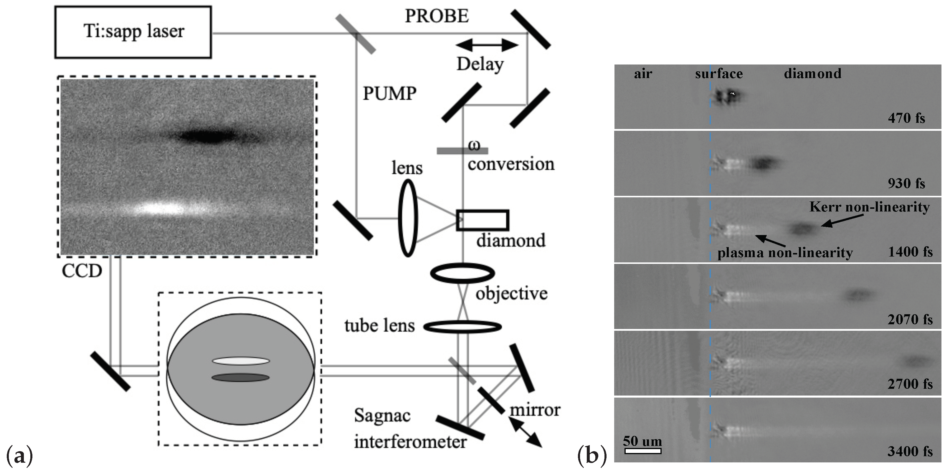
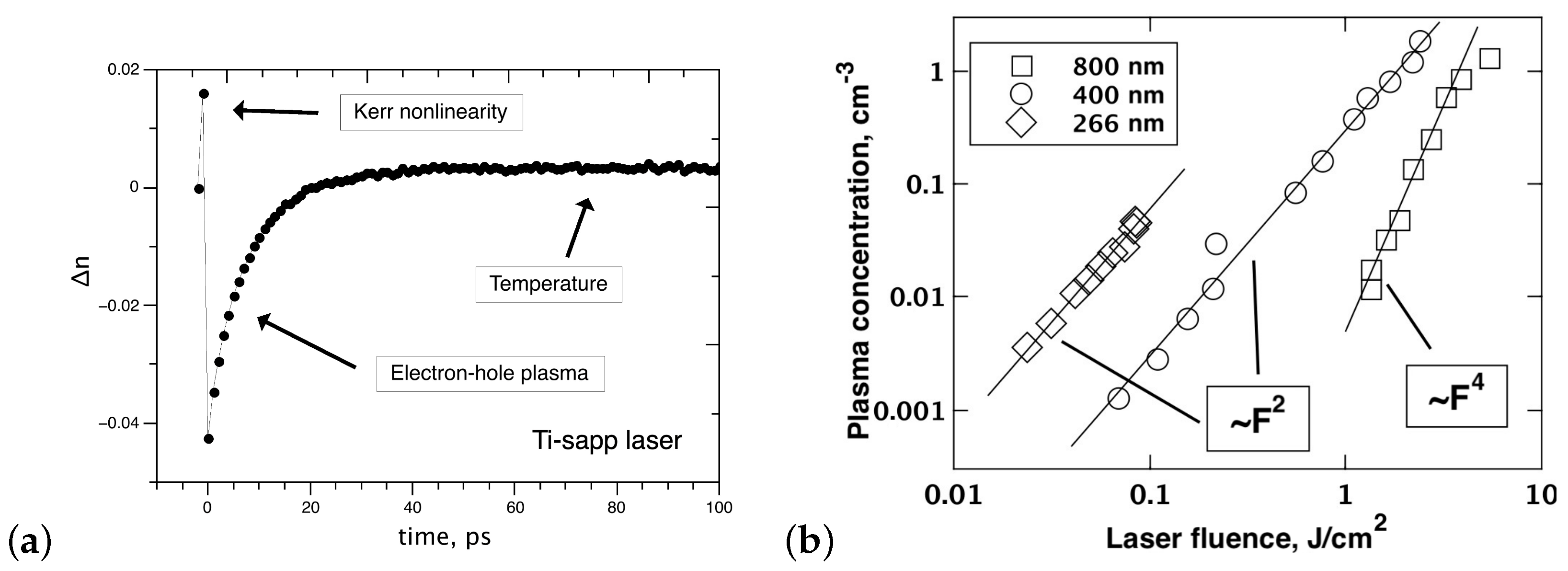
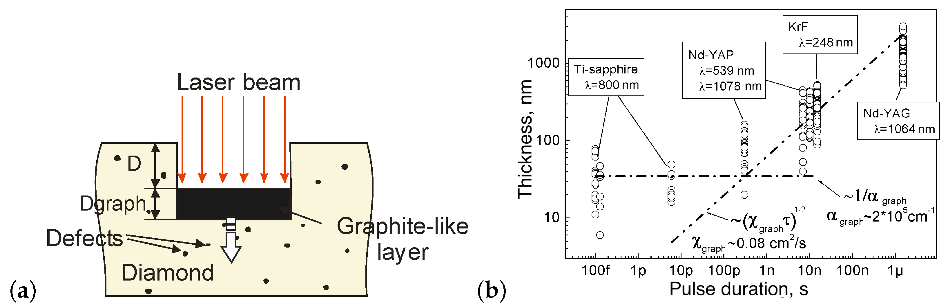
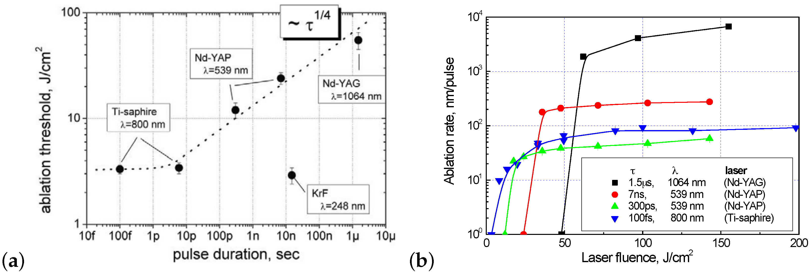
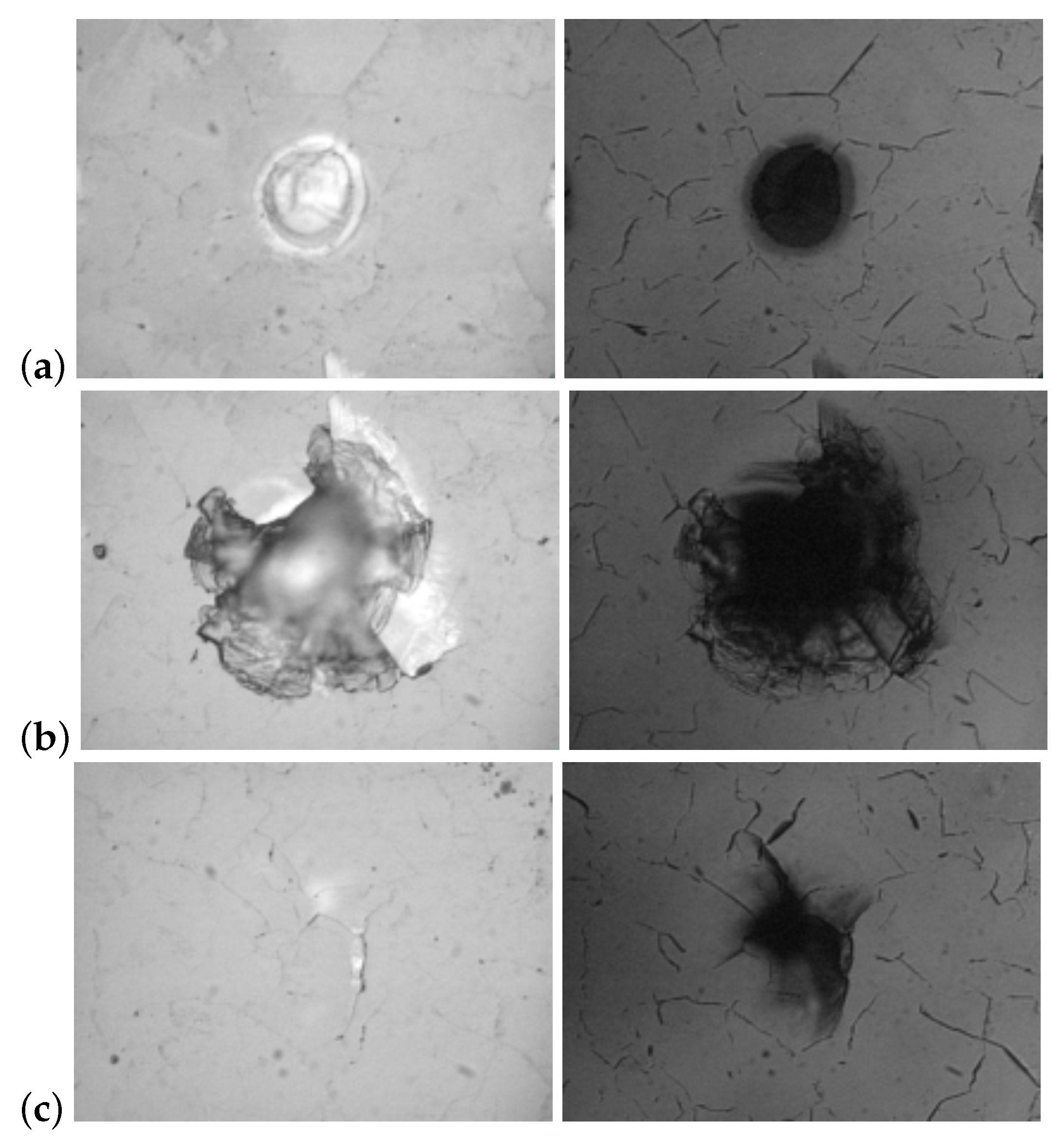
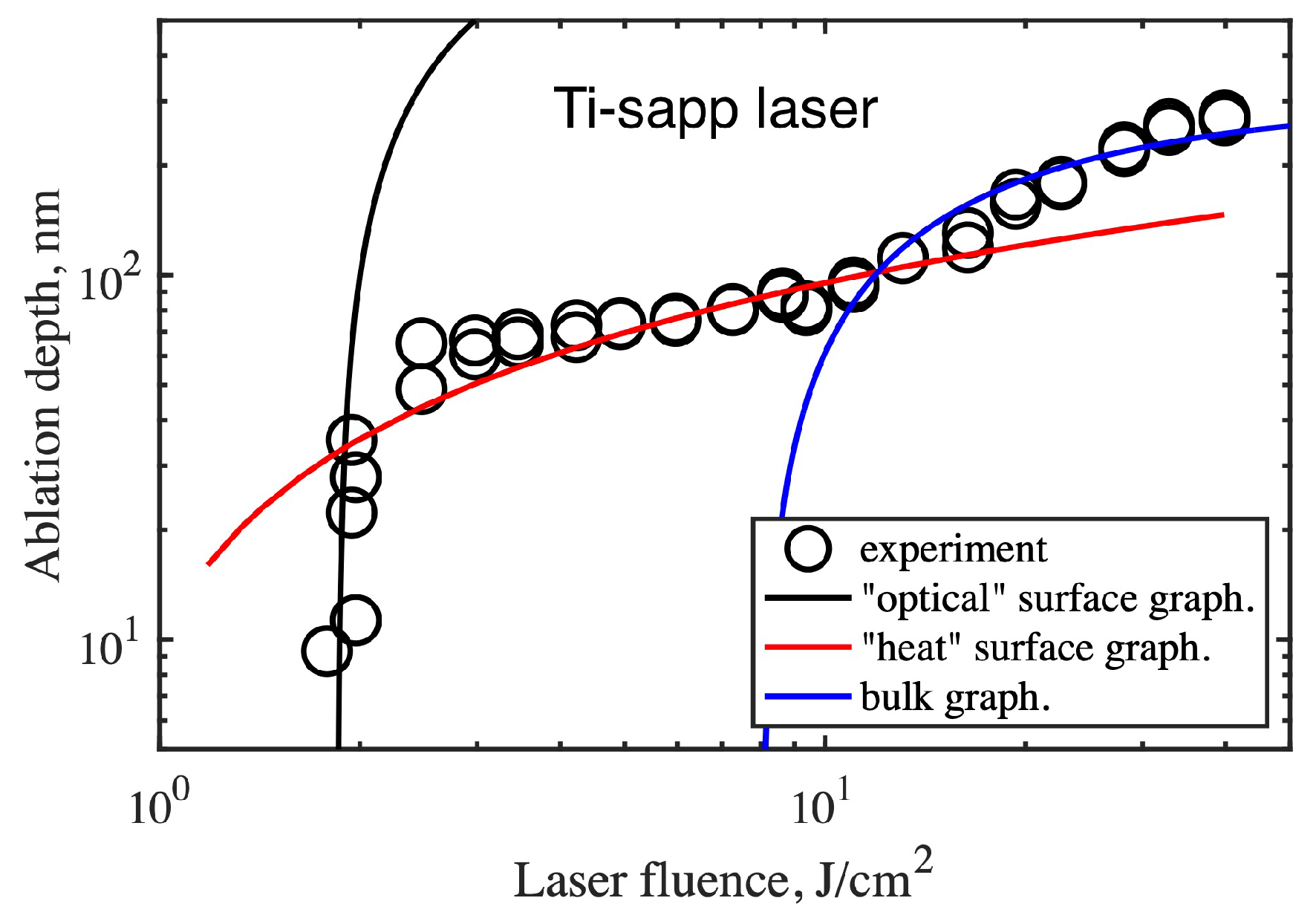
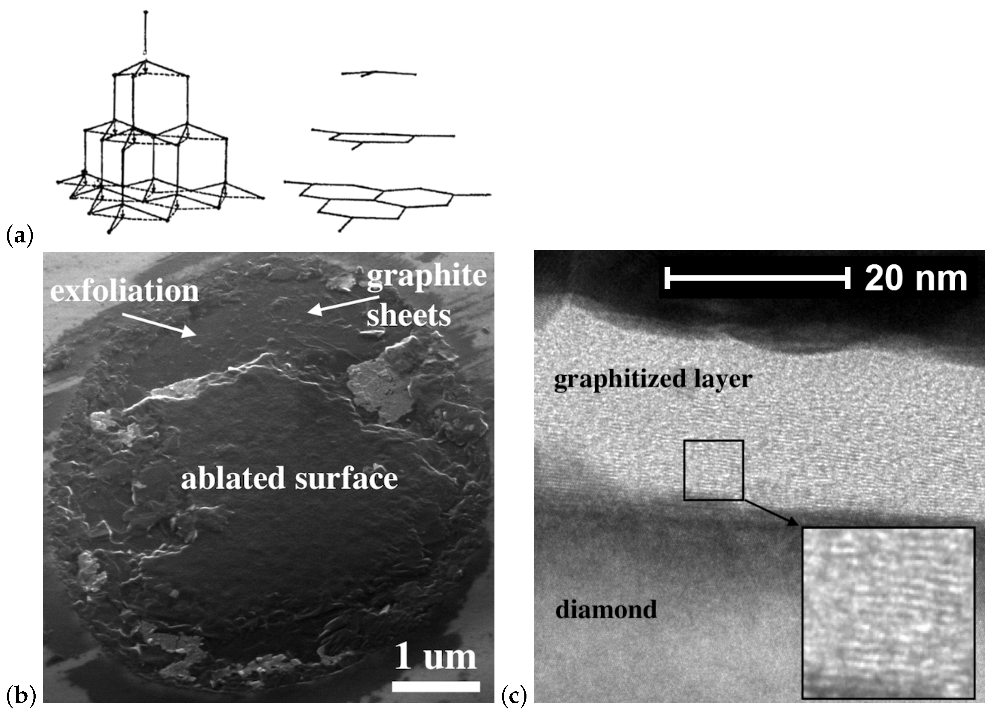
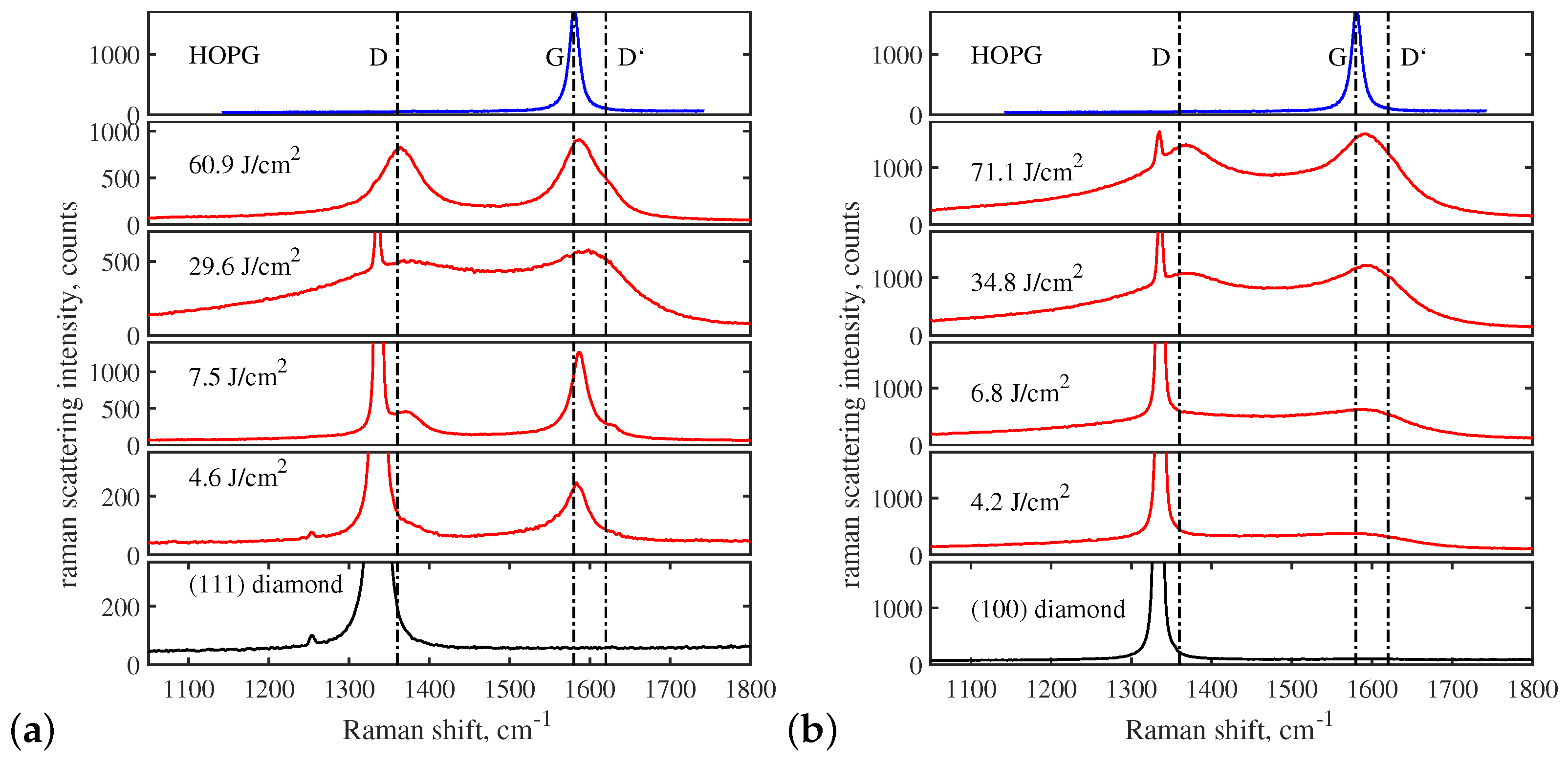
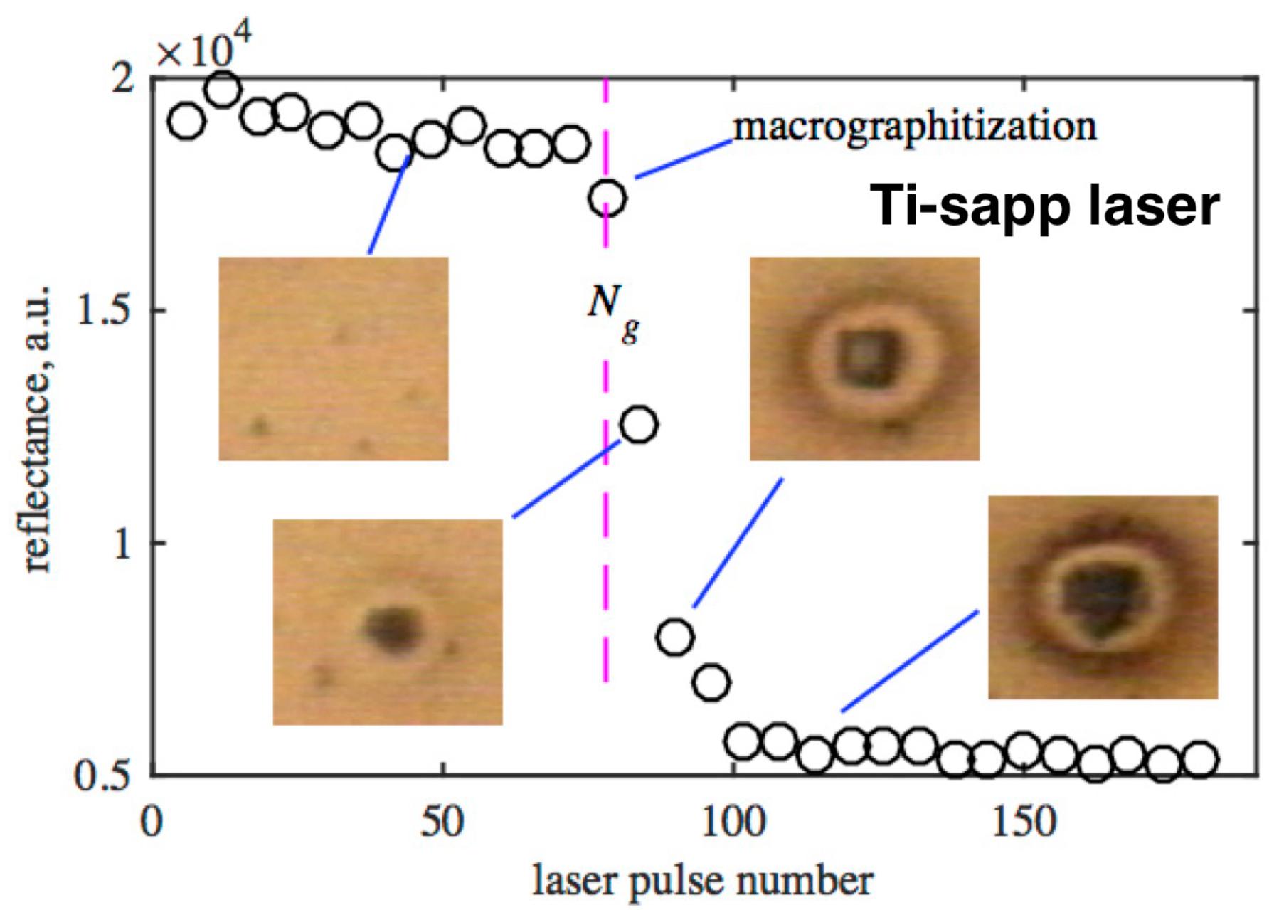
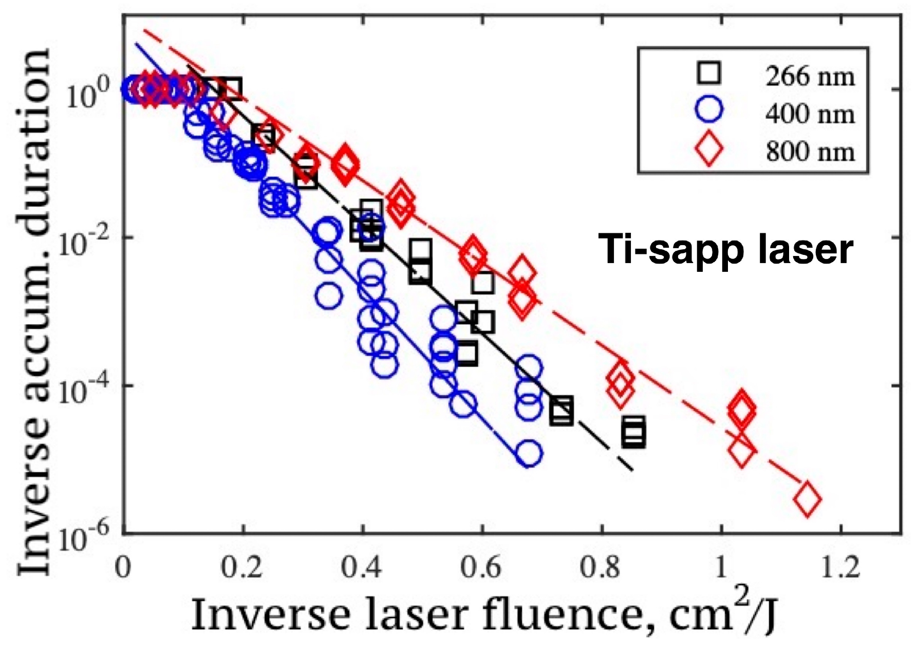
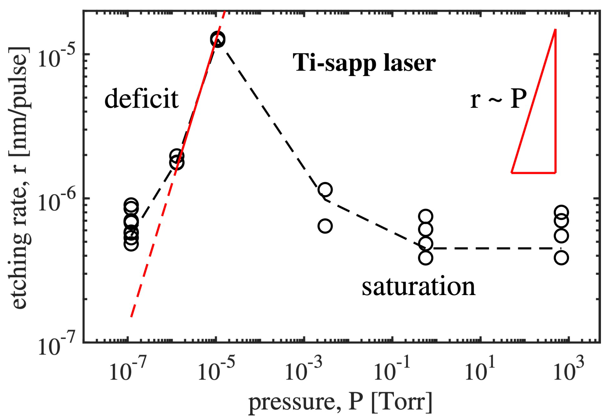
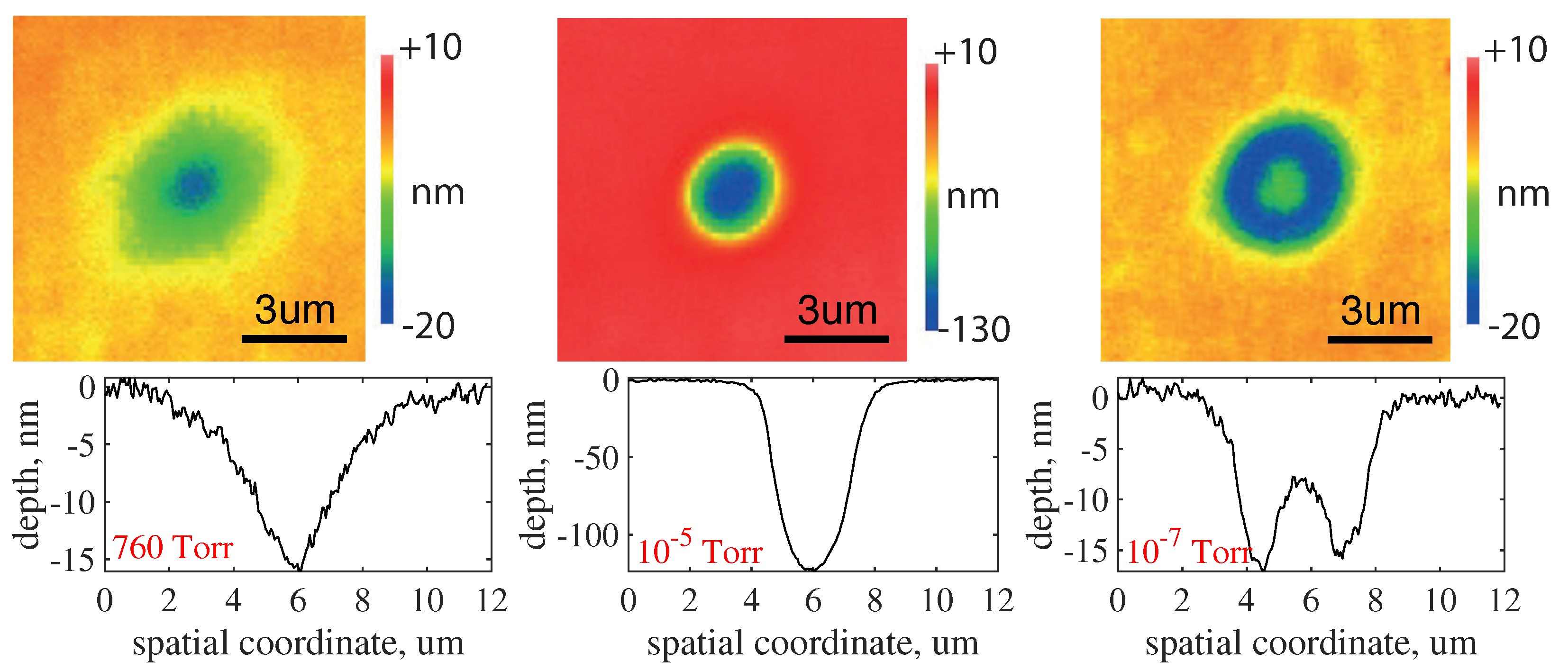
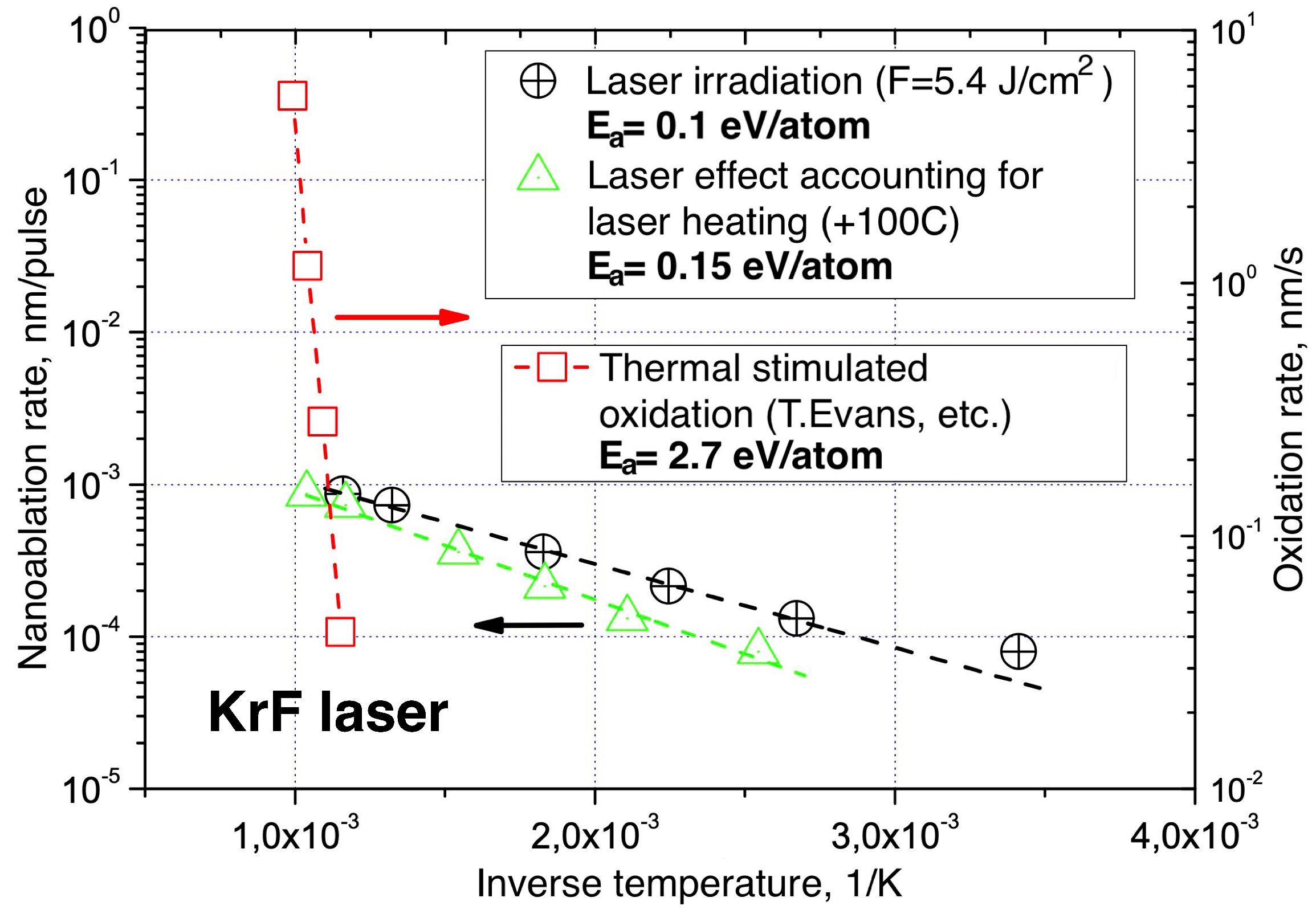
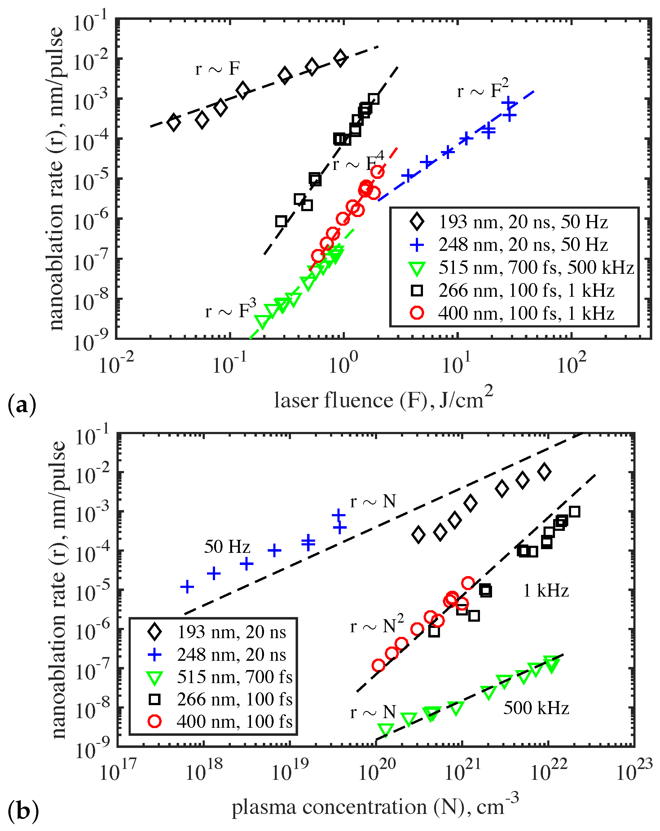
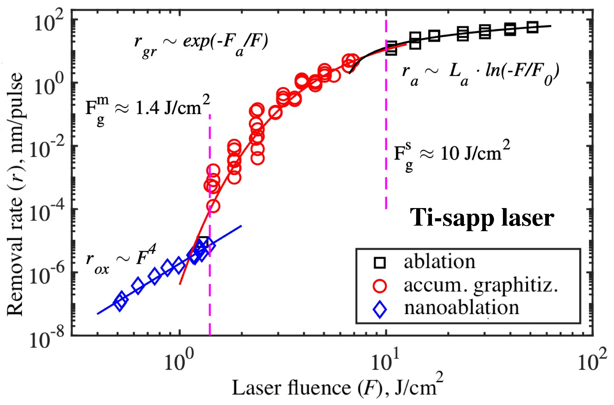
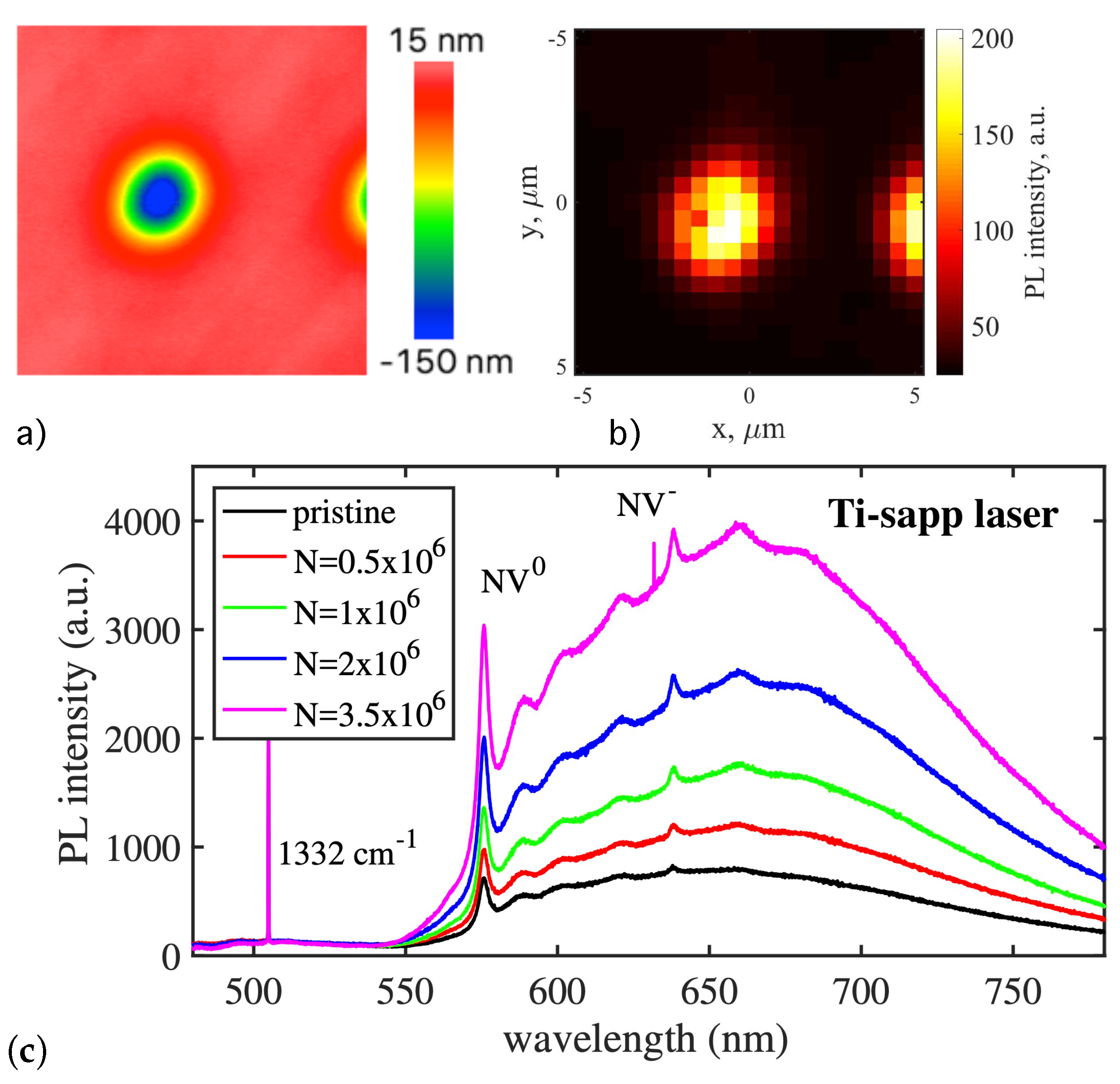
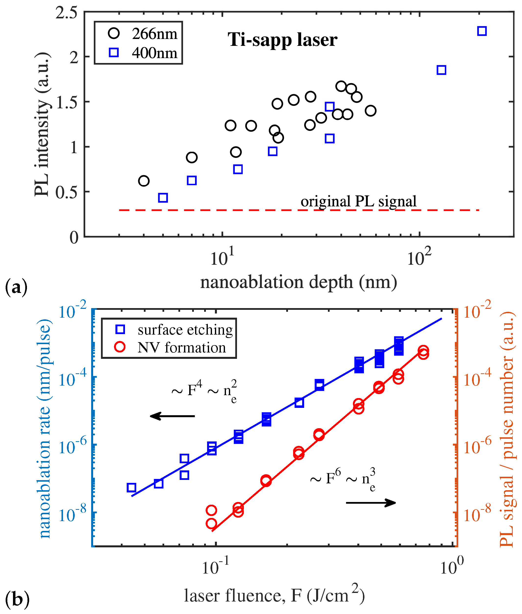
Table 1.
Laser systems used for diamond exposure.
| Laser | Ti:sapp | Nd-YAP | KrF/ArF | Yb:YAG | Nd-YAG |
|---|---|---|---|---|---|
| 100 fs | 300 ps | 15 ns | 400 fs | 1.5 s | |
| 6 ps | 10 ns | 700 fs | |||
| , nm | 800 | 539 | 248 | 515 | 1064 |
| 400 | 1078 | 193 | |||
| 266 | |||||
| f, Hz | 1000 | 10 | 50 | 10 | |
| E, mJ | 1 | 100 | 50 | 0.1 | 100 |
Table 2.
Coefficient of multiphoton absorption in diamond.
| M | (This Work) | (Others) | |
|---|---|---|---|
| 226 | 2 | cm/W | cm/W [47] |
| 400 | 2 | cm/W | – |
| 800 | 4 | cm/W | – |
Disclaimer/Publisher’s Note: The statements, opinions and data contained in all publications are solely those of the individual author(s) and contributor(s) and not of MDPI and/or the editor(s). MDPI and/or the editor(s) disclaim responsibility for any injury to people or property resulting from any ideas, methods, instructions or products referred to in the content. |
© 2023 by the author. Licensee MDPI, Basel, Switzerland. This article is an open access article distributed under the terms and conditions of the Creative Commons Attribution (CC BY) license (https://creativecommons.org/licenses/by/4.0/).
Share and Cite
MDPI and ACS Style
Kononenko, V.V. Modification of Diamond Surface by Femtosecond Laser Pulses. Photonics 2023, 10, 1077. https://doi.org/10.3390/photonics10101077
AMA Style
Kononenko VV. Modification of Diamond Surface by Femtosecond Laser Pulses. Photonics. 2023; 10(10):1077. https://doi.org/10.3390/photonics10101077
Chicago/Turabian StyleKononenko, Vitali V. 2023. "Modification of Diamond Surface by Femtosecond Laser Pulses" Photonics 10, no. 10: 1077. https://doi.org/10.3390/photonics10101077
Note that from the first issue of 2016, this journal uses article numbers instead of page numbers. See further details here.