1. Introduction
Frequency down-converters are critical components in wireless communication and radar systems that transfer the received radio frequency (RF) signals to the intermediate frequency (IF) band to facilitate data acquisition and processing [
1]. To satisfy the demands of the fast mobile traffic growth and the multi-function target detection with an anti-jamming effect, multiple RF bands are simultaneously enabled in such applications [
2,
3]. Therefore, multi-band frequency down-conversion is urgently required to accommodate to the RF signals in different frequency bands. Additionally, the image interference will be introduced in the frequency down-conversion procedure, since both the RF components and the corresponding image components are symmetrical with respect to the frequency of the local oscillator (LO) signal, which are down-converted to an identical IF band. Although the image interference can be avoided by using an electrical bandpass filter to select the target RF signal before down-conversion, it is challenging to achieve a wide-range tunable RF filter with a steep roll-off factor, constraining the operation bandwidth and the flexibility of the system. In fact, electrical mixers based on either Hartley or Weaver architecture are effective for realizing frequency down-conversion with image rejection [
4,
5]. Therefore, the crucial point of the Hartley method is to obtain a pair of IF signals with an orthometric characteristic, which can be realized by using two parallel electrical mixers to mix either a pair of receiving replicas in quadrature with the LO signal, or a pair of LO signals in quadrature with the received signal. However, due to the limited octave and the high nonlinearity in the electronic devices, the operation bandwidth of a single electrical mixer with image rejection is not in a position to cover multiple frequency bands.
Microwave photonic technology is recognized as a promising candidate to circumvent the electronic bottleneck resulting from its large operation bandwidth. Most of the broadband photonic-assisted frequency down-conversion schemes are realized based on electro-optic modulation, where the IF signal is acquired through mutual beating between the specific modulation sidebands corresponding to the RF signal and the LO signal at a photodetector. Under such a construction, the orthometric characteristic for eliminating the image interference can be introduced by employing either the optoelectronic method or the all-optical method [
6,
7,
8,
9,
10,
11,
12,
13,
14,
15,
16,
17,
18,
19,
20,
21,
22,
23,
24,
25,
26,
27,
28,
29,
30,
31]. In the optoelectronic-based scheme, a pair of RF/LO signals in quadrature are firstly produced by using an electrical 90° hybrid coupler (HC). Then, a pair of orthometric IF signals are obtained after photodetection. Thus, the image components can be suppressed after the quadrature coupling of the two orthometric IF signals from the parallel photonic links [
6,
7,
8]. As a comparison, the 90° phase difference between the parallel links can also be produced in an all-optical way, such as by adjusting the direct-current (DC) voltage of the electro-optic modulator [
9,
10,
11,
12], tuning the polarization controller (PC) after polarization division multiplexing [
13,
14,
15,
16,
17,
18,
19,
20,
21], and adopting a 90° optical HC [
22,
23,
24,
25,
26,
27,
28,
29]. All of these frequency mixers realize excellent image rejection results. Nevertheless, in order to remove the undesirable modulation sidebands, optical spectrum selectors, such as an optical filter, a wavelength division multiplexer, and an asymmetric Mach–Zehnder interferometer, are essential for decreasing the operation bandwidth and the flexibility of the all-optical-based scheme [
9,
10,
11,
12,
13,
14,
15,
16,
17,
18,
19,
25,
26,
27,
28,
29]. The filter-free mixer with image rejection has already been proposed using a dual-parallel Mach–Zehnder modulator (DPMZM), with the assistance of an electrical 90° HC, for the purpose of suppressing the undesired sidebands via carrier-suppressed single-sideband (CS-SSB) modulation [
20,
21,
22,
23,
24]. In [
30], a compact scheme using a multi-functional mixer with image rejection, spur suppression, and dispersion immunity has been demonstrated, without using any optical spectrum selectors. Although existing image-rejection mixers based on microwave photonic technology are capable of realizing the image rejection for an RF signal in a large frequency range, the wideband characteristic of the down-conversion relies on a wide-range tunable LO signal generator, which inevitably increases the complexity of the receiver.
In this paper, a multi-band frequency down-conversion scheme is proposed and experimentally demonstrated based on photonic sampling. This scheme is featured with image rejection, and it does not require any electrical or optical filter. Benefiting from photonic sampling via an ultra-short optical pulse train, only a low-frequency LO signal is needed to achieve multi-band frequency down-conversion in a large frequency range. In the experiment, multi-band RF signals in the frequency range of 6 GHz to 39 GHz are simultaneously down-converted to the IF band below 4 GHz by using an LO signal at 8 GHz. Through using digital signal processing to compensate for the amplitude and phase mismatch between two parallel branches, the image components in the whole operation bandwidth are suppressed to be below the noise floor. In addition, the capacity of real-time image rejection is also verified in the analog domain.
2. Operation Principle
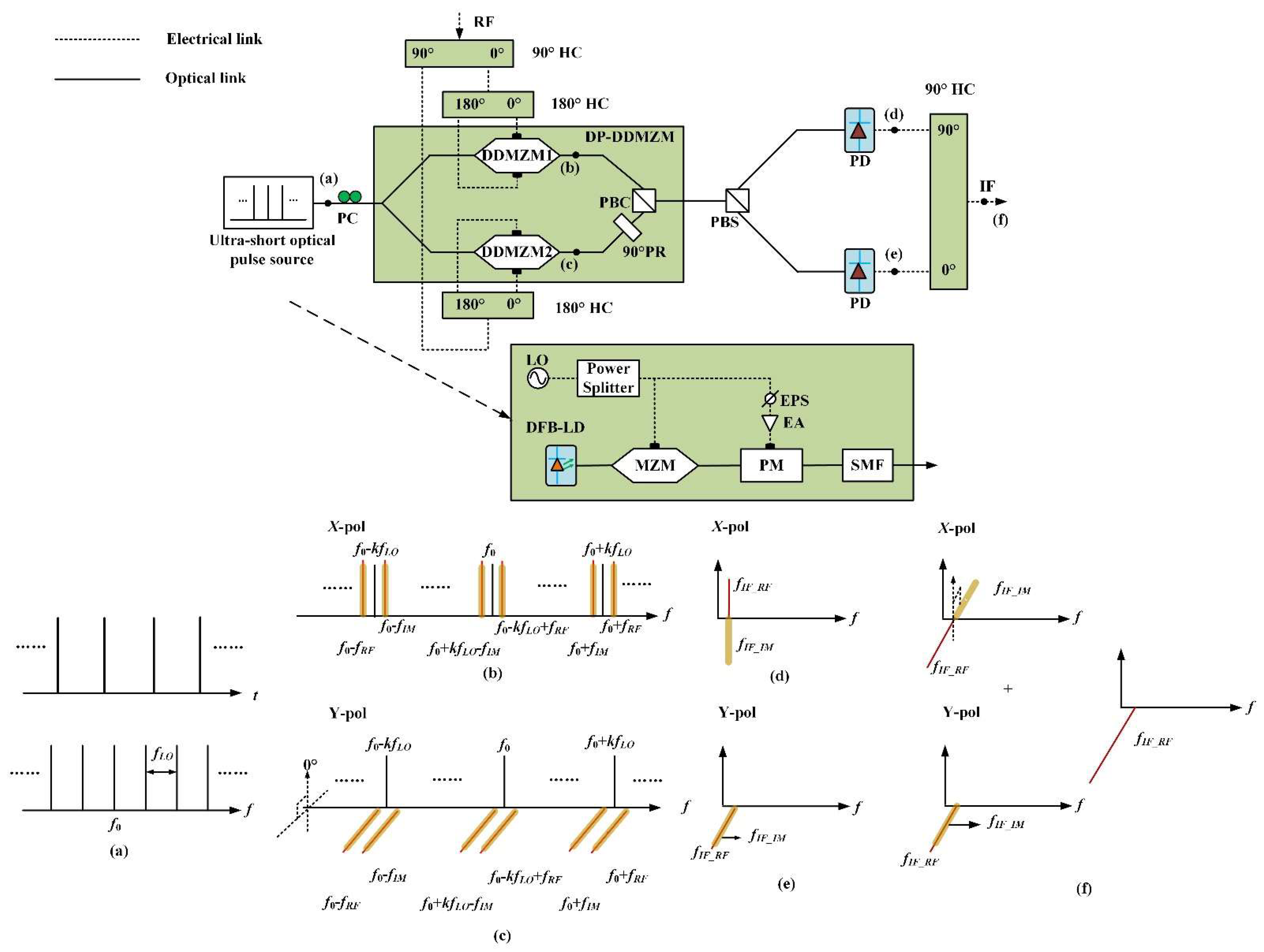
Figure 1 shows the schematic diagram of the proposed filter-free image-rejected multi-band frequency down-conversion based on photonic sampling. To facilitate understanding the signal conversion process in the optical and electrical domains,
Figure 1a–f shows the signal waveforms and spectra at the corresponding nodes of the system. The ultra-short optical pulse train used for photonic sampling is generated by a cavity-less optical pulse source. The optical source is composed of a microwave frequency synthesizer, a power divider, an electrical amplifier (EA), an electrical phase shifter (EPS), a distributed feedback laser diode (DFB-LD), an electro-optic Mach–Zehnder modulator (MZM), an electro-optic phase modulator (PM), and a spool of single-mode fiber (SMF), as shown in
Figure 1. The operation principle of the cavity-less optical pulse source is briefly introduced as follows. The LO signal at
fLO from the microwave frequency synthesizer is divided into two branches. One part of the LO signal is modulated onto the continuous-wave (CW) light at
f0 from the DFB-LD via the MZM biased at its linear transmission point to produce an initial optical pulse train with a repetition rate of
fLO, where the peak-to-peak voltage of the LO signal is set to be almost equal to the half-wave voltage of the MZM. The other part of the LO signal is amplified and used to drive the PM, where its phase is properly adjusted through the EPS until the temporal profile of the LO signal aligns with the optical pulse in the time domain. Under this condition, an approximate quadratic phase is introduced into each optical pulse. After propagation through a spool of SMF with a proper group velocity dispersion (GVD) value, the chirped optical pulse train is compressed into an ultra-short optical pulse train with a repetition rate of
fLO, whose spectrum is an optical comb centered at
f0, and with a frequency interval of
fLO, as shown in
Figure 1a. As for the frequency down-conversion system, the generated ultra-short optical pulse train enters a dual-polarization dual-drive Mach–Zehnder modulator (DP-DDMZM), where the RF signal to be down-converted is optically sampled via linear electro-optic modulation. Thus, the RF signal at
fRF and the possible image signal at
fIM (supposing
fRF >
fIM) are divided into two parts with identical amplitudes, but with a 90° phase difference, by using an electrical 90° HC. Then, each part of the signal is copied into two replicas with a reversed phase by using an electrical 180° HC and is applied to DDMZM1 and DDMZM2, respectively. Both DDMZM1 and DDMZM2 work at the quadrature point to achieve linear electro-optic modulation. From the perspective of spectrum, the signal to be down-converted is modulated onto each tooth of the optical frequency comb at
f0 +
kfLO (
k = 0, ±1, ±2…), and the modulated optical spectra in two polarizations are presented in
Figure 1b,c. After passing through a 90° polarization rotator (PR), the sampled optical pulse trains from the two DDMZMs are polarization multiplexed using a polarization beam combiner (PBC). Then, the sampled optical pulse trains are polarization demultiplexed via a polarization beam splitter (PBS) and are detected by using two photodetectors (PDs), respectively. The RF signal and the possible image signal are down-converted to the IF band, and the electrical spectra are shown in
Figure 1d,e. Here,
fIF_RF and
fIF_IM denote the IF signals down-converted from the RF signal and the image signal, respectively. The phase difference of the IF signals down-converted from the RF signal between the two channels is −90°, while it is 90° for the IF signals down-converted from the possible image signal. Through combining the two groups of the IF signals via an electrical 90° HC, the IF signals down-converted from the possible image signal cancel each other, while the IF signals down-converted from the RF signal superpose in phase, as shown in
Figure 1f. Hence, filter-free image-rejected frequency down-conversion is achieved. In addition, due to the use of photonic sampling, RF signals in a large frequency range can be simultaneously down-converted to the Nyquist bandwidth below
fLO/2. Therefore, the proposed scheme can realize filter-free image-rejected frequency down-conversion, in which only a low-frequency LO signal is required.
Mathematically, the MZM and the PM in the optical pulse source are driven by single-tone microwave signals of
VLO1(
t) =
VLO1·cos(
ωLOt) and
VLO2(
t) =
VLO2·cos(
ωLOt), respectively. Here,
VLO1 and
VLO2 are the voltage magnitudes of the microwave signals applied to the MZM and the PM, respectively, and
ωLO is the angular frequency of the microwave signal. Through properly tuning the EPS, the signal profile applied to the PM aligns with each optical pulse. After propagation through a spool of SMF, the optical field of the ultra-short optical pulse train output from the cavity-less optical pulse source can be written as [
31]
where
E0 =
E·
ejw0t is the optical filed of the CW light from the DFB-LD.
m1 =π
VLO1/
Vπ1 and
m2 =π
VLO2/
Vπ2 are the modulation indices of the MZM and the PM, respectively, where
Vπ1 and
Vπ2 are the half-wave voltages of the MZM and the PM, respectively.
φ1 = π
Vbiasup/
Vπ1_DC is the bias phase shift of the MZM, where
Vbias1 and
Vπ1_DC are the bias voltage and the DC half-wave voltage of the MZM, respectively.
Jn(
x) is the
nth-order Bessel function of the first kind.
L and
β2 are the length and the GVD coefficient of the SMF, respectively. The signal to be processed, i.e.,
Vsig(
t) =
VRF·cos(
ωRFt) +
VIM·cos(
ωIMt), is applied to the DP-DDMZM and optically sampled by the ultra-short optical pulse train (assuming
ωRF >
ωIM), where DDMZM1 and DDMZM2 are biased at their quadrature points.
ωRF and
VRF are the angular frequency and the voltage magnitude of the RF signal, respectively.
ωIM and
VIM are the angular frequency and the voltage magnitude of the possible image signal, respectively. The output optical field of the DP-DDMZM in the time domain can be expressed as
where
m3 = π
VRF/
Vπ and
m4 = π
VIM/
Vπ are the modulation indices corresponding to the RF signal and the image signal in the DP-DDMZM, respectively.
Vπ is the half-wave voltage of the DP-DDMZM. Under small-signal modulation, the output optical field of the DP-DDMZM can be simplified as
where
a,
b, and
c are the amplitude coefficients of the optical carrier, the 1st-order modulation signal corresponding to the RF signal, and that corresponding to the image signal, respectively. After polarization demultiplexing and photodetection, the output currents from the two photodetectors can be calculated as
where
AN is the amplitude of the frequency-multiplied components at
NωLO.
Q1 and
Q2 are the amplitude coefficients of the IF components generated from the beating between the RF/image signal modulation sidebands and the corresponding frequency teeth of the optical pulse source, respectively. Equation (4) indicates that the RF signals and the corresponding image signals in the two branches are simultaneously down-converted to the IF band below
fLO/2 when
. Thus,
represents the rounding down of
x. Although the IF signals down-converted from the RF and the image signals at
fIF_RF and
fIF_IM are aliased in each branch, with an identical frequency and amplitude, their phases are ±90°, respectively. Therefore, after combining the two output optical currents via an electrical 90° HC to introduce a 90° phase shift in the first branch, the output current of the 90° HC is calculated as
It can be seen from Equation (5) that the IF signal down-converted from the image component is eliminated by coupling the two samples from the two branches with a reversed phase. Additionally, the multiple-frequency band signals can be simultaneously down-converted to the IF band below fLO/2, which benefits from the optical sampling scheme by using an ultra-short optical pulse train. Therefore, the RF signal at the high frequency band can be down-converted to the IF band, free of image interference and without the requirement of a wide-range tunable LO signal generator. In addition, if the signal at the symmetrical frequency band with respect to NfLO is desired (i.e., ωRF < ωIM), the interference of the image frequency component can also be suppressed by exchanging the input ports of the electrical 90° HC for quadrature coupling, i.e., the output current of the 90° HC equals Ix(t) + Iy(t)·ejπ/2.
3. Simulation and Discussion
Numerical simulation is implemented to verify the feasibility of realizing broadband image-rejected down-conversion and optimize the frequency response flatness of the proposed down-conversion scheme. Here, the frequency response of the down-conversion system depends on the frequency response of the employed devices and the characteristics of the sampling optical pulse train. In the simulation, special attention is paid to the optimization of the parameter setting for the cavity-less optical pulse source. Therefore, for simplicity, the extinction ratio of the PBS, the bandwidth of the photodetectors, and the insertion loss of all devices are not taken into account in the simulation. This simplification has no influence on the evaluation of the frequency response flatness optimization. The ultra-short optical pulse source is composed of a 1550-nm DFB-LD with an output power of 16 dBm, an MZM and a PM with 3-dB bandwidths larger than 40 GHz, a spool of SMF with a GVD value of 41.4 ps/nm, and a microwave frequency synthesizer at 8 GHz. The MZM is biased at its quadrature point, and the modulation indices of the MZM and the PM are set to be 0.5π and 3π, respectively. The modulation index of the PM corresponds to the GVD value of the SMF for optimal pulse compression. The responsivity of the two photodetectors is 0.6 A/W.
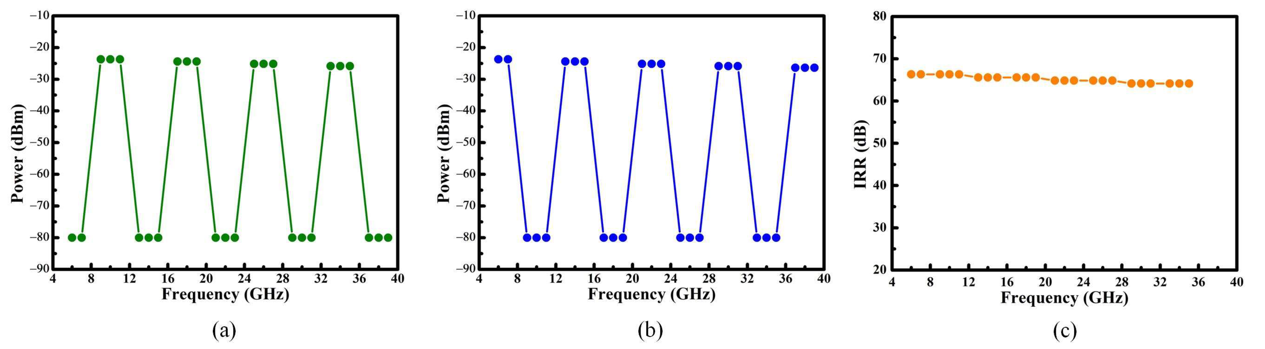
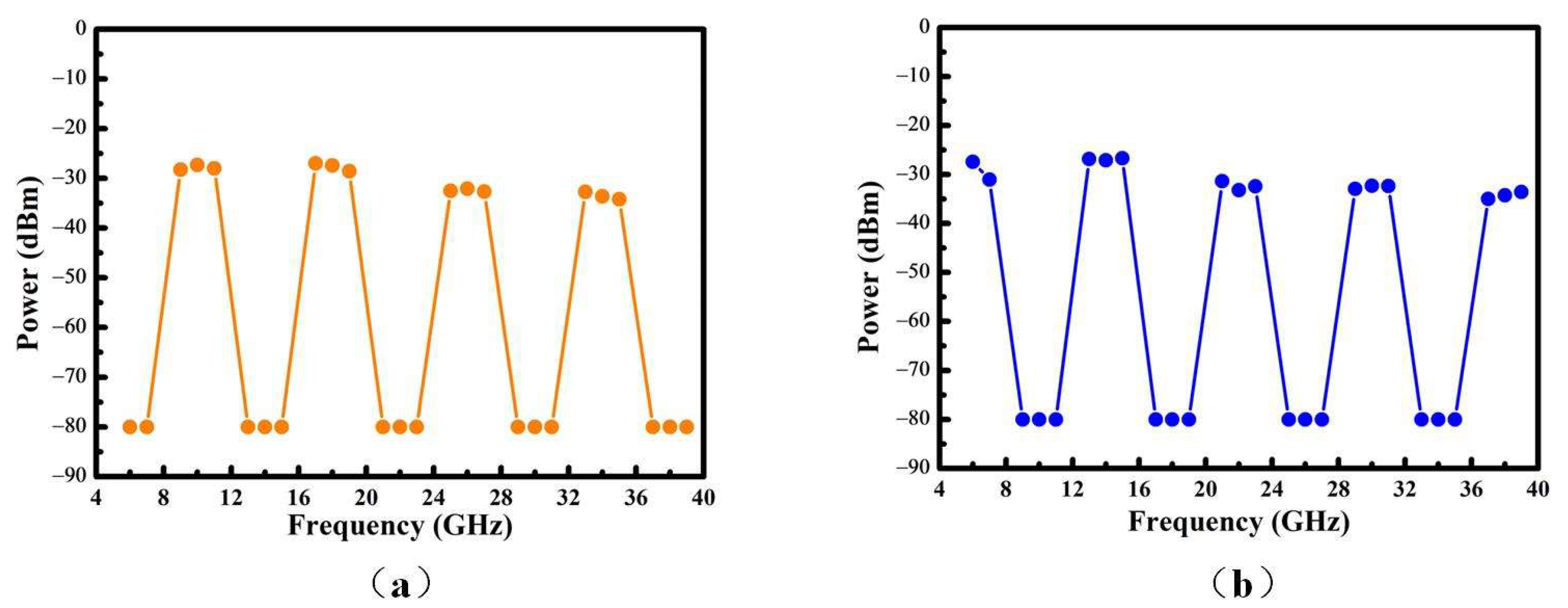
A single-tone microwave signal in the frequency range of 6 GHz to 39 GHz and with a power of 10 dBm is applied to the DP-DDMZM via three electrical HCs to act as the signal to be processed. After being optically sampled by the ultra-short optical pulse train, the input signal is down-converted to the IF band below 4 GHz.
Figure 2a,b show the output power of the IF signals down-converted from the input signal, with its frequency varying from 6 GHz to 39 GHz. In
Figure 2a,b,
Ix(
t)
·ejπ/2 +
Iy(
t) and
Ix(
t) +
Iy(
t)
·ejπ/2 are used to achieve quadrature coupling, respectively. The simulation results indicate that the power fluctuation of the IF signal is 2.69 dB within the operation frequency range of 6 GHz to 39 GHz. Meanwhile, the desired frequency bands can be switched by exchanging the IF quadrature coupling method.
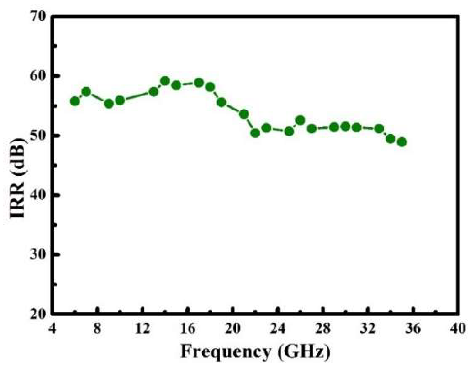
Figure 2c exhibits the image rejection ratios (IRRs) of the mixer with respect to the input signals at different frequencies, which are larger than 60 dB in the frequency range of 6 GHz to 35 GHz.
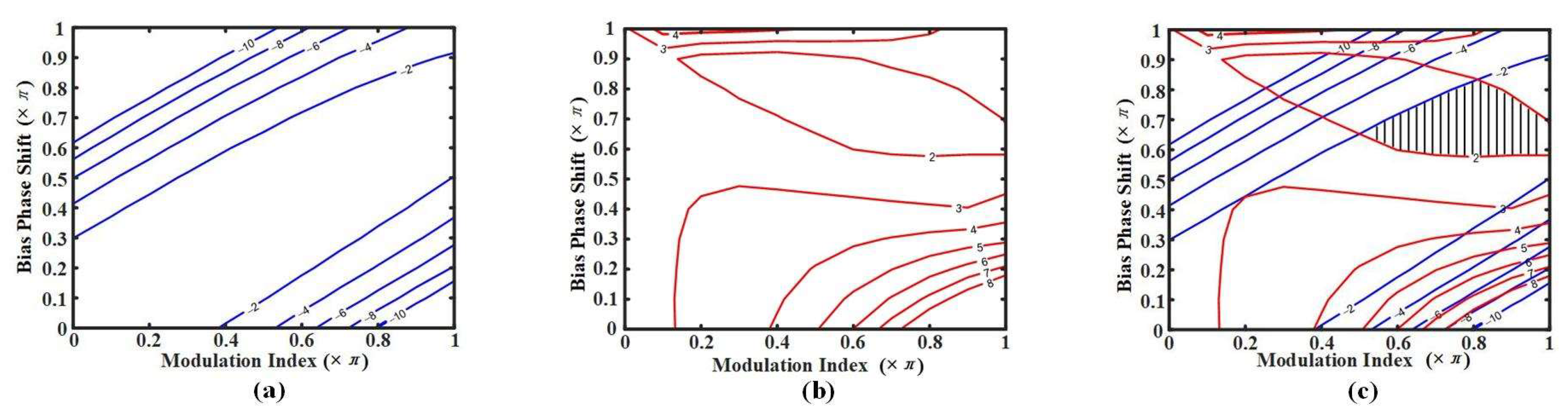
Numerical analysis is also implemented for achieving a broadband down-conversion. As shown in Equation (5), the amplitude of the IF signals is proportional to the amplitude of the frequency-multiplied component from the LO signal, with corresponding multiples. In addition, it can be seen from Equations (1)–(4) that the amplitude coefficient
AN is dependent on the parameters of the ultra-short optical pulse source, including the modulation indices of the MZM and the PM, the bias phase shift of the MZM, the GVD value of the SMF, and the frequency of the LO signal. Therefore, the power fluctuation of the IF signals can be optimized through the parameters of the ultra-short optical pulse source. For an ultra-short optical pulse source with a specific repetition rate, the modulation index of the PM needs to be set as high as possible for obtaining a broadband optical spectrum. Consequently, the GVD value of the SMF is determined accordingly. In the simulation, the power fluctuation of the IF signals down-converted from multiple frequency bands is evaluated under the condition of various modulation indices and bias phase shifts of the MZM.
Figure 3a shows the power contour map of the 5th-order multiplied-frequency component at 40 GHz, where the power of the 5th-order multiplied-frequency component under the condition of
m1 = 0.5π and
φ1 = 0.5π is used as the reference value for normalization.
Figure 3b shows the contour map of the power fluctuation between the 1st-order multiplied-frequency component at 8 GHz and the 5th-order multiplied-frequency component at 40 GHz.
Figure 3c presents the overlapping contour map shown in
Figure 3a,b. Here, the slash area corresponds to the parameter setting of the MZM to simultaneously obtain a power fluctuation below 2 dB and a normalized power of the 5th-order multiplied-frequency component at 40 GHz higher than −2 dBm. This is the optimal parameter setting for achieving broadband down-conversion.
4. Experiment Results and Discussion
A proof-of-concept experiment is carried out to verify the feasibility of the proposed scheme. The ultra-short optical pulse source is constructed by employing a DFB-LD (Pure photonics PPCL500) at 1550 nm and with an output power of 16 dBm, a 40-Gb/s MZM (Photline, MXAN-LN-40-00-P-P-FA-FA), a 20-Gb/s PM (EOSpace, PM-SSEE-20-PFA-PFA-UV), a spool of 2.47-km-long SMF (YOFC G652D) with a GVD value of 41.4 ps/nm, and a self-developed dual-output microwave signal source with an output frequency of 8 GHz. Two pairs of electrical attenuators and RF power amplifiers are used to tune the output power of the two LO signals. Meanwhile, an EPS with a tuning range from 0° to 180° is adopted to set the phase difference of the LO signals between two outputs of the microwave signal source. In the experiment, the modulation index of the PM is set to be 3π, and the modulation index of the MZM varies from 0 to π through controlling the output power of the two LO signals, respectively. The signal profile applied to the PM is adjusted to align with each optical pulse through tuning the EPS. The input RF signal is optically sampled by the ultra-short optical pulse train via a DP-DDMZM (Fujitsu, FTM7980EDA) with a 3-dB bandwidth of 30 GHz. Here, an electrical 90° HC (Marki, QH0440) with an operation frequency range from 4 GHz to 40 GHz and two electrical 180° HCs (Gwave, GHC-180-060400) with an operation frequency range from 6 GHz to 40 GHz are used to load the RF signal onto the ultra-short optical pulse train. A PBS with an extinction ratio of 31 dB is applied to achieve polarization demultiplexing. Two photodetectors (Discovery DSH-10H) with a 3-dB bandwidth of 40 GHz and a responsivity of 0.65 A/W are employed to detect the IF signals.
To verify the optimized parameter setting for the ultra-short optical pulse source, the generated ultra-short optical pulse train is directly detected by using a broadband PD (Discovery DSH-10H), where the generated electrical spectrum is measured using an electrical spectrum analyzer (ESA, R&S FSW67).
Figure 4a,b shows the normalized power of the 5th-order multiplied-frequency component at 40 GHz, and the power fluctuation between the 1st-order multiplied-frequency component at 8 GHz and the 5th-order multiplied-frequency component at 40 GHz, respectively, under different bias phase shifts of the MZM. The modulation index of the MZM is set to be 0.7π. It can be seen from
Figure 4 that the variation tendency of the measured power for the multiplied-frequency component at 40 GHz and the power fluctuation of the 1st-order and the 5th-order multiplied-frequency component coincide with the simulation results shown in
Figure 3a,b, respectively. Specifically, the optimal parameter setting for the MZM to achieve broadband down-conversion with a higher output power is a modulation index of 0.7π and a bias phase shift of 0.7π. Under the optimal parameter setting, the power flatness of the generated electrical frequency comb is 5.21 dB, which is deteriorated by approximately 3 dB compared with the simulation results due to the frequency response degradation of the PD.
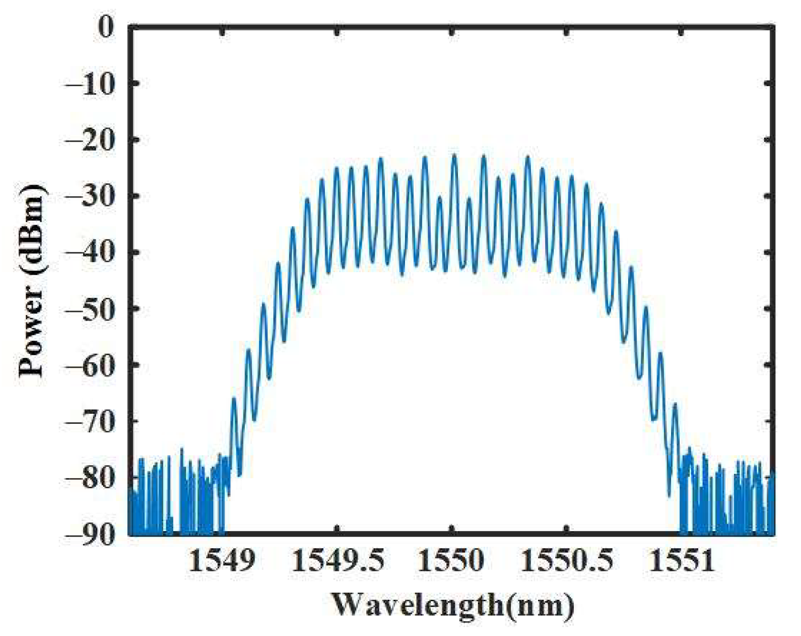
Figure 5 shows the optical spectrum of the generated ultra-short optical pulse train under the optimal parameter setting. The 3-dB bandwidth of the optical pulse source is measured to be 0.512 nm, indicating that the optical pulse train contains nine optical frequency comb teeth in its 3-dB bandwidth.
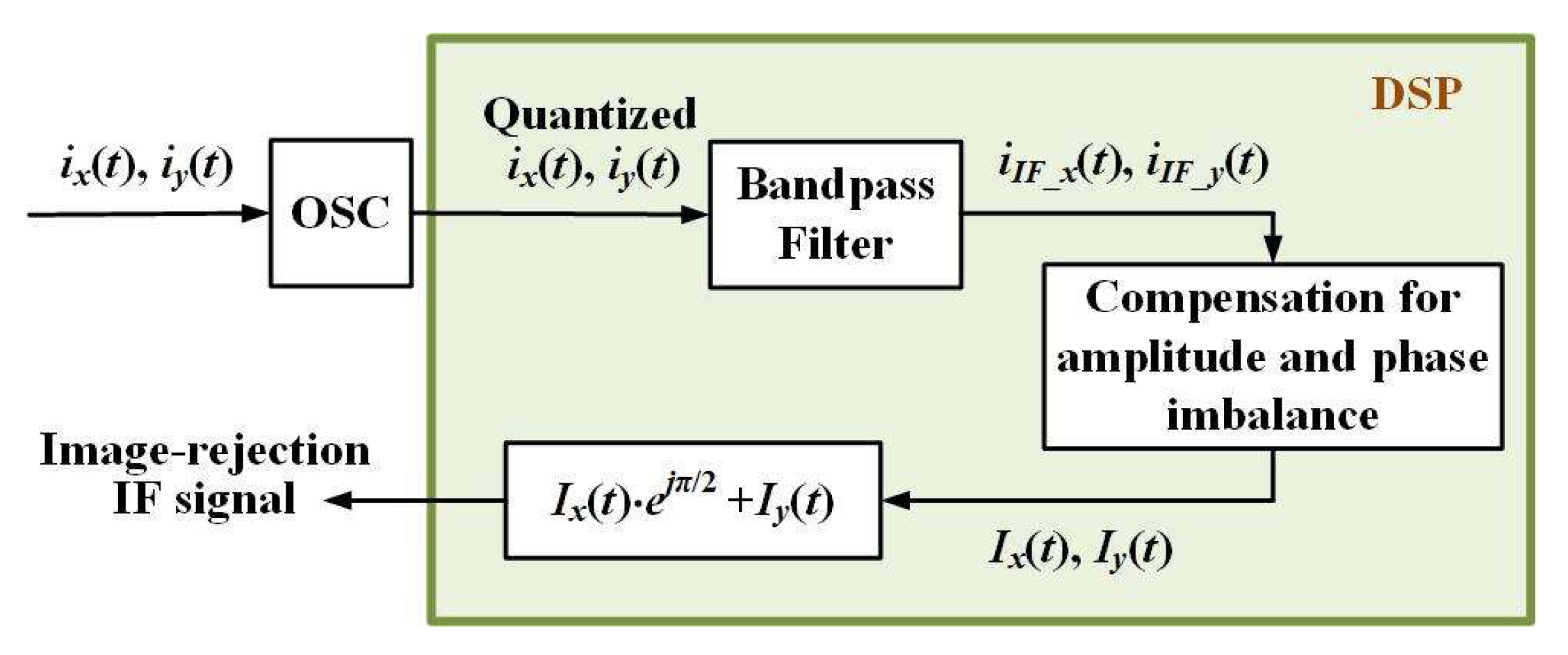
Then, a single-tone RF signal in the frequency range of 6 GHz to 39 GHz and with a power of 15 dBm is generated by using a microwave frequency synthesizer (R&S SMB100A). To boost the RF signal power with a frequency coverage up to 39 GHz, two electrical amplifiers, with operation frequency ranges of 35 MHz to 22 GHz (GT-HLNA-0022G) and 22 GHz to 40 GHz (GT-LNA-2244), are adopted. After being optically sampled by the optimized ultra-short optical pulse train via the DP-DDMZM, the RF signals in the two polarization channels are detected by using two PDs, and then recorded by using a real-time oscilloscope (OSC, LeCrow 816Zi-B) with a sampling rate of 40 GS/s, a 3-dB bandwidth of 16 GHz, and a quantization bit of 8 bits. Additionally, before photodetection, two erbium-doped fiber amplifiers (EDFA, Amonics AEDFA-PA-35-B-FA) are employed to compensate for the insertion loss in the optical links. In order to correct the amplitude and phase imbalance of the signals from the two parallel branches, a compensation operation is implemented via digital signal processing (DSP), and the flow chart of the imbalance compensation is shown in
Figure 6. Initially, the quantized signals from the OSC pass through two bandpass filters, respectively, to pick out the IF signals below 4 GHz. Then, the amplitude imbalance and the phase delay between the two IF signals are evaluated and compensated for in the time domain and in the frequency domain, respectively. Finally, two corrected signals are quadrature combined to obtain the IF signal, free of image interference.
Figure 7a,b shows the output power of the acquired IF signal after DSP operation and quadrature coupling using
Ix(
t)
·ejπ/2 +
Iy(
t) and
Ix(
t) +
Iy(
t)
·ejπ/2, respectively, under various input RF signal frequencies. The measurement results indicate that the 6-dB mixing frequency range is from 9 GHz to 34 GHz, and from 6 GHz to 33 GHz, respectively. The power fluctuation within the frequency range of 6 GHz to 39 GHz is 8.32 dB. Compared with the power fluctuation of 2.69 dB in the simulation, the relatively large power fluctuation in the experiment is attributed to the following four factors, i.e., the electrical spectrum curve of the optical pulse source (~2 dB), the inconsistent gain of the electrical amplifier (~2 dB), and the frequency response degradation of the DP-DDMZM (~3 dB) and that of the three HCs (~3 dB). Using to the measurement results shown in
Figure 7, the IRRs of the mixer with input signals at different frequencies are calculated and presented in
Figure 8. The IRR of the mixer is measured to be larger than 48.91 dB, indicating that the proposed scheme can achieve effective image rejection. In this condition, the IRR of the mixer is restrained by the noise floor of the electrical spectrum, where the noise floor level depends on the acquisition time of 2 μs limited by the storage depth of the OSC (corresponding to a spectral resolution of 500 kHz). In addition, to further improve the IRR, the input optical power of the two PDs should be increased. In our experiment, the input optical power is restrained below −2 dBm due to the damage threshold of the PDs.
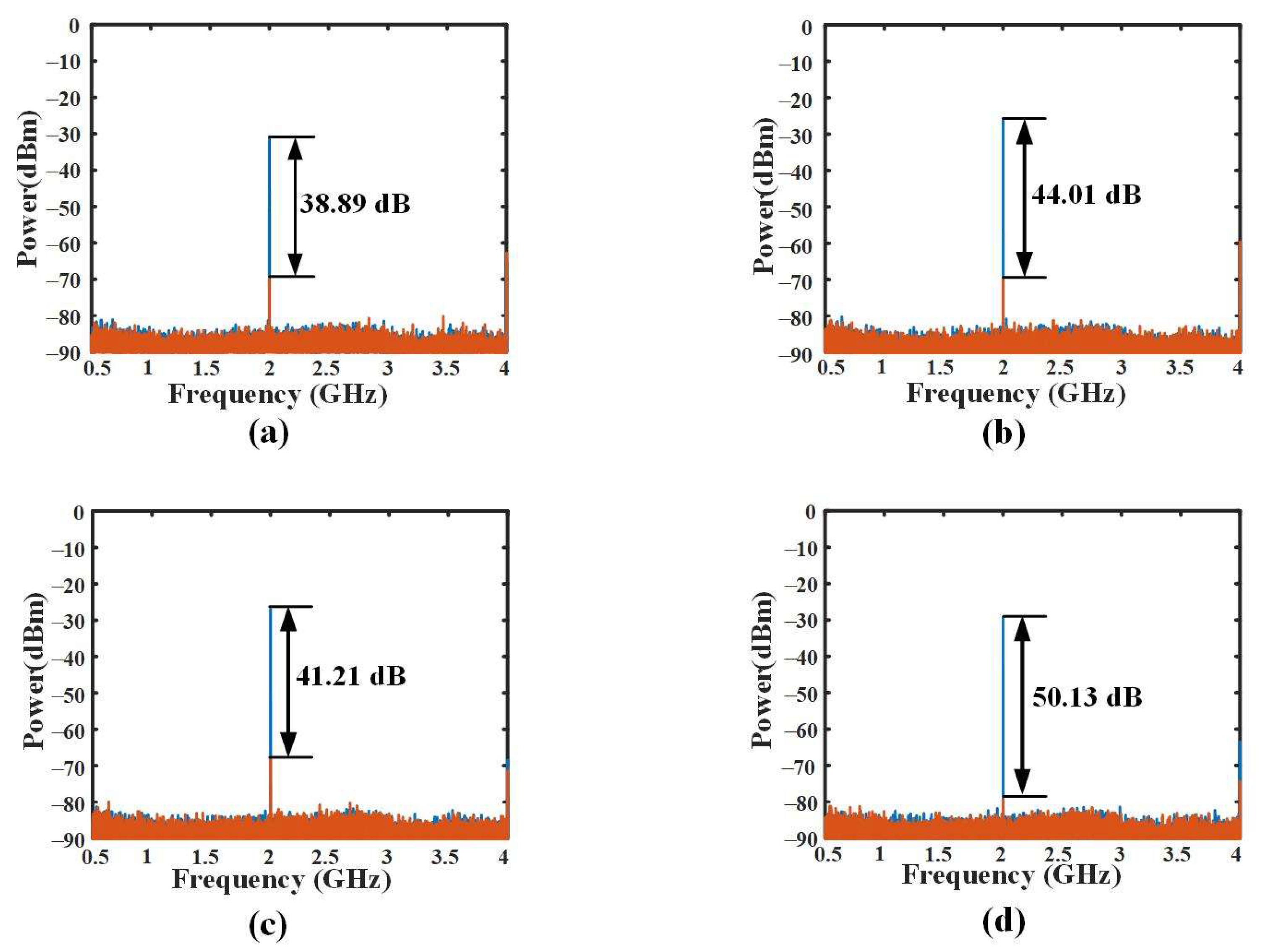
To verify the capacity of real-time image rejection, the correction operation for the amplitude and phase imbalance between the two parallel branches are also implemented in the analog domain using an electrical power attenuator (Rebes, RBS-11-4.3-2) with an operation frequency range from DC to 4.3 GHz and an electrical phase shifter (Connphy, MPS-DC18G-60S) with an operation frequency range from DC to 18 GHz. After compensation, an electrical 90° HC (Marki, QH-0R714), with an operation frequency range from 0.7 GHz to 14.5 GHz, is used to quadrature combine the two parallel signals. The output IF signal is characterized by using an ESA. In this section, the RF signals and their corresponding image signals at four diverse frequency bands and with a power of 11 dBm are generated by the microwave frequency synthesizer and then down-converted through the proposed mixer.
Figure 9a–d shows the electrical spectra of the IF signals down-converted from the RF signals at 10 GHz, 18 GHz, 22 GHz, and 30 GHz, along with those down-converted from their corresponding image signals at 6 GHz, 14 GHz, 26 GHz, and 34 GHz, respectively, where the resolution bandwidth of the ESA is set to be 100 kHz. The IRRs of the signals located at the four diverse frequency bands are 38.89 dB, 44.01 dB, 41.21 dB and 50.13 dB, respectively, indicating that the system is capable of achieving image rejection for multi-band frequency down-conversion. Compared with the results through using DSP, the measured IRRs value after compensation in the analog domain are deteriorated, which is mainly attributed to the residual amplitude and phase deviation between the two parallel branches. Therefore, the residual amplitude deviation is derived from the 0.1 dB tuning step of the electrical power attenuator and the ±0.8 dB amplitude imbalance of the adopted 90° HC. The phase deviation originates from the ±8° phase offset of the adopted 90° HC. In addition, the electrical amplifier used for boosting the input signal is removed, leading to the power reduction of the measured IF signal, which also results in the deterioration of the IRR value.
It should be noted that the instantaneous bandwidth of the constructed multi-band down-converter is limited to 4 GHz, since the photonic sampling rate is 8 GS/s. Nevertheless, this instantaneous bandwidth is large enough for most of the current application scenarios in wireless communications and radar systems because the signal bandwidth for a single frequency band in these applications is generally in the range of tens of MHz to hundreds of MHz. To accommodate large bandwidth applications, the sampling rate can be easily increased in the proposed scheme by using an LO signal with a higher frequency and simultaneously varying the GVD value of the dispersion medium to guarantee chirp compensation in the cavity-less ultra-short optical pulse source. In addition, the multi-band RF signals are all down-converted to the Nyquist bandwidth below fLO/2. Hence, the signals after down-conversion may be confronted with spectrum overlapping. This can be avoided by carefully designing the carrier frequencies in the RF transmitter, or by properly tuning the sampling rate of the down-converter.
Finally, it should be pointed out that the LO signal employed to drive the cavity-less optical pulse source is generated by using a self-developed microwave signal source. The phase noise of the LO signal is inferior to that of an optoelectronic oscillator (OEO) [
32,
33,
34]. Therefore, to achieve a high-performance broadband down-conversion without degrading the phase noise performance of the multi-band RF signals, OEOs are promising candidates to generate LO signals for driving the cavity-less optical pulse source in the proposed down-conversion scheme.

 ,
, 


