Review

Microfluidics for Two-Dimensional Nanosheets: A Mini Review

1
Department of Chemical Engineering, Gyeongsang National University, Jinjudaero 501, Jinju-si, Gyeongsangnam-do 52828, Korea
2
Department of Mechanical and Aerospace Engineering, Rutgers University, Brett Road 98, Piscataway, NJ 08854, USA
3
School of Chemical, Biological & Environmental Engineering, Oregon State University, Corvallis, OR 97331, USA
*
Author to whom correspondence should be addressed.
Processes 2020, 8(9), 1067; https://doi.org/10.3390/pr8091067
Submission received: 16 July 2020 / Revised: 8 August 2020 / Accepted: 18 August 2020 / Published: 1 September 2020
(This article belongs to the Special Issue Feature Review Papers)

Abstract

:
Since the discovery of graphene, there has been increasing interest in two-dimensional (2D) materials. To realize practical applications of 2D materials, it is essential to isolate mono- or few-layered 2D nanosheets from unexfoliated counterparts. Liquid phase exfoliation (LPE) is the most common technique to produce atomically thin-layered 2D nanosheets. However, low production yield and prolonged process time remain key challenges. Recently, novel exfoliation processes based on microfluidics have been developed to achieve rapid and high yield production of few-layer 2D nanosheets. We review the primary types of microfluidic-based exfoliation techniques in terms of the underlying process mechanisms and the applications of the 2D nanosheets thus produced. The key challenges and future directions are discussed in the above context to delineate future research directions in this exciting area of materials processing.

1. Introduction

There has been tremendous interest in 2D materials because their extraordinary physical and chemical properties allow advanced electronics, catalysis, energy, and biomedical applications [1,2,3,4,5]. Harnessing these properties requires exfoliation of mono- or few-layer 2D nanosheets from the bulk-like counterparts of these materials. Among various exfoliation techniques, liquid phase exfoliation (LPE) is one of the most popular approaches for the production of such 2D nanosheets [6,7]. LPE is generally performed via sonication and high-shear mixing [8]. These methods are typically performed in a batch reactor in which the inherently nonuniform driving force for exfoliation leads to low yield and unsatisfactory exfoliation efficiency, e.g., poor nanosheet-to-nanosheet thickness distribution and planar size.
Microfluidics precisely controls and manipulates fluid flow in a confined space, which is typically on the order of submillimeter length scale [9,10,11]. The transport and uniformity of matter and energy on such length scales is significantly improved as compared to macroscale devices. This renders microfluidics a versatile platform for chemical, physical, biological, and engineering applications [12,13,14]. For example, microfluidics is capable of precisely controlling growth kinetics of nanoparticles (NPs) and subsequently equips the NPs with in situ functionality within an integrated system [15,16,17]. This capability enables engineers to scalably produce multifunctional and high-quality NPs. Significant advances in microelectromechanical systems (MEMs) and rapidly growing 3D printing techniques have further led to sophisticated microfluidic systems [18,19,20]. There is considerable work on various aspects of microfluidics, including manufacturing techniques, physical phenomena with computational analysis, and empirical studies [21,22,23]. The smaller active region has also been recently used to improve the exfoliation yield for 2D materials, because of the enhanced driving force that can be delivered much more uniformly [24,25,26,27,28,29,30,31,32,33].
In this mini review, for the first time, we discuss recent progress on microfluidics for exfoliation of 2D nanosheets. We group the microfluidic-based exfoliation systems according to the type of microfluidic apparatus and exfoliation mechanism, including microfluidization, wet jet milling, acoustic-microfluidic process, and lab-on-a-chip exfoliation. We first briefly describe the primary 2D nanosheet production methods and compare them with the microfluidic exfoliation. We then focus on how and why different types of microfluidics exfoliation methods affect the yield and quality of 2D nanosheets, followed by a summary and discussion of future directions. In addition to helping scientists and industry identify microfluidic exfoliation methods that suit their needs, this review substantiates the potential of microfluidics for scalable and high-yield production of 2D nanosheets across multiple applications.

2. Comparison of Microfluidic Exfoliation with Other Primary Nanosheet Production Methods

Before discussing the microfluidic exfoliation for the production of 2D nanosheet, a comparison between the other primary approaches and microfluidic exfoliation technique for the manufacturing of 2D nanosheet is briefly addressed. The production methods can be classified into the bottom-up and top-down approach. The bottom-up approach mainly includes high-temperature chemical vapor deposition (CVD) and chemical synthesis, and for the top-down approach, mechanical exfoliation and LPE are representative methods.
The CVD process typically requires a high vacuum reactor where precursors are pyrolyzed first, followed by chemical reaction on the substrate to form atomically thin-layered 2D materials. Its main advantage is the ability to grow large 2D crystals with high quality on substrates. Furthermore, tailoring the dimension, crystallinity, and defects of 2D nanosheets is feasible by adjusting process parameters [34,35]. Since the large-area synthesis of high-quality graphene via CVD, various 2D materials have been synthesized by CVD, including transition metal dichalcogenide (TMDCs) and boron nitride [36,37,38,39]. The CVD process has many benefits; however, it requires a substrate and normally operates at high temperature in a vacuum, which makes it less ideal for the economical production of free-standing 2D nanosheets. The chemical synthesis also belongs to the bottom-up solution-based approach in which colloidal 2D nanocrystals grow in the solution phase and constitute films on substrates. This approach is desirable in terms of producing gram-scale 2D nanosheets. For instance, a gram-scale synthesis of MoS2 nanosheets was reported by using the thermal injection method, and their structural and chemical properties were found to be similar to those obtained by an exfoliation process [40]. However, it is very challenging to achieve stoichiometric control in the final product, and thus stringent engineering of synthetic conditions is required.
Mechanical exfoliation is the most straightforward method to obtain 2D nanosheets among top-down approaches. In particular, this method is widely applied for the fundamental study of 2D nanosheets because it yields mono- or few-layer 2D nanocrystal flakes without compromising the structural and chemical properties. However, since a mechanical exfoliation is based on the utilization of a scotch tape that peels off thin-layered 2D material from bulk-like one, it has an inherent drawback of low throughput, making it unsuitable for industrial application. LPE can be a promising approach to achieve the scalable production of 2D nanosheets [41,42]. It involves the preparation of stably dispersed bulk-like 2D materials in an organic or surfactant–aqueous solvent followed by applying ultrasonication or high-shear mixing to the dispersion to induce the exfoliation. Exfoliated 2D nanosheets typically have several hundred nanometers in lateral size and a few nanometers in thickness following the size selection process by centrifugation [43,44]. Although this size selection process enables us to obtain 2D nanosheets with the desired dimension, it significantly lowers the production yield of 2D nanosheets.
The microfluidics–based exfoliation technique resembles the LPE process in that the preparation of bulk–like 2D material dispersion is a preliminary step before the exfoliation. Besides, an energy source to induce exfoliation can be derived from ultrasonication and high–shear mixing. However, one distinct benefit of the microfluidic exfoliation results from the confinement of the exfoliation reactor to the submillimeter size. As described later, the microfluidic exfoliation is commonly involved with a micron–scaled exfoliation reactor within which the distribution of the energy source is significantly enhanced for the exfoliation, leading to the enhancement of exfoliation efficiency. In other words, the microfluidic exfoliation would offer an exfoliation approach to achieve both the high yield and scalable production of 2D nanosheets.
In the following, characteristics of the microfluidic exfoliation technique will be discussed by grouping it upon the type of microfluidic apparatus and exfoliation mechanism.

3. Microfluidization

Microfluidization is a high-pressure homogenization technique that has found applications for the production of aspirin nanoemulsion, liposome NPs in pharmaceuticals, and nanoemulsion in the food industry [45,46]. A typical microfluidization system consists of an inlet reservoir, intensifier pump, pressure gauge, interaction chamber, cooling chamber, and outlet reservoir, as shown in Figure 1. For fragmentation and exfoliation of bulk–like 2D materials, a well-dispersed bulk-like suspension of 2D flakes is introduced into the inlet reservoir. The high-pressure intensifier pump delivers the suspension into the interaction chamber at constant pressure. The interaction chamber is equipped with a Z–shaped microchannel in which high shear rate ( γ ˙ ~ 10 8 s 1 ) is generated as the suspension passes through. The width of the microchannel typically ranges from 87 to 400 µm and is varied depending on the size and concentration of the starting 2D nanosheets in the precursor dispersion. The Z–shaped microchannel is a crucial component to both create the high shear rate and homogenize the high shear rate in the suspension. Under such a high shear rate, the bulk–like (starting) 2D sheets are rapidly fragmented and delaminated, resulting in the production of a few–layered 2D nanosheets. After exfoliation in the interaction chamber, the suspension containing the few–layer 2D nanosheets is cooled in the cooling jacket and then collected in the outlet reservoir. The microfluidization process is repeated as much as needed to reach the target nanosheet thickness and exfoliation yield.
Graphene is the typical 2D nanosheet produced by microfluidization [24,25,28,31]. In a representative work by Ferrari et al., graphite was exfoliated into few-layer graphene nanosheets by microfluidization to create conductive graphene inks [24]. This work represents a comprehensive study that is very informative in terms of demonstrating a simple, scalable route to highly concentrated graphite exfoliation via microfluidization. It also formulates printable inks by using the exfoliated graphite and realizes printed electronic modules using a screen–printer. The starting graphite (<27.2 µm width) were dispersed in an aqueous solution containing a sodium deoxycholate (SDC) surfactant to yield a stable aqueous dispersion used as a conductive ink. The surfactant also prevented the graphite clusters from clogging the microchannel (~87 µm width) and facilitated homogenization. There are many reports on various surfactants used for the generation of a stable aqueous graphite dispersion and their effects on the dispersity and exfoliation [8]. Karagiannidis et al. prepared a stable graphite/SDC dispersion, increasing graphite concentration up to 100 g/L, with a fixed concentration of SDC surfactant at 9 g/L with up to 100 cycles of microfluidization. The authors studied the dimensions and quality of the exfoliated graphite as a function of the cycle number using SEM (scanning electron microscope), AFM (atomic force microscope), TEM (transmission electron microscopy), Raman spectroscopy, TGA (thermogravimetric analysis), and XPS (X-ray photoelectron spectroscopy). After 100 cycles, the exfoliated graphite nanosheets reduced to ~1 µm and 12 nm in average lateral size and thickness, respectively (4% of the nanosheets were <4 nm and 96% ranged from 4 to 70 nm) (Figure 2a). The authors claimed that the high shear rate ( ~ 10 8   s 1 ) created in the microchannel leads to the production of highly concentrated few-layer graphene nanosheets with almost 100% yield of sub–70 nm nanosheets, without any centrifugation postprocessing. Repeated microfluidization did not cause significant chemical changes such as oxidation or other covalent functionalization. Raman spectroscopy allowed estimation of the intensity ratio of the D to G peaks (I(D)/I(G)), FWHM (Full width at half maximum)(G), and Disp(G), which are used to discriminate between disorder localized at the edges and in the plane. The degree of plane defects is a critical criterion to assess the structural quality of the exfoliated nanosheets. It is known that the exfoliated nanosheets having plane defects exhibit a higher I(D)/I(G) with an increase of FWHM(G) and Disp(G) [47,48]. The exfoliated graphite nanosheets after 100 cycles of microfluidization possessed a higher ratio of I(D)/I(G), which corresponds to higher FWHM(G) and Disp(G), indicating that D peaks stem from an increase in both edges and in-plane defects (Figure 2b,c). These results imply the existence of an optimum number of microfluidization cycles to create nanosheets with high quality and yield.
Because of high in–plane defects in the few–layer graphene nanosheets obtained from the 100–cycle process, the authors selected multilayered nanosheets produced from 70 cycles for the ink. These multilayered nanosheets showed electrical properties equivalent to a collective of single layers. Carboxymethylcellulose sodium salt (CMC) was added to the ink to prevent the nanosheets from sedimentation and to adjust its rheology. The final printable conductive ink has a formulation composed of multilayered nanosheets, SDC surfactant, and CMC modifier in water. The rheological properties of the inks were investigated with respect to various loading amounts of the nanosheets. To study the electrical properties of the inks, the inks were cast to form blade-coated films. Postdeposition annealing was performed to remove the surfactant and modifier and improve the electrical conductivity of the films. The best electrical conductivity of 2 × 10 4   S / m was obtained as the film was manufactured by using a flake concentration of ~80 wt% annealed at 300 °C for 40 min (Figure 2d). The printability of the ink was further demonstrated by using a Natgraph screen printer (Figure 2e). The printed pattern had a series of 12 contact pads (2.5 × 2.5 cm) with lines (~100 µm) and was designed to play a capacitive touch pan in a sound platform that translates touch into audio (Figure 2f,g). The normalized resistance change of the electronic module was measured to be less than 1% for up to 1400 cycles with a bending radius of 12.5 mm, demonstrating high reliability under mechanical loading.
It is a general perception that the electrical conductivity of films constituted with exfoliated graphene nanosheets is low owing to the smaller lateral size and presence of surfactants. Large et al. recently reported a printed graphene film with excellent conductivity up to 50,000 S/m, which is one order of magnitude higher than that reported by Karagiannidis et al. [49]. The printable graphene ink was prepared via a high-pressure homogenization process (microfluidization), enabling a high throughput of 0.5 g h−1 graphene nanosheet production, equivalent to almost 5 kg of graphene nanosheets per year. Graphene nanosheets with 50 to 800 nm lateral size and ~20 nm thickness were selectively employed as the printable ink. The authors claimed that the selected nanosheets endow the optimum lateral size and surfactant quantity for the improved conductivity. More extensive and thinner graphene nanosheets are generally preferred for the device application. For graphene nanosheets produced by the LPE process, however, the density of the surfactant attached to the nanosheet surface should be considered. Because thinner nanosheets possess a larger surface area for the surfactant attachment, the thinner is not always favorable for the higher conductivity of the printed graphene film. The graphene nanosheets with ~20 nm thickness were found to endow the best conductivity of 8000 S/m without annealing. They could be further enhanced up to 50,000 S/m after compression by calendering.
Nacken et al. systematically studied the process parameter effects of a high-pressure homogenizer on the graphite exfoliation [50]. Because the exfoliation mechanism in the homogenizer process involves multiphenomena such as shearing, crashing, and cavitation, the systematic analysis of graphene exfoliation upon process parameters is needed. The applied pressure and the number of passes were confirmed to play an essential role in the production yield of graphene nanosheets. In particular, the applied pressure generates the heat in the system, and thus the temperature of the dispersion proportionally increased with elevated applied pressure. This result implies an optimum applied pressure, as opposed to the general perception that higher pressure always benefits the exfoliation.
The high-pressure homogenizer was also demonstrated to be useful for exfoliating graphite in dimethylformamide (DMF) and even pure water solvent [51].
Along with the electronics, graphene nanosheets produced by microfluidization were applied for lithium-ion batteries [52]. For the battery application, FeCl3-based graphite intercalation compounds were first prepared, followed by the exfoliation via microfluidization. High-quality hybrid graphene nanosheets (FeCl3/graphene) with 0.67 nm thickness were produced. After thermal annealing, the hybrid graphene nanosheets turned into α–Fe2O3/graphene hybrid material, showing the excellent electrochemical properties.
Wang et al. produced few-layer graphene nanosheets by combining sonication and microfluidization [28]. They first sonicated graphite dispersion in N–Methyl–2–pyrrolidone (NMP) solvent and subsequently treated the sonicated–graphite dispersion using the microfluidization approach described above. The sonication caused the NMP molecules to intercalate between the graphite layers, which increased the distance between the layers that are weakly bound by van der Waals forces. Prolonged sonication time further cleaved the fragmented graphite into smaller pieces. To obtain few-layer graphene nanosheets with a large and thin layered structure, the authors subsequently employed the microfluidization process in which the sonication-treated graphite nanosheets were more likely to be delaminated rather than being fragmented. The few-layer graphene nanosheets produced by combining the sonication and microfluidization process showed a relatively large and thin layered dimension with ~1.24 µm width and 3~5 layers.
Microfluidization was also used to produce graphene quantum dots (GQDs), i.e., graphene sheets with thickness less than 10 layers and a lateral size smaller than 100 nm [25]. GQDs possess unique properties such as strong down-conversion, up-conversion photoluminescence (PL), biocompatibility, and photostability [53,54,55,56]. As opposed to the common production methods that were carried out in strongly acidic conditions, microfluidization allowed for the production of GQDs in a neutral aqueous condition [57,58]. Such GQDs showed 2.7 ± 0.7 nm in diameter and 2~4 nm in thickness corresponding to 2~4 layers of graphene (Figure 3a–d). The PL (photoluminescence) spectra of the GQDs solution exhibited a strong excitation–independent emission at a wavelength of ~400 nm, which is attributed to uniform size uniformity and low defect density of GQDs (Figure 3e,f) [55]. Although the production efficiency of GQDs was low (≈0.3%) this was the first demonstration of using microfluidization for producing high-quality GQDs in an environmentally and user-friendly manner.
Besides graphene nanosheets and GQDs, the production of hexagonal boron nitride nanosheets (BNNSs) via microfluidization and its use to create thermally conductive and electrically insulating polymer nanocomposites for thermal management was also reported [26]. BNNS is a structural analog of graphene and displays excellent in–plane thermal conductivity (2000 Wm−1 K−1), thermal/chemical stability, and electrically insulating property [59,60]. Thus, BNNSs find many applications in thermal management. Like other 2D materials, thin-layered boron nitride nanosheets are typically produced from bulk-like boron nitride nanosheets by sonicating them in organic solvents [61]. However, this conventional method is time–consuming and suffers from low production efficiency. To overcome this issue, Seyhan et al. exfoliated bulk-like boron nitride nanosheets into BNNSs using microfluidization [26]. After 20 microfluidization cycles (12 min of processing time), BNNSs with a thickness of 8−12 nm were obtained with a production efficiency reaching up to 45% (Figure 4a,b). This indicates the promise of microfluidization to produce BNNSs in a rapid and efficient manner. Microfluidization was also utilized to functionalize the surfaces of BNNSs by grafting a silane coupling agent on boron sites in the BN lattice [62]. This improved the compatibility of BNNSs with polymer, making them suitable as filler constituent for preparing polymer–nanocomposites (Figure 4c). The authors also found a twofold increase in the thermal conductivity after adding 4% of functionalized BNNSs fillers to the pristine polymer (Figure 4d). In contrast, the nanocomposite film consisting of nonfunctionalized BNNSs shows a similar thermal conductivity as that of the pristine polymer (Figure 4d). These observations indicate the key role of silanization of BNNSs in improving the thermal conductivity of the nanocomposite.

4. Wet-Jet Milling

Wet-jet milling (WJM) is similar to microfluidization in terms of utilizing a high shear rate for effecting exfoliation. In WJM, a pneumatic valve and piston supply high pressure to deliver 2D thick flake dispersion into a set of perforated and interconnected disks in which jet streams are generated (Figure 5a). Different from microfluidization where intensive shear is created in the z-shaped microchannel, in WJM high shear force (> 10 4   s 1 ) is generated at the microchannel junctions (100~300 µm) before and after the nozzle (Figure 5b). While it might be thought that the significant pressure drop created at the channel junctions is another possible driving force for exfoliation, the magnitude of this pressure drop has been shown to be insufficient to cause significant exfoliation [30].
Bonaccorso et al. reported the exfoliation of various 2D materials such as graphite, h-BN, MoS2, and WS2 by using WJM [30]. Water with sodium cholate surfactant or NMP was chosen as a solvent for the graphite exfoliation, and only NMP solvent was used for the exfoliation of the other materials. Due to the large size of starting graphite nanosheets (>100 mesh), a microchannel with 300 µm diameter was implemented for the first pass of graphite dispersion, followed by a reduced microchannel diameter to as small as 100 µm for the next passes (Figure 6a). A microchannel with a diameter of 100 µm was always used for other 2D materials with a size of ~2 µm. The processing time to treat 10 mL of 2D flake dispersion (10 g·L−1) with four passes was 15.3 and 18 s for graphite/NMP and other 2D nanosheets/NMP dispersion, respectively.
After WJM, the exfoliated 2D flake dispersion was centrifuged to isolate the few–layer 2D nanosheets from unexfoliated ones. Although detailed information on yield was not reported, the authors claimed that WJM enabled 2 L h−1 production of 10 g·L−1 of single– or few–layer 2D nanosheets in dispersion. Thus, it is clear that the exfoliation in WJM was very rapid and scalable. The size distribution of all the exfoliated 2D nanosheets was analyzed by using (HR)TEM and AFM (Figure 6). For graphite exfoliation, 15% of nanosheets were thinner than 1.5 nm, 54% in the 1.5 to 5.0 nm thickness range, and 31% thicker than 5 nm. The lateral size of the nanosheets was also significantly reduced to 460 nm from 149 µm of the starting graphite flake. Thin-layered MoS2, WS2, and h–BN nanosheets were also produced, exhibiting lateral size reduction to 380, 500, and 340 nm and thickness reduction to 6.0, 4.5, and 2.4 nm for MoS2, WS2, and h–BN nanosheets, respectively. The nanosheets produced by WJM also had high structural quality, according to results from Raman and XPS spectroscopy. To demonstrate the high-quality of few-layer graphene nanosheets produced by WJM, the authors used the nanosheets for lithium-ion batteries, reinforcement of polyamide-12, and inkjet printing. The inkjet-printed ink is the most studied one in literature, which allowed direct quality comparison of the few-layer graphene nanosheets with those prepared by other LPE techniques. The printed film showed an electrical conductivity of 1.3 S cm−1, comparable to others in the literature [63,64].

5. Acoustic–Microfluidic Process

The acoustic–microfluidic (AM) process combines a microfluidic device with a sonication bath [32,33]. Simplicity and cost–effectiveness are the primary advantages of this process since it does not require the intensive shear rate for the exfoliation that is necessary in microfluidization and WJM. The AM process is constructed simply by implementing a microfluidic device in a sonication bath commonly used in the laboratory. The type of the microfluidic device used depends on the target production yield and solvent. AM exploits the cavitation effect, i.e., the pressure and temperature created when transient cavitation bubbles collapse under periodic acoustic waves drive exfoliation [65]. When these cavitation bubbles collapse, the resulting extreme local pressures (~105 atm) and temperature (~5000 K) induce fragmentation and delamination of the precursor bulk-like 2D nanosheets [66]. Most conventional LPE techniques also involve cavitation effects, but the pressure and temperature have high spatial nonuniformity since these techniques are carried out in a batch reactor. This nonuniformity leads to a large amount of unexfoliated 2D nanosheets that are discarded after centrifugation, causing low yield [67,68]. Replacing the batch reactor with a microfluidic device improves the exfoliation efficiency by enabling relatively uniform cavitation within the active exfoliation region.
Phosphorene, a monolayer of black phosphorus (BP), is an emerging successor to graphene and other 2D materials and has recently attracted much interest [69,70,71,72]. Unlike graphene and transition metal dichalcogenides (TMDCs), the direct bandgap of phosphorene is dependent on its thickness. Thus, the ability to exfoliate BP into thin-layered flakes is crucial [73]. Kim et al. produced few-layer BP nanosheets and BPQDs by using the AM process for the first time [32]. The process used a commercial capillary PTFE tubing (10 m long and 1 mm inner diameter) immersed into a sonication bath (40 kHz and 350 W) (Figure 7a). The flow rate of the precursor dispersion was found to play an essential role in determining the cavitation effects. The authors systematically varied the flow rate to investigate its influence and found the optimum flow rate to yield the best exfoliation efficiency. Under the optimum flow rate, few-layer BP nanosheets were obtained within a residence time of 6 min with 45% exfoliation efficiency. The few-layer BP nanosheets exhibited a lateral size of 434 ± 135 nm and a thickness of 2.5 ± 1.2 nm, corresponding to 2~4 layers of phosphorene (Figure 7b). Prolonged treatment of few–layer BP nanosheets up to 12 min led to efficient fragmentation, creating BPQDs with the same efficiency as the few-layer BP nanosheets. The authors attributed the high efficiency in the production of the few–layer BP nanosheets and BPQDs to optimum cavitation phenomena in the microfluidic device.
The capabilities of AM can be significantly enhanced by systematic tailoring of cavitation effects, in particular for the production of few–layer 2D nanosheets. This requires the development of a method to control the population density of cavitation bubbles since the magnitude of cavitation effects is directly linked to this density. A strategy to control these cavitation effects was derived from a fundamental study on the nucleation thermodynamics of the cavitation bubble [74]. Since cavitation bubbles are preferably formed at the interface between air and water, the approach attempted to entrap air inside surface crevices. As shown in Figure 8a, the microcrevices were fabricated by micromachining followed by surface treatment with a hydrophobic material. Due to the hydrophobicity of the microcrevices the air is trapped inside the microcrevices, causing cavitation bubbles to selectively and repeatedly nucleate on the microcrevices. The number of microcrevices affects the degree of cavitation [75], with an increasing number of bubble nucleation sits increasing the cavitation and resulting radical formation rate (Figure 8b).
Inspired by these studies, Kim et al. manufactured a superhydrophobic silicon nanowire (SiNW) microfluidic device [76], which was later used for the production of few–layer BP nanosheets [33]. The superhydrophobic SiNW microfluidic device consists of a patterned superhydrophobic SiNW substrate and a similarly patterned polydimethylsiloxane (PDMS) cover that tightly bonds to the patterned substrate (Figure 9a). Since the SiNW substrate and PDMS cover were precisely aligned and had identical patterns, a microchannel with 500 µm width and 150 µm height was formed (Figure 9b). A vital feature of this device is the formation of an air–water interface as water flows over the microchannel (Figure 9c). This is due to air entrapped inside the microgaps formed between superhydrophobic SiNW bundles (Figure 9d), which turns the microgaps into nucleation sites for cavitation bubbles. Since the device contains a number of such microgaps, large populations of cavitation bubbles can be created, resulting in significantly enhanced cavitation. This is in addition to the manipulation of nucleation of cavitation bubbles by controlling the ultrasonic power density.
Kim et al. applied the above SiNW microfluidic device for AM of few-layer BP nanosheets [33]. This study is unique in terms of suggesting a way of efficiently producing high quality thin–layered 2D nanosheets in an aqueous medium by using a laboratory-scaled sonication bath. The authors found that the cavitation effects are enhanced with an elevated flow rate and power density (Figure 10a, the emission rate corresponds to cavitation effects), as expected [77,78]. Further, since a number of cavitation bubbles are simultaneously created in the confined microfluidic device, without fluid flow, the bubbles tend to coalesce together and form large bubbles that are incapable of inducing cavitation pressure [79]. The fluid flow in the microchannel reduces the degree of the bubble coalescence by promptly sweeping the cavitation bubbles [80]. As denoted in Figure 10a, three distinct regions exist in terms of the magnitude of the cavitation effects. By comparing the cavitation effects generated from a microfluidic device without embedding superhydrophobic SiNWs, it was clearly demonstrated that the superior cavitation effects are attributed to the formation of the air–water fluidic interface in the superhydrophobic SiNW microfluidic device (Figure 10a). Given the tunable cavitation effects in the superhydrophobic SiNW microfluidic device, the authors suggested a novel strategy for effectively producing few–layer BP nanosheets. The authors presumed that high cavitation effects are more effective for fragmenting bulk-like BP flake, while low cavitation effects are more suitable for delaminating the fragmented BP (Figure 10b). The precursor BP nanosheets were first treated in the high-cavitation-effect regime to fragment them into smaller nanosheets, and the fragmented BP nanosheets were subsequently processed in the low cavitation effect regime to effect delamination into few-layer nanosheets. The total fragmentation time in the high cavitation regime was 30 s, and that in the low cavitation regime was 180 s. This strategic delineation between the fragmentation and delamination regimes enabled the production of few-layer BP nanosheets with a thickness of 3.8 ± 1.9 nm and a lateral size of 347 ± 65 nm (Figure 10c). Almost 80% of the starting BP nanosheets were turned into fragmented BP, and 81% out of the fragmented BP were delaminated to yield few–layer BP nanosheets with a thickness of less than 5 nm. The size distribution of the few–layer BP nanosheets was relatively narrow, indicating that the few-layer BP nanosheets are highly uniform in terms of size. The fragmentation and delamination process was conducted in deoxygenated water to ensure cleanliness. BP is known to degrade when exposed to oxygen and humidity [81,82]. Since the fragmentation and delamination occurred rapidly in a closed operational manner, the extent of degradation was considerably reduced.

6. Lab-On-a-Chip Based Exfoliation

Ultrafast acoustofluidic exfoliation of bulk-like 2D nanosheets was reported by Yeo et al. [29] This process is based on a chip–scaled piezoelectric device that functions as a microfluidic nebulizer driven by high frequency (10 MHz) acoustic excitation (Figure 11a). As illustrated in Figure 11a, a 2D flake dispersion was delivered to the device by wicking, and upon excitation of the acoustic wave, the dispersion was nebulized to form a mist of micrometer-sized aerosol droplets, collected onto a collector plate [83,84]. As the dispersion contacted the device, the acoustic wave triggered intense acoustic streaming that created large shear stress of the order 10 4   s 1 , resulting in the delamination of the 2D nanosheets in dispersion (Figure 11b,c). Subsequently, the large electric field accompanying the acoustic wave-induced mechanical vibration in the predelaminated 2D nanosheets caused the delaminated 2D nanosheets to be further cleaved and delaminated, eventually creating few–layer 2D nanosheets (Figure 11c). However, the mechanical vibration is only inducible for 2D nanosheets possessing the piezoelectric behavior of noncentrosymmetric materials. Such materials include MoS2, WS2, and other transition metal dichalcogenides (TMDCs). For nonpiezoelectric materials (such as graphite) mechanical vibration did not occur and thereby only the shear stress contributed to the initial delamination. The overall yield was reported to be ~2%, of which ~41% consisted of monolayers. Although this process is only competitive for the piezoelectric 2D nanosheets such as TMDCs, it yields a production rate of 0.054 mg min−1, thanks to the rapid millisecond timescale of the nebulization process. Large-scale patterning of few–layer 2D nanosheets was demonstrated by collecting the aerosol droplets on a prepatterned substrate, creating the potential for scalable manufacturing of electronic circuits and optical elements (Figure 11d).
A “lab–on–a–chip” (LOC) device that enabled hydrodynamic cavitation was employed to produce few–layer graphite nanosheets [27]. The onset of cavitation bubbles results from an increase of dynamic pressure in the microgap of 132 µm height, followed by a downstream bubble collapse where the average velocity of the fluid recovers to its initial value (Figure 12). After 2000 passes in the device and subsequent centrifugation, few-layer graphene nanosheets with a lateral size of 200~400 nm were obtained. This indicates that low power processes such as self–generated hydrodynamic cavitation effects can exfoliate the graphite nanosheets into thin-layered ones, although the process requires a long time.

7. Summary and Future Directions

With increasing interest in the applications of 2D materials, a variety of methods to produce atomically thin–layered 2D nanosheets have been proposed, mainly including mechanical cleavage and liquid phase exfoliation (LPE) processes. LPE offers the potential to achieve scalable and reproducible production of few-layer 2D nanosheets, but simultaneously enabling high efficiency and high throughput remains a critical challenge today. Microfluidic exfoliation has recently emerged as a promising alternative to conventional LPE since the spatial uniformity in the distribution of exfoliation drivers (e.g., pressure) enables high yield and the parallelizability of microfluidics enables high scalability and throughput.
Among several microfluidic exfoliation techniques, microfluidization has achieved significant advances in the production of few–layer graphene nanosheets. Highly concentrated graphene nanosheets could be produced with almost 100% exfoliation yield. The process was also used to successfully produce graphene QDs and thin–layered h–BN nanosheets. Wet–jet milling (WJM), which is similar to microfluidization in basic principle, was able to produce few-layer 2D nanosheets of several different materials. The quality of WJM–produced graphene nanosheets was comparable to that prepared by other LPE techniques. The recently developed acoustic–microfluidic (AM) process integrates a microfluidic device with a commercial sonication bath to vigorously exploit cavitation-driven exfoliation mechanisms. In particular, rapid and highly efficient production of few-layer BP nanosheets was accomplished via the superhydrophobic SiNW microfluidic device in which the fragmentation and delamination of BP nanosheets proceeded separately under controlled cavitation. Lastly, lab–on–a–chip (LOC) process was studied to achieve ultrafast exfoliation of piezoelectric 2D nanosheets.
All of these microfluidic-based exfoliation techniques could be promising alternatives to conventional LPE processes. However, there are still critical challenges to be addressed.
(1)
In microfluidization and WJM, an exceptionally high shear rate is necessary for the exfoliation. The apparatus that is required to yield and tolerate such high shear rates are costly, and the energy needed to operate these processes is generally high. For AM and LOC processes, scaling-up the production of few–layer 2D nanosheets is a significant barrier due to the small scale of the micrometer-sized reactor. Luckily, numbering-up the microreactors or scaling-up the reactor to the extent that the microfluidic feature of microfluidic is preserved are well-developed strategies to ensure scalability in microchannel-based approaches [85,86]. These strategies need to be implemented in AM and LOC processes.
(2)
While several different materials have been processed via microfluidics-based exfoliation, the applications of the resulting 2D nanosheets have been primarily limited to graphene, raising a question on the application-ready quality of other exfoliated 2D nanosheets. To affirm the applicability of methods as general platforms for the production of few-layer 2D nanosheets, the 2D materials beyond graphene should by evaluating their performance in devices.
(3)
Finally, there is limited work on quantitative modeling of the link between the design parameters of the microfluidic device and applied energy, the degree of exfoliation and fragmentation of the precursor flakes, and the inherent mechanical properties of the 2D material. In addition, there is a need for in situ process-sensing techniques that can quantify the evolution of size distribution during the process to enable process control. Filling this gap is critical for expanding the use of microfluidic exfoliation processes beyond the slow and piecemeal exploration of a few materials.
The development of microfluidic-based exfoliation is still in its infancy and has significant unrealized potential. Based on this informed optimistic premise, the method will significantly contribute to the industrial–scale production of few–layer 2D nanosheets as well as their practical applications in industry.

Author Contributions

C.-H.C. (Chang-Ho Choi), R.M., and C.-H.C. (Chih-Hung Chang) wrote the paper. C.-H.C. (Chang-Ho Choi) and Y.K. surveyed and collected the all cited references. All authors have read and agreed to the published version of the manuscript.

Funding

National Research Foundation of Korea (NRF) (No.2019R1I1A3A01058865) and Walmart Manufacturing Innovation Foundation (29955421).

Acknowledgments

This work was supported by the National Research Foundation of Korea (NRF) grant funded by the Korea government (No.2019R1I1A3A01058865) and Walmart Manufacturing Innovation Foundation.

Conflicts of Interest

The authors declare no conflict of interest.

References

  1. Shi, L.; Zhao, T. Recent advances in inorganic 2D materials and their applications in lithium and sodium batteries. J. Mat. Chem. A 2017, 5, 3735–3758. [Google Scholar] [CrossRef]
  2. Novoselov, K.S.; Mishchenko, A.; Carvalho, A.; Castro Neto, A.H. 2D materials and van der Waals heterostructures. Science 2016, 353, aac9439. [Google Scholar] [CrossRef] [PubMed] [Green Version]
  3. Chimene, D.; Alge, D.L.; Gaharwar, A.K. Two-Dimensional Nanomaterials for Biomedical Applications: Emerging Trends and Future Prospects. Adv. Mat. 2015, 27, 7261–7284. [Google Scholar] [CrossRef] [PubMed]
  4. Deng, D.; Novoselov, K.S.; Fu, Q.; Zheng, N.; Tian, Z.; Bao, X. Catalysis with two-dimensional materials and their heterostructures. Nat. Nanotechnol. 2016, 11, 218–230. [Google Scholar] [CrossRef] [PubMed]
  5. Miró, P.; Audiffred, M.; Heine, T. An atlas of two-dimensional materials. Chem. Soc. Rev. 2014, 43, 6537–6554. [Google Scholar] [CrossRef]
  6. Witomska, S.; Leydecker, T.; Ciesielski, A.; Samorì, P. Production and Patterning of Liquid Phase–Exfoliated 2D Sheets for Applications in Optoelectronics. Adv. Funct. Mat. 2019, 29, 1901126. [Google Scholar] [CrossRef] [Green Version]
  7. Lotya, M.; King, P.J.; Khan, U.; De, S.; Coleman, J.N. High-Concentration, Surfactant-Stabilized Graphene Dispersions. ACS Nano 2010, 4, 3155–3162. [Google Scholar] [CrossRef]
  8. Tao, H.; Zhang, Y.; Gao, Y.; Sun, Z.; Yan, C.; Texter, J. Scalable exfoliation and dispersion of two-dimensional materials–an update. Phys. Chem. Chem. Phys. 2017, 19, 921–960. [Google Scholar] [CrossRef]
  9. Ramanjaneyulu, B.T.; Vishwakarma, N.K.; Vidyacharan, S.; Adiyala, P.R.; Kim, D.-P. Towards Versatile Continuous-Flow Chemistry and Process Technology Via New Conceptual Microreactor Systems. B Korean Chem. Soc. 2018, 39, 757–772. [Google Scholar] [CrossRef]
  10. Choi, C.-H.; Paul, B.K.; Chang, C.-H. Microreactor-Assisted Solution Deposition for Compound Semiconductor Thin Films. Processes 2014, 2, 441–465. [Google Scholar] [CrossRef] [Green Version]
  11. Whitesides, G.M. The origins and the future of microfluidics. Nature 2006, 442, 368–373. [Google Scholar] [CrossRef] [PubMed]
  12. Solsona, M.; Vollenbroek, J.C.; Tregouet, C.B.M.; Nieuwelink, A.E.; Olthuis, W.; van den Berg, A.; Weckhuysen, B.M.; Odijk, M. Microfluidics and catalyst particles. Lab Chip 2019, 19, 3575–3601. [Google Scholar] [CrossRef] [PubMed] [Green Version]
  13. Holmes, D.; Gawad, S. The Application of Microfluidics in Biology. In Microengineering in Biotechnology; Hughes, M.P., Hoettges, K.F., Eds.; Humana Press: Totowa, NJ, USA, 2010; pp. 55–80. [Google Scholar] [CrossRef]
  14. David, J.B.; Glennys, A.; Mensing, A.; Walker, G.M. Physics and Applications of Microfluidics in Biology. Ann. Rev. Biomed. Eng. 2002, 4, 261–286. [Google Scholar] [CrossRef]
  15. Choi, C.H.; Allan-Cole, E.; Chang, C.H. Room temperature fabrication and patterning of highly conductive silver features using in situ reactive inks by microreactor-assisted printing. J. Mat. Chem. C 2015, 3, 7262–7266. [Google Scholar] [CrossRef]
  16. Vishwakarma, N.K.; Hwang, Y.-H.; Adiyala, P.R.; Kim, D.-P. Flow-Assisted Switchable Catalysis of Metal Ions in a Microenvelope System Embedded with Core–Shell Polymers. ACS Appl. Mat. Interfaces 2018, 10, 43104–43111. [Google Scholar] [CrossRef]
  17. Choi, C.H.; Chang, C.H. Aqueous Synthesis of Tailored ZnO Nanocrystals, Nanocrystal Assemblies, and Nanostructured Films by Physical Means Enabled by a Continuous Flow Microreactor. Cryst. Growth Des. 2014, 14, 4759–4767. [Google Scholar] [CrossRef]
  18. Ho, C.M.B.; Ng, S.H.; Li, K.H.H.; Yoon, Y.-J. 3D printed microfluidics for biological applications. Lab Chip 2015, 15, 3627–3637. [Google Scholar] [CrossRef]
  19. Samper, I.C.; Gowers, S.A.N.; Rogers, M.L.; Murray, D.-S.R.K.; Jewell, S.L.; Pahl, C.; Strong, A.J.; Boutelle, M.G. 3D printed microfluidic device for online detection of neurochemical changes with high temporal resolution in human brain microdialysate. Lab Chip 2019, 19, 2038–2048. [Google Scholar] [CrossRef] [Green Version]
  20. Sochol, R.D.; Sweet, E.; Glick, C.C.; Wu, S.-Y.; Yang, C.; Restaino, M.; Lin, L. 3D printed microfluidics and microelectronics. Microelectron. Eng. 2018, 189, 52–68. [Google Scholar] [CrossRef]
  21. Gale, B.K.; Jafek, A.R.; Lambert, C.J.; Goenner, B.L.; Moghimifam, H.; Nze, U.C.; Kamarapu, S.K. A Review of Current Methods in Microfluidic Device Fabrication and Future Commercialization Prospects. Inventions 2018, 3, 60. [Google Scholar] [CrossRef] [Green Version]
  22. Cimrák, I.; Gusenbauer, M.; Schrefl, T. Modelling and simulation of processes in microfluidic devices for biomedical applications. Comp. Math. Appl. 2012, 64, 278–288. [Google Scholar] [CrossRef] [Green Version]
  23. Ashraf, M.W.; Tayyaba, S.; Afzulpurkar, N. Micro Electromechanical Systems (MEMS) Based Microfluidic Devices for Biomedical Applications. Int. J. Mol. Sci. 2011, 12, 3648–3704. [Google Scholar] [CrossRef] [PubMed]
  24. Karagiannidis, P.G.; Hodge, S.A.; Lombardi, L.; Tomarchio, F.; Decorde, N.; Milana, S.; Goykhman, I.; Su, Y.; Mesite, S.V.; Johnstone, D.N.; et al. Microfluidization of Graphite and Formulation of Graphene-Based Conductive Inks. ACS Nano 2017, 11, 2742–2755. [Google Scholar] [CrossRef] [PubMed] [Green Version]
  25. Buzaglo, M.; Shtein, M.; Regev, O. Graphene Quantum Dots Produced by Microfluidization. Chem. Mat. 2016, 28, 21–24. [Google Scholar] [CrossRef]
  26. Yurdakul, H.; Göncü, Y.; Durukan, O.; Akay, A.; Seyhan, A.T.; Ay, N.; Turan, S. Nanoscopic characterization of two-dimensional (2D) boron nitride nanosheets (BNNSs) produced by microfluidization. Ceram. Int. 2012, 38, 2187–2193. [Google Scholar] [CrossRef]
  27. Qiu, X.; Bouchiat, V.; Colombet, D.; Ayela, F. Liquid-phase exfoliation of graphite into graphene nanosheets in a hydrocavitating ’lab-on-a-chip’. RSC Adv. 2019, 9, 3232–3238. [Google Scholar] [CrossRef] [Green Version]
  28. Wang, Y.-Z.; Chen, T.; Gao, X.-F.; Liu, H.-H.; Zhang, X.-X. Liquid phase exfoliation of graphite into few-layer graphene by sonication and microfluidization. Mat. Express 2017, 7, 491–499. [Google Scholar] [CrossRef]
  29. Ahmed, H.; Rezk, A.R.; Carey, B.J.; Wang, Y.; Mohiuddin, M.; Berean, K.J.; Russo, S.P.; Kalantar-Zadeh, K.; Yeo, L.Y. Ultrafast Acoustofluidic Exfoliation of Stratified Crystals. Adv. Mat. 2018, 30, 1704756. [Google Scholar] [CrossRef]
  30. Del Rio Castillo, A.E.; Pellegrini, V.; Ansaldo, A.; Ricciardella, F.; Sun, H.; Marasco, L.; Buha, J.; Dang, Z.; Gagliani, L.; Lago, E.; et al. High-yield production of 2D crystals by wet-jet milling. Mat. Horiz. 2018, 5, 890–904. [Google Scholar] [CrossRef] [Green Version]
  31. Paton, K.R.; Anderson, J.; Pollard, A.J.; Sainsbury, T. Production of few-layer graphene by microfluidization. Mat. Res. Express 2017, 4, 025604. [Google Scholar] [CrossRef]
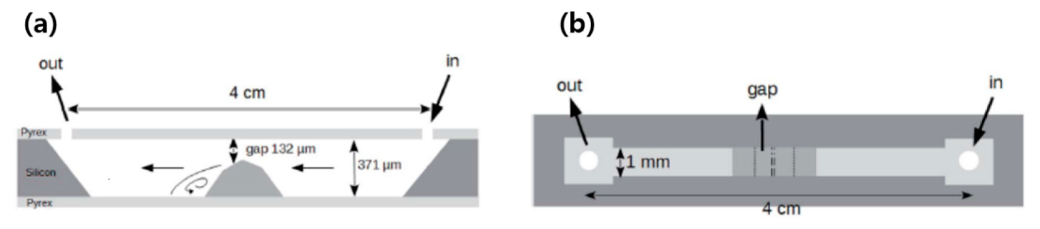
  32. Choi, C.-H.; Park, Y.-J.; Wu, X.; Kim, D.-P. Highly efficient and continuous production of few-layer black phosphorus nanosheets and quantum dots via acoustic-microfluidic process. Chem. Eng. J. 2018, 333, 336–342. [Google Scholar] [CrossRef]
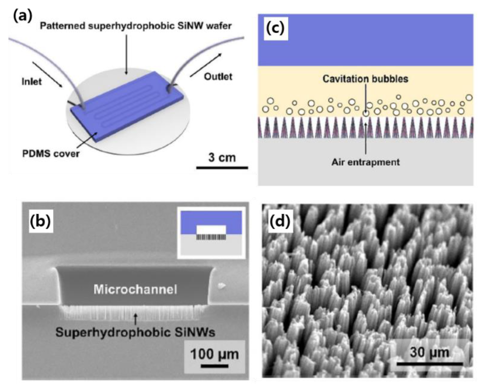
  33. Choi, C.-H.; Ko, D.-H.; Jun, H.Y.; Ryu, S.O.; Kim, D.-P. Rapid exfoliation for few-layer enriched black phosphorus dispersion via a superhydrophobic silicon-nanowire-embedded microfluidic process. Green Chem. 2020. [Google Scholar] [CrossRef]
  34. Li, H.; Li, Y.; Aljarb, A.; Shi, Y.; Li, L.-J. Epitaxial growth of two-dimensional layered transition-metal dichalcogenides: Growth mechanism, controllability, and scalability. Chem. Rev. 2017, 118, 6134–6150. [Google Scholar] [CrossRef] [PubMed]
  35. Shi, Y.; Li, H.; Li, L.-J. Recent advances in controlled synthesis of two-dimensional transition metal dichalcogenides via vapour deposition techniques. Chem. Soc. Rev. 2015, 44, 2744–2756. [Google Scholar] [CrossRef] [PubMed]
  36. Li, X.; Cai, W.; An, J.; Kim, S.; Nah, J.; Yang, D.; Piner, R.; Velamakanni, A.; Jung, I.; Tutuc, E. Large-area synthesis of high-quality and uniform graphene films on copper foils. Science 2009, 324, 1312–1314. [Google Scholar] [CrossRef] [Green Version]
  37. Lee, Y.H.; Zhang, X.Q.; Zhang, W.; Chang, M.T.; Lin, C.T.; Chang, K.D.; Yu, Y.C.; Wang, J.T.W.; Chang, C.S.; Li, L.J. Synthesis of large–area MoS2 atomic layers with chemical vapor deposition. Adv. Mat. 2012, 24, 2320–2325. [Google Scholar] [CrossRef] [Green Version]
  38. Mattevi, C.; Kim, H.; Chhowalla, M. A review of chemical vapour deposition of graphene on copper. J. Mat. Chem. 2011, 21, 3324–3334. [Google Scholar] [CrossRef]
  39. Lin, W.-H.; Brar, V.W.; Jariwala, D.; Sherrott, M.C.; Tseng, W.-S.; Wu, C.-I.; Yeh, N.-C.; Atwater, H.A. Atomic-scale structural and chemical characterization of hexagonal boron nitride layers synthesized at the wafer-scale with monolayer thickness control. Chem. Mat. 2017, 29, 4700–4707. [Google Scholar] [CrossRef] [Green Version]
  40. Son, D.; Chae, S.I.; Kim, M.; Choi, M.K.; Yang, J.; Park, K.; Kale, V.S.; Koo, J.H.; Choi, C.; Lee, M. Colloidal synthesis of uniform–sized molybdenum disulfide nanosheets for wafer–scale flexible nonvolatile memory. Adv. Mat. 2016, 28, 9326–9332. [Google Scholar] [CrossRef]
  41. Kang, J.; Sangwan, V.K.; Wood, J.D.; Hersam, M.C. Solution-based processing of monodisperse two-dimensional nanomaterials. Acc. Chem. Res. 2017, 50, 943–951. [Google Scholar] [CrossRef]
  42. Bonaccorso, F.; Bartolotta, A.; Coleman, J.N.; Backes, C. 2D–crystal–based functional inks. Adv. Mat. 2016, 28, 6136–6166. [Google Scholar] [CrossRef] [PubMed]
  43. Backes, C.; Szydłowska, B.M.; Harvey, A.; Yuan, S.; Vega-Mayoral, V.; Davies, B.R.; Zhao, P.-L.; Hanlon, D.; Santos, E.J.; Katsnelson, M.I. Production of highly monolayer enriched dispersions of liquid-exfoliated nanosheets by liquid cascade centrifugation. ACS Nano 2016, 10, 1589–1601. [Google Scholar] [CrossRef] [PubMed]
  44. Kang, J.; Wells, S.A.; Wood, J.D.; Lee, J.-H.; Liu, X.; Ryder, C.R.; Zhu, J.; Guest, J.R.; Husko, C.A.; Hersam, M.C. Stable aqueous dispersions of optically and electronically active phosphorene. Proc. Natl. Acad. Sci. USA 2016, 113, 11688–11693. [Google Scholar] [CrossRef] [PubMed] [Green Version]
  45. Gall, V.; Runde, M.; Schuchmann, H.P. Extending Applications of High-Pressure Homogenization by Using Simultaneous Emulsification and Mixing (SEM)—An Overview. Processes 2016, 4, 46. [Google Scholar] [CrossRef] [Green Version]
  46. Patrignani, F.; Lanciotti, R. Applications of High and Ultra High Pressure Homogenization for Food Safety. Front. Microbiol. 2016, 7. [Google Scholar] [CrossRef] [Green Version]
  47. Ferrari, A.; Robertson, J. Resonant Raman spectroscopy of disordered, amorphous, and diamondlike carbon. Phys. Rev. B 2001, 64, 075414. [Google Scholar] [CrossRef] [Green Version]
  48. Ferrari, A.; Rodil, S.; Robertson, J. Interpretation of infrared and Raman spectra of amorphous carbon nitrides. Phys. Rev. B 2003, 67, 155306. [Google Scholar] [CrossRef] [Green Version]
  49. Large, M.J.; Ogilvie, S.P.; Amorim Graf, A.; Lynch, P.J.; O’Mara, M.A.; Waters, T.; Jurewicz, I.; Salvage, J.P.; Dalton, A.B. Large–Scale Surfactant Exfoliation of Graphene and Conductivity–Optimized Graphite Enabling Wireless Connectivity. Adv. Mat. Technol. 2020, 2000284. [Google Scholar] [CrossRef]
  50. Nacken, T.; Damm, C.; Walter, J.; Rüger, A.; Peukert, W. Delamination of graphite in a high pressure homogenizer. RSC Adv. 2015, 5, 57328–57338. [Google Scholar] [CrossRef] [Green Version]
  51. Shang, J.; Xue, F.; Ding, E. The facile fabrication of few-layer graphene and graphite nanosheets by high pressure homogenization. Chem. Commun. 2015, 51, 15811–15814. [Google Scholar] [CrossRef]
  52. Qi, X.; Zhang, H.-B.; Xu, J.; Wu, X.; Yang, D.; Qu, J.; Yu, Z.-Z. Highly efficient high-pressure homogenization approach for scalable production of high-quality graphene sheets and sandwich-structured α-Fe2O3/graphene hybrids for high-performance lithium-ion batteries. ACS Appl. Mat. Interfaces 2017, 9, 11025–11034. [Google Scholar] [CrossRef] [PubMed]
  53. Ren, C.; Yang, B.; Wu, M.; Xu, J.; Fu, Z.; Guo, T.; Zhao, Y.; Zhu, C. Synthesis of Ag/ZnO nanorods array with enhanced photocatalytic performance. J. Hazard. Mat. 2010, 182, 123–129. [Google Scholar] [CrossRef] [PubMed]
  54. Girit, Ç.Ö.; Meyer, J.C.; Erni, R.; Rossell, M.D.; Kisielowski, C.; Yang, L.; Park, C.-H.; Crommie, M.; Cohen, M.L.; Louie, S.G. Graphene at the edge: Stability and dynamics. Science 2009, 323, 1705–1708. [Google Scholar] [CrossRef] [PubMed]
  55. Zheng, X.T.; Ananthanarayanan, A.; Luo, K.Q.; Chen, P. Glowing graphene quantum dots and carbon dots: Properties, syntheses, and biological applications. Small 2015, 11, 1620–1636. [Google Scholar] [CrossRef] [PubMed]
  56. Chong, Y.; Ma, Y.; Shen, H.; Tu, X.; Zhou, X.; Xu, J.; Dai, J.; Fan, S.; Zhang, Z. The in vitro and in vivo toxicity of graphene quantum dots. Biomaterials 2014, 35, 5041–5048. [Google Scholar] [CrossRef] [PubMed]
  57. Zhuo, S.; Shao, M.; Lee, S.-T. Upconversion and downconversion fluorescent graphene quantum dots: Ultrasonic preparation and photocatalysis. ACS Nano 2012, 6, 1059–1064. [Google Scholar] [CrossRef]
  58. Ye, R.; Xiang, C.; Lin, J.; Peng, Z.; Huang, K.; Yan, Z.; Cook, N.P.; Samuel, E.L.G.; Hwang, C.-C.; Ruan, G.; et al. Coal as an abundant source of graphene quantum dots. Nat. Commun. 2013, 4, 2943. [Google Scholar] [CrossRef]
  59. Wang, X.; Pakdel, A.; Zhang, J.; Weng, Q.; Zhai, T.; Zhi, C.; Golberg, D.; Bando, Y. Large-surface-area BN nanosheets and their utilization in polymeric composites with improved thermal and dielectric properties. Nanoscale Res. Lett. 2012, 7, 662. [Google Scholar] [CrossRef]
  60. Lin, Y.; Connell, J.W. Advances in 2D boron nitride nanostructures: Nanosheets, nanoribbons, nanomeshes, and hybrids with graphene. Nanoscale 2012, 4, 6908–6939. [Google Scholar] [CrossRef]
  61. Yuan, F.; Jiao, W.; Yang, F.; Liu, W.; Liu, J.; Xu, Z.; Wang, R. Scalable exfoliation for large-size boron nitride nanosheets by low temperature thermal expansion-assisted ultrasonic exfoliation. J. Mat. Chem. C 2017, 5, 6359–6368. [Google Scholar] [CrossRef]
  62. Seyhan, A.T.; Göncü, Y.; Durukan, O.; Akay, A.; Ay, N. Silanization of boron nitride nanosheets (BNNSs) through microfluidization and their use for producing thermally conductive and electrically insulating polymer nanocomposites. J. Solid State Chem. 2017, 249, 98–107. [Google Scholar] [CrossRef]
  63. McManus, D.; Vranic, S.; Withers, F.; Sanchez-Romaguera, V.; Macucci, M.; Yang, H.; Sorrentino, R.; Parvez, K.; Son, S.-K.; Iannaccone, G. Water-based and biocompatible 2D crystal inks for all-inkjet-printed heterostructures. Nat Nanotechnol 2017, 12, 343. [Google Scholar] [PubMed] [Green Version]
  64. Torrisi, F.; Hasan, T.; Wu, W.; Sun, Z.; Lombardo, A.; Kulmala, T.S.; Hsieh, G.-W.; Jung, S.; Bonaccorso, F.; Paul, P.J. Inkjet-printed graphene electronics. ACS Nano 2012, 6, 2992–3006. [Google Scholar] [CrossRef] [PubMed]
  65. Suslick, K.S. Sonochemistry. Science 1990, 247, 1439–1445. [Google Scholar] [CrossRef] [PubMed]
  66. Leighton, T. The Acoustic Bubble; Academic Press: Cambridge, MA, USA, 2012. [Google Scholar]
  67. Kang, J.; Wood, J.D.; Wells, S.A.; Lee, J.-H.; Liu, X.; Chen, K.-S.; Hersam, M.C. Solvent exfoliation of electronic-grade, two-dimensional black phosphorus. ACS Nano 2015, 9, 3596–3604. [Google Scholar] [CrossRef] [Green Version]
  68. Guo, Z.; Zhang, H.; Lu, S.; Wang, Z.; Tang, S.; Shao, J.; Sun, Z.; Xie, H.; Wang, H.; Yu, X.F. From black phosphorus to phosphorene: Basic solvent exfoliation, evolution of Raman scattering, and applications to ultrafast photonics. Adv. Funct. Mat. 2015, 25, 6996–7002. [Google Scholar] [CrossRef]
  69. Kou, L.Z.; Chen, C.F.; Smith, S.C. Phosphorene: Fabrication, Properties, and Applications. J. Phys. Chem. Lett. 2015, 6, 2794–2805. [Google Scholar] [CrossRef] [Green Version]
  70. Ren, X.; Zhou, J.; Qi, X.; Liu, Y.; Huang, Z.; Li, Z.; Ge, Y.; Dhanabalan, S.C.; Ponraj, J.S.; Wang, S. Few–layer black phosphorus nanosheets as electrocatalysts for highly efficient oxygen evolution reaction. Adv. Energy Mat. 2017, 7, 1700396. [Google Scholar] [CrossRef]
  71. Woomer, A.H.; Farnsworth, T.W.; Hu, J.; Wells, R.A.; Donley, C.L.; Warren, S.C. Phosphorene: Synthesis, scale-up, and quantitative optical spectroscopy. ACS Nano 2015, 9, 8869–8884. [Google Scholar] [CrossRef] [Green Version]
  72. Chen, L.; Zhou, G.; Liu, Z.; Ma, X.; Chen, J.; Zhang, Z.; Ma, X.; Li, F.; Cheng, H.M.; Ren, W. Scalable clean exfoliation of high–quality few–layer black phosphorus for a flexible lithium ion battery. Adv. Mat. 2016, 28, 510–517. [Google Scholar] [CrossRef]
  73. Liu, H.; Neal, A.T.; Zhu, Z.; Luo, Z.; Xu, X.; Tománek, D.; Ye, P.D. Phosphorene: An unexplored 2D semiconductor with a high hole mobility. ACS Nano 2014, 8, 4033–4041. [Google Scholar] [CrossRef] [PubMed] [Green Version]
  74. Bremond, N.; Arora, M.; Ohl, C.D.; Lohse, D. Controlled multibubble surface cavitation. Phys. Rev. Lett. 2006, 96, 224501. [Google Scholar] [CrossRef] [PubMed] [Green Version]
  75. Fernandez Rivas, D.; Prosperetti, A.; Zijlstra, A.G.; Lohse, D.; Gardeniers, H.J. Efficient sonochemistry through microbubbles generated with micromachined surfaces. Angew. Chem. 2010, 49, 9699–9701. [Google Scholar] [CrossRef] [Green Version]
  76. Choi, C.-H.; Ko, D.-H.; Park, B.; Choi, Y.; Choi, W.; Kim, D.-P. Air-water interfacial fluidic sonolysis in superhydrophobic silicon-nanowire-embedded system for fast water treatment. Chem. Eng. J. 2019, 358, 1594–1600. [Google Scholar] [CrossRef]
  77. Oztekin, R.; Sponza, D.T. Effect of sonication on the treatment of polycyclic aromatic hydrocarbons (PAHs) in a petrochemical industry wastewater and toxicity evaluations. Desalin. Water Treat. 2011, 26, 24–38. [Google Scholar] [CrossRef]
  78. Manariotis, I.D.; Karapanagioti, H.K.; Chrysikopoulos, C.V. Degradation of PAHs by high frequency ultrasound. Water Res. 2011, 45, 2587–2594. [Google Scholar] [CrossRef]
  79. Gielen, B.; Jordens, J.; Janssen, J.; Pfeiffer, H.; Wevers, M.; Thomassen, L.C.; Braeken, L.; Van Gerven, T. Characterization of stable and transient cavitation bubbles in a milliflow reactor using a multibubble sonoluminescence quenching technique. Ultrason. Sonochem. 2015, 25, 31–39. [Google Scholar] [CrossRef]
  80. Hatanaka, S.-I.; Mitome, H.; Yasui, K.; Hayashi, S. Multibubble sonoluminescence enhancement by fluid flow. Ultrasonics 2006, 44, e435–e438. [Google Scholar] [CrossRef]
  81. Zhou, Q.H.; Chen, Q.; Tong, Y.L.; Wang, J.L. Light-Induced Ambient Degradation of Few-Layer Black Phosphorus: Mechanism and Protection. Angew. Chem. Int. Ed. 2016, 55, 11437–11441. [Google Scholar] [CrossRef]
  82. Huang, Y.; Qiao, J.; He, K.; Bliznakov, S.; Sutter, E.; Chen, X.; Luo, D.; Meng, F.; Su, D.; Decker, J. Interaction of black phosphorus with oxygen and water. Chem. Mat. 2016, 28, 8330–8339. [Google Scholar] [CrossRef] [Green Version]
  83. Ding, X.; Li, P.; Lin, S.-C.S.; Stratton, Z.S.; Nama, N.; Guo, F.; Slotcavage, D.; Mao, X.; Shi, J.; Costanzo, F. Surface acoustic wave microfluidics. Lab Chip 2013, 13, 3626–3649. [Google Scholar] [CrossRef] [PubMed]
  84. Destgeer, G.; Sung, H.J. Recent advances in microfluidic actuation and micro-object manipulation via surface acoustic waves. Lab Chip 2015, 15, 2722–2738. [Google Scholar] [CrossRef] [PubMed]
  85. Kim, K.-J.; Pan, C.; Bansal, S.; Malhotra, R.; Kim, D.-H.; Chang, C.-H. Scalably synthesized environmentally benign, aqueous-based binary nanoparticle inks for Cu2ZnSn(S,Se)4 photovoltaic cells achieving over 9% efficiency. Sustain. Energy Fuels 2017, 1, 267–274. [Google Scholar] [CrossRef]
  86. Hwang, H.-J.; Zeng, C.; Pan, C.; Dexter, M.; Malhotra, R.; Chang, C.-H. Tuning electronic and photocatalytic properties in pulsed light synthesis of Cu2ZnSnS4 films from CuS-ZnS-SnS nanoparticles. Mat. Res. Bull. 2020, 122, 110645. [Google Scholar] [CrossRef]
Figure 1. Schematic of a microfluidization process to produce few–layer 2D nanosheets (NSs) from bulk–like 2D nanosheets.
Processes 08 01067 g001
Figure 2. (a) Thickness distribution of exfoliated graphite nanosheets (inset: SEM ((scanning electron microscope) image of exfoliated graphite proceeded for 100 cycles), I(D)/I(G) as a function of (b) Disp(G) and (c) FWHM (Full width at half maximum)(G), (d) electrical conductivity as a function annealing time and temperature, (e) optical image of the screen printing process, (f) capacitive touchpad design (29 × 29 cm) printed on paper, and (g) a line on the touchpad. Reprinted with permission from reference [16], copyright 2017, American Chemical Society.
Processes 08 01067 g002
Figure 3. (a) TEM (transmission electron microscopy) and (b) high resolution transmission electron microscope (HRTEM)image of graphene quantum dots (GQDs) produced by microfluidization (inset: FFT image), (c) size distribution of GQDs (analyzed over 200 HRTEM-imaged particles), (d) AFM (atomic force microscope) image (inset: height profiles of representative particles), (e) PL (Photoluminescence) spectra of GQDs, and (f) contour map for excitation and emission of GQDs. Reprinted with permission from reference [17], copyright 2015, American Chemical Society.
Processes 08 01067 g003
Figure 4. (a,b) TEM image of hexagonal boron nitride nanosheets (BNNSs) produced by microfluidization (arrows refer to few-layer BNNSs), (c) comparing the dispersion stability of ethanol solution containing BNNSs with and without silanization, and (d) thermal conductivity comparison of polymer nanocomposites prepared with different composition (PP and VTS–BNNS denote polymer and silanized BNNS, respectively). Reprinted with permission from reference [18,47], copyright 2012 and 2017, Elsevier.
Processes 08 01067 g004
Figure 5. (a) Schematic of wet-jet milling system (the arrows indicate the flow direction of dispersion) and (b) closed view of the processor (Disk B can be varied to 0.10, 0.20, 0.30 mm nozzle diameter upon the size of the 2D nanosheets in dispersion). Reprinted with permission from reference [22], copyright 2018, Royal Society of Chemistry.
Processes 08 01067 g005
Figure 6. (a) TEM images and lateral size distribution histogram (inset) of graphite nanosheets processed at WJM with different nozzle diameter (0.30, 0.15, and 0.10 denote the nozzle diameter 0.30, 0.15, and 0.10 mm, respectively), (b) HRTEM image of three-layer graphene, (c) HRTEM image of WJM 0.10 flake showing A–B stacking (upper inset: closed-view area of nanosheet indicated by yellow and orange circles displays hexagonal unit cell of graphite, bottom inset: FFT image), (d) AFM image of WJM 0.10 flake (inset: thickness distribution histogram), (e) TEM images and lateral size distribution histogram (inset) of MoS2, WS2, and h-BN nanosheets, (f) AFM images and thickness distribution histogram (inset) of MoS2, WS2, and h-BN nanosheets. Reprinted with permission from reference [22], copyright 2018, Royal Society of Chemistry.
Processes 08 01067 g006
Figure 7. (a) Schematic of the acoustic–microfluidic (AM) exfoliation process, (b) TEM image of few-layer black phosphorus (BP) flake, and (c) TEM and HRTEM image of BPQDs. Reprinted with permission from reference [24], copyright 2018, Elsevier.
Processes 08 01067 g007
Figure 8. (a) Time sequence displaying the nucleation and collapse of bubbles from the hydrophobic hexagonal patterned surface and (b) cavitation effects with respect to the number of nucleation sites (radical formation rate shown on the y-axis is proportional to cavitation effects). Reprinted with permission from reference [59], copyright 2006, Elsevier and from reference [60], copyright 2010, John Wiley and Sons.
Processes 08 01067 g008
Figure 9. (a) Schematic of superhydrophobic silicon nanowire SiNW microfluidic device, (b) cross-sectional view of the device, (c) conceptual illustration of cavitation bubble generation at the air-water fluidic interface, and (d) SEM image of superhydrophobic SiNW bundles. Reprinted with permission from reference [61], copyright 2019, Elsevier.
Processes 08 01067 g009
Figure 10. (a) Cavitation effects concerning flow rate and power density of sonication (emission rate in the y-axis corresponds to cavitation effects), (b) schematic of fragmentation and delamination of BP under controlled cavitation effects in the superhydrophobic SiNW microfluidic device, and (c) AFM, (HR)TEM, and size distribution histogram of few-layer BP nanosheets. Reprinted with permission from reference [25], copyright 2020, Royal Society of Chemistry.
Processes 08 01067 g010
Figure 11. (a) Schematic of a chip–scaled piezoelectric device to illustrate the process of 2D flake exfoliation, (b) magnification of the schematic that displays dispersion wicking and generation of acoustic streaming, (c) schematic illustration of the exfoliation mechanism for 2D nanosheets with piezoelectric and without piezoelectric property, (d) schematic illustration of the process for simultaneous exfoliation of 2D nanosheets and stencil printing. Reprinted with permission from reference [21], copyright 2018, John Wiley and Sons.
Processes 08 01067 g011
Figure 12. Schematic of a “lab–on–a–chip” (LOC) device: (a) profile view and (b) top view. Reprinted with permission from reference [19], copyright 2019, Royal Society of Chemistry.
Processes 08 01067 g012

