Article

Self-Adaptation of Oxygen Adsorption and Sub-Surface Junction Formation in Thin Nanometric Sheets of Metal Oxides

by
Gerhard Müller
1,* and
Giorgio Sberveglieri
2,*
1
Department of Applied Sciences and Mechatronics, Munich University of Applied Sciences, D-80335 Munich, Germany
2
Department of Information Engineering, University of Brescia, Via Branze, 38, 25123 Brescia, Italy
*
Authors to whom correspondence should be addressed.
Chemosensors 2023, 11(6), 352; https://doi.org/10.3390/chemosensors11060352
Submission received: 23 May 2023 / Revised: 12 June 2023 / Accepted: 15 June 2023 / Published: 20 June 2023

Abstract

:
Oxygen adsorption at metal oxide (MOX) surfaces and the formation of sub-surface depletion zones in thin nanometric sheets of MOX materials are theoretically investigated. It is shown that—under conditions of sufficient oxygen mobility—the bulk thermal generation of oxygen vacancy donors and the adsorption of surface oxygen ions cooperate in a self-organizing manner to form narrow sub-surface depletion zones which optimally fit into the limited spaces of MOX layers with nanometric cross sections. With this self-organization process in place, both the oxygen adsorption at free surfaces and the bulk generation of oxygen vacancy donors continuously increases as the MOX sheet thickness L is reduced, maintaining at the same time overall electro-neutrality and a state of perfect volume depletion of free carriers in bulk. This process comes to an end when MOX sheet thicknesses of L ≈ 1 nm are approached and when 3d-volumes of about 1 nm3 contain only one single double-donor and two surface oxygen ions on average. It is argued that at this limit of miniaturization, different interpretations of MOX gas sensing phenomena might be required than on larger length scales.

1. Introduction

Metal oxide (MOX) gas sensors and sensor arrays, i.e., E-Noses [1], are widely employed in the detection of gases and gas concentrations in the ambient air to aid in a multitude of safety, security, medical, automotive and industrial control scenarios [2,3,4,5,6,7,8,9,10,11,12,13]. All of these applications have been enabled by making progress along the three main directions of research, namely by striving for higher sensitivity, selectivity and stability [14].
As is well known, MOX gas sensors respond to a multitude of gases with high sensitivity; however, these also suffer from poor selectivity and sensor drift. While selectivity problems could be dealt with by forming arrays of sensors with different cross-sensitivity profiles, much less progress has been made in the capability of detecting, compensating and mitigating the effects of sensor drift in MOX gas sensor arrays. With properly chosen sensors and sensor operation conditions, arrays of cross-sensitive sensors can be constructed to detect odor patterns that are characteristic of certain application scenarios and to distinguish these from interferent patterns that might turn up in these same scenarios. Problems with selectivity can arise in the case individual sensors within an array drift over the course of time at different speeds and in different directions. In such an event, odor recognition capabilities of E-Nose devices could deteriorate and eventually lead to a misfunctioning of such devices. Making progress in the direction of higher device stability is therefore essential for arriving at higher-performance E-Nose devices.
In view of this situation, we have decided to identify physical mechanisms which underly the processes of gas sensor drift and to eventually arrive at more stable and higher-performance gas sensors. Working in this direction, we have shown in a recent paper [15] that experimentally observed long-term drifts in the baseline conductance of high-temperature deposited SnO2 nanowire gas sensors can be understood in terms of an innovative equilibrating donor approach. The key idea in this approach is that the electronic properties of such high-temperature-deposited materials are not determined by metal impurities whose concentrations are permanently fixed during materials preparation but rather by oxygen-vacancy donors thermally generated during high-temperature deposition and quenched in as the temperature of the nanowires had been lowered into the range of normally employed sensor operation temperatures. With the quenched-in oxygen vacancy donors being key elements of the thermal lattice disorder, the concentration of such donor defects and their electrical charge states can adapt to the specific sensor operation conditions even after sensor preparation had taken place. The key enabling effect in such equilibration processes is that the formation energy of positively charged vacancy donor defects is Fermi-energy-dependent, which establishes a strong link between the structural and electronic degrees of freedom inside the MOX materials. With this link in place, the baseline electronic conduction of MOX sensor materials was shown to be continually driven towards lower levels as quenched-in non-equilibrium oxygen vacancy donors slowly anneal out and approach their sensor-operation-specific equilibrium concentrations.
Whereas in our previous paper [15], our focus had been on the bulk property of long-term drift of the sensor baseline conductance in MOX materials, the focus in our present paper is on the surface and sub-surface effects of oxygen adsorption and sub-surface junction formation. Dealing with thin sheets of MOX materials with nanometric cross sections and infinitely extended surfaces, at which oxygen adsorption processes can take place, we study the effects of equilibration on the bulk donor and oxygen adsorbate concentrations as the cross-sectional dimensions L of the MOX sensor sheets are scaled down to increasingly lower values. Following this road towards lower L , we show that—under conditions of sufficient internal oxygen mobility—the coupled processes of bulk thermal generation of oxygen vacancies and the formation of oxygen ion adsorbates cooperate in such a way as to fit the ensuing sub-surface depletion zones into the increasingly narrower spaces of the MOX sensor sheets. In this way, a state of perfect volume depletion [16,17,18] from mobile charge carriers is maintained down to the lowest levels of L . This process of downscaling comes to a natural end as cross sections of L 1   nm are approached, where a cube of 1   nm side length would contain only one single oxygen-vacancy donor and two associated surface oxygen ions on average. At and around this level of miniaturization, the concept of homogeneously spread-out donor charges and ensuing electrical field and potential distributions arising from Poisson’s equation solutions becomes overstrained, possibly calling for new explanations of the MOX gas sensitivity at the single- nm scale that go beyond the familiar double-Schottky-barrier model (DSBM) approaches, widely discussed in the literature [19,20,21,22,23].
In presenting our arguments, the paper is organized as follows: in Section 2, the close coupling of bulk thermal donor generation and the formation of surface oxygen ion adsorbates is explained. Section 3 presents arguments that the rate of generation of positively charged oxygen vacancy donors in the bulk not only depends on the momentary values of the sensor operation temperature T but also on the value of the band bending potential φ ( x , T ) at the sites of vacancy formation. With φ ( x , T ) controlling the rate of generation of oxygen vacancy donors and the local densities of oxygen vacancy donors determining the degree of local band bending, an element of self-organization emerges that controls the formation of sub-surface depletion zones. This proposition of a self-organizing formation of sub-surface depletion zones inside MOX nanostructures is tested in Section 4, where thin and infinitely extended sheets of MOX materials are analyzed by integrating Poisson equations with band-bending-dependent local donor charge densities. In this way, the internally arising electrical field and electron potential distributions are derived. The results show that at typical sensor operation temperatures, sub-surface space charge zones with approximately triangular potential profiles will develop, which optimally fit into the narrow spaces inside the MOX nanostructures. The limits to this kind of geometrical downscaling are discussed in Section 5. There, a brief look at nanogranular materials [24,25,26,27,28,29,30,31,32,33] and the issue of a possibly minimum gas-sensitive grain size in MOX materials [34,35,36] is undertaken. Section 6 finally summarizes our results and points out opportunities for further research.

2. Coupling of Bulk and Surface Processes

In metal oxides, the key elements of lattice disorder are oxygen vacancies V O which are formed by thermally exciting oxygen atoms out of oxygen lattice sites O O [37,38,39,40,41,42,43,44,45]. The emitted oxygen atoms, on the other hand, are injected into the nearby interstitial O i lattice sites, thus turning them into mobile species:
O O   V O 0 + O i .
As the initial O O lattice sites had been occupied by O 2 ions, the empty vacancy sites form double donors, which still leave two electrons to be emitted out of the vacancies into empty conduction band states. In this way, mobile electrons and two kinds of positively charged vacancies can be formed:
V O 0   V O + + e ,   and
V O +   V O 2 + + e .
In Figure 1a, a V O 2 + donor vacancy is thermally generated inside a thin sheet of MOX material, leaving behind in the bulk an O i interstitial and two mobile electrons. As in this configuration, the negative charge of the two electrons is compensated by the positive charge of the immobile V O 2 + ion, a configuration with bulk electrical conductivity and zero gas sensitivity has emerged.
In Figure 1b, the two electrons and the interstitial oxygen atom have migrated against the attractive force of the central V O 2 + ion towards both nearest-neighbor surfaces, thus forming surface oxygen ion adsorbates O a d s on both surfaces and creating sub-surface electrical fields. As shown on the left-hand side of Figure 1b, an additional O -atom had to be captured from the air ambient to achieve full oxidation on both surfaces. While the internal electrical fields tend to re-establish the initial configuration shown in Figure 1a, it has to be kept in mind that the state of oxidized surfaces shown in Figure 1b is stabilized by the release of adsorption energy of about 1   eV per ion [46,47,48] as the O a d s adsorbates are being formed. Due to the transfer of the two electrons to surfaces and their immobilization at oxygen ion adsorbates, the configuration in Figure 1b is electrically non-conducting but potentially gas sensitive as reducing gas species in the air ambient can interact with the surface oxygen ions, thus releasing an electron which is mobile inside the bulk [40,44,45]:
C O + O a d s C O 2 + e .
As with the exception of Equation (4), all reactions are reversible; it becomes evident that—given close surfaces and sufficient oxygen mobility—MOX materials are able to alternate between internally conductive but non-gas sensitive and non-conducting but gas sensitive states. Further considering that upon cooling to T 0 , all vacancies inside the bulk will anneal out, re-forming a fully coordinated MOX lattice with all metal atoms on M e M e and all O -atoms on O O sites [15], it is clear that any gas sensitivity will vanish in this limit as well. In practice, however, such stable but insensitive states will never be formed as oxygen diffusion rates D ( T ) are exponentially activated and thus also tend to zero in the limit T 0 [49,50,51,52]:
D ( T ) = D 0   e x p [ E a k B T ] .
In this latter equation E a stands for the activation energy of oxygen diffusion, k B for Boltzmann’s constant and T for the sensor operation temperature; D 0 , finally, is the diffusion constant as extrapolated towards infinite temperature. Considering a thin sheet of MOX material of thickness L , surface diffusion across a distance of L / 2 at a temperature T e q will take characteristic times:
τ e q ( T e q ) = L 2 4   D 0 e x p [ E a k B T e q ] ,
which will exponentially rise upon cooling to increasingly lower temperatures. We have already shown in our previous paper [15] that such time constants are very short during high-temperature preparation of nanometric structures but very long in the order of months or even years in the range of normally employed sensor operation temperatures. For the purpose of illustration, some of those time constants τ e q ( T e q ) have been quantitatively evaluated and listed in Table 1.
In the following, we focus on cases of complete equilibration of all electronic and structural degrees of freedom. In order to indicate this, we consistently denote equilibration temperatures by T e q to distinguish these from directly accessible sensor operation temperatures T and situations in which only partial equilibria had been attained where the available electronic degrees of freedom had equilibrated towards quenched-in and slowly relaxing structural non-equilibrium states.

3. Coupling between Electronic and Structural Degrees of Freedom

In the above section, we have shown that the internal processes of vacancy formation in the bulk and oxygen diffusion toward surfaces can create activated configurations with adsorbed surface oxygen ions that are gas sensitive. In this section, we provide evidence that the electrical fields generated by such oxygen ion adsorbates also react back onto the bulk, thus modifying the ease with which donor vacancies and their different charge states can be created there.
Upon starting our considerations, we graphically illustrate in Figure 2a the ability of oxygen vacancies in the MOX bulk to function as double donors of electrons. With two electrons being initially bound to neutral oxygen vacancies, such vacancies are free to transfer their electrons either to unoccupied conduction- or empty valence-band states. Considering large ensembles of transferred electrons, such transfers statistically correspond to simple downward transitions towards fictive and unoccupied electron states positioned at the equilibrium Fermi energy E F ( T ) . As indicated in Figure 2b, the extra energy added to the reservoir of MOX lattice vibrations enables electrons to be re-excited to the conduction band edge from where they can contribute to the electronic conduction inside the MOX material.
In the analysis of MOX sensor properties, it is often implicitly assumed that the total density of oxygen vacancy donors is permanently fixed during materials preparation and that thereafter only redistribution processes of electrons among all available electron states can take place. As this scenario fails to account for the post-deposition phenomena of baseline conductivity drift and ensuing changes in the reducing gas response, we have proposed in our previous publication [15] that—with oxygen vacancy donors being key elements of the thermal lattice disorder in MOX materials—the densities of the donor vacancies and their different charge states can adapt to changes in the sensor operation temperature even after sensor preparation had taken place. The key idea in this proposal was that the energy releases in the downward electronic transitions in Figure 2b can be directly re-invested in alleviating the formation of oxygen vacancies, thus turning them directly into singly and doubly ionized positive oxygen vacancy donors. Due to the electronic energy gains that are immediately realized during the vacancy formation process, the formation energies of positively charged vacancies are lowered, with the result that the densities of charged oxygen vacancy donors tend to significantly outnumber the densities of neutral vacancies:
N V O 0 ( T ) = N O e x p [ E V O 2   k B T ] ,
N V O + ( T ) = 2 N V O 0 ( T ) e x p [ E V O 1 E F ( T ) k B T ] ,
N V O 2 + ( T ) = N V O 0 ( T )   e x p [ E V O 1 E F ( T ) k B T ] e x p [ E V O 2 E F ( T ) k B T ] .
In these latter equations E V O stands for the formation energy of neutral donor vacancies, which in the case of SnO2 is about 4   eV [53] and E V O 1 E F ( T ) and E V O 2 E F ( T ) for the electronic energy gains indicated in Figure 2b. The factor of two in Equation (8), on the other hand, takes care of the spin degeneracy of singly ionized oxygen vacancy donors [15].
With the charged donor vacancies taking part in the electronic redistribution processes inside the MOX materials, the condition for overall charge-neutrality at each temperature T reads [15,42,43]:
n ( T ) = N V O + ( T ) + N V O 2 + ( T ) + p ( T ) .
There n ( T ) and p ( T ) are the electron and hole densities in the conduction and valence band states and N V O + ( T ) and N V O 2 + ( T ) the volume densities of positively charged donor vacancies as defined in Equations (8) and (9). With the simplifications p ( T ) 0 and N V O + ( T ) N V O 2 + ( T ) the position of the common Fermi energy E F ( T ) relative to the conduction band edge E C emerges as [15]:
E C E F ( T ) = 1 3 { E V O e f f 2 k B   T   l n [ N O N C ( T ) ] } .
There, N C ( T ) is the effective conduction band density of states [42,43] and E V O e f f the effective donor vacancy formation energy [15]
E V O e f f = E V 0 + 2 ( E C E O 1 ) + 2 ( E C E O 2 ) .
With E F ( T ) being fixed, the concentrations of mobile electrons and of two-fold positively charged oxygen vacancy donors can be calculated that would turn up in a piece of MOX material that is operated at a constant temperature T under flat-band conditions and for a time long enough so that all redistribution processes of electrons and oxygen interstitials have come to an end. Up to this point, our arguments have been repeating all those ideas already introduced in our previous paper dealing with the bulk effect of sensor baseline conductivity drift [15].
In order to get insight into situations in which flat-band conditions no longer apply, consider Figure 3, where a n-p junction scenario with an abrupt interface has been envisaged. While on the left-hand side of Figure 3, the MOX material is n-type doped by the naturally occurring oxygen vacancy donors, the right-hand side had additionally been doped by a large number of compensating deep acceptor impurities during preparation. As shown in our previous paper [15], these latter impurities allow the Fermi energy to move somewhat deeper into the band gap but not to the extent that a true conversion to p-type conduction can be attained. Upon bringing both sides into contact, the higher electron densities on the left-hand side will tend to spread over onto the less electron-conducing right-hand side, thus producing a potential step several tenths of an electron volt high. Whereas in a fixed donor scenario, parabolic potential profiles with different slopes are expected to arise at the two sides of the interface, the situation changes once an equilibrating donor scenario is envisaged. In this latter case, vacancy donors forming on the right-hand side will benefit from larger electronic energy gains than those on the left-hand side, thus causing the junction to become more abrupt and the potential profile at the interface to become non-parabolic. Returning to Figure 2 and Equations (9) and (10) and considering that the donor binding energies E O 1 and E O 2 are small compared with the energy gains E V O 1 E F ( T ) and E V O 2 E F ( T ) the energy gains in Equations (8) and (9) can be approximated by the magnitude of the local band bending potential φ ( x ) at each position x . In this way, Equations (8) and (9) simplify into [15]
N V O + ( x , T ) = 2 N V O 0 ( T ) e x p [ q φ ( x , T ) k B T ] ,   and
N V O 2 + ( x , T ) = N V O 0 ( T ) e x p [ 2 q φ ( x ,     T ) k B T ] .
With the help of such band bending-dependent charge densities, the ensuing changes in potential profiles and internal electrical field distributions can be obtained by solving Poisson´s equation with space charge densities which by themselves depend on those band bending potentials which are induced by the negative ion adsorbate layers on both surfaces.

4. Junction Formation and Sub-Surface Vacancy Re-Arrangement in the Equilibration Scenario

4.1. Potential and Electrical Field Distributions across MOX Sensor Sheets

In this section, we investigate some of those consequences that arise out of Equations (13) and (14). As a specific test, we consider oxygen adsorption on a thin planar sheet of MOX material with infinite extensions in both planar directions and a very thin cross-section with nanometric dimensions L   in the cross-sectional x -direction. Being very thin and operated at relatively high temperatures, any positively charged vacancies generated at and around the center plane at x = 0 will produce reaction products that can easily and rapidly reach either of the two surfaces, thus forming oxygen ion adsorbates. As already discussed in Section 3, such adsorbates, in turn, generate electrical fields inside the MOX layer, which, according to Equations (13) and (14), influence the build-up of positive space charge within this layer.
In order to arrive at quantitative results, Poisson´s equation has to be solved with the positive space charge inside the MOX layer depending on the local degree of band bending φ ( x , T e q ) at each particular cross-sectional coordinate x :
d 2 d x 2 φ ( x , T e q ) = q ε ε 0 N V O 2 + ( T e q )   e x p [ 2 q φ ( x , T e q ) k B T ] .
In Equation (15), we have made the simplifying assumption that due to the factor of two in the exponential term, doubly charged oxygen vacancy donors will make the dominant contribution to the positive space charge inside the MOX layer. Further, considering that valid solutions need to be symmetrical with regard to the central plane at x = 0 , the general solution to Equation (15) reads:
φ ( x , T e q , C 1 ) = [ k B T e q 2 q ] l n { C 1 κ   k B   T e q N V O + + ( T e q ) cos h [ x   q   C 1 k B T e q ] } .
In this equation κ = q ε ε 0 with q standing for the elementary charge and ε 0 and ε for the absolute values and relative values of the dielectric constant. C 1 , finally, is a free parameter that allows the solutions φ ( x , T e q ) to comply with the boundary conditions on φ at both surfaces.
With the parameter values of C 1 still leaving undetermined, solutions for the electronic potential energy distribution
E e l ( x , T e q , C 1 ) = q [ φ ( 0 , T e q , C 1 ) φ ( x , T e q , C 1 ) ] ,
the internal electrical fields
E ( x , T e q , C 1 ) = d d x φ ( x , T e q , C 1 ) = C 1 q t a n h ( x   q   C 1 k B T e q ) ,
and the volume densities of positive N V O 2 + space charges inside the bulk layer can be obtained:
N V O 2 + ( x , T e q , C 1 ) = ( ε ε 0 q )   d 2 d x 2 φ ( x , T e q , C 1 ) .
In Figure 4, specific solutions for the above four quantities are shown, assuming that the MOX layer thickness is L = 10   nm . Boundary conditions at all temperatures had been φ ( x S ) = 0 at both surfaces, i.e., at x S = ± L / 2 . This assumption derives from the fact that the negatively charged surface oxygen ion adsorbate layers have essentially zero thickness as compared to the bulk MOX layer. Any potential drops developing across these adsorbate layers can therefore be neglected in comparison with the much larger potential drops that build up across the MOX layer itself.
Figure 4a shows the form of the band bending profile as derived from Equation (16). From room temperature up to 700 K, which is close to the upper bound of MOX gas sensor operation temperatures, the function φ ( x , T e q ) takes an almost triangular shape with a maximum at the position of the center plane at x = 0 . Also shown in Figure 4a is a dashed line of nearly parabolic shape that occurs when φ ( x , T e q ) is evaluated at the maximum temperature at which valid solutions to Equation (15) could still be obtained. Figure 4b shows that—in agreement with Equation (16)—the induced positive donor space charge density N V O 2 + ( x , T e q ) goes through a pronounced maximum at the position of the center plane, falling off towards very small values at both surfaces. Figure 4c, in turn, shows the electrical field distributions E ( x , T e q ) that are induced by the cooperation of the negative adsorbate layers on both surfaces and the induced positive space charge within the MOX bulk. The high and almost constant electrical field distributions with a switch in directions at and around the center plane derive from the fact that the negative adsorbate charges on the left-hand surface produce a high negative field inside the left-hand portion of the MOX bulk, which upon approaching the center plane, becomes increasingly shielded and finally overcompensated by the positive bulk space charge distributions at and around the center plane (Figure 4b), thus inducing a field reversal and a high positive electrical field on the right-hand side, which is finally shielded and compensated upon entering the negative adsorbate layer on the right-hand surface. As both fields on the left- and right-hand sides tend to attract mobile electrons towards the center plane, the electron potential energy increases towards both surfaces (Figure 4d). The pronounced linearity of these potential energy curves is a direct consequence of the almost constant electrical field profiles in Figure 4c.
Whereas the results in Figure 4 specifically relate to MOX sensor sheets with a cross-sectional thickness of L = 10   nm , similar triangular-shaped electron potential profiles were obtained over a much wider range of thicknesses. Figure 5 shows some exemplary solutions which had been obtained by varying L all throughout the range 100   nm   L   1   nm . As a representative value of the equilibration temperature, T e q = 600   K had been chosen, which falls well within the range of conventionally applied MOX sensor operation temperatures. Figure 5a shows that independent of the MOX layer thicknesses, the same kind of triangular potential energy distributions are recovered as long as the actual x -coordinates are replaced by the reduced coordinates x r e d ( L ) = x / L . What remains after rescaling is that the height of the surface electron barriers shows moderate variations with equilibration temperature and MOX sheet thickness. Figure 5b shows the corresponding electrical field distributions. This latter data set shows that, in contrast to the surface potential barrier heights, the surface electrical field strengths E S = E ( T e q , L ) exhibit huge dependencies on L . While moderate electrical field strengths abound in relatively thick layers with L 100   nm , very high electrical fields ranging up to about 10 7   V / cm are predicted to develop in very thin layers with L 1   nm only. Considering that such calculated field strengths are well beyond the breakdown electrical field in SnO2 [54] and also beyond accepted limits enshrined in the Weisz limitation [55,56], it appears that the physical assumptions underlying the validity of Equation (15) are becoming increasingly overstrained when cross-sectional dimensions in the range of single nanometers are approached. This problem will be further discussed in Section 5.

4.2. Supporting Electrical Charge Distributions

Seeing that the thickness scaling of the triangular potential energy distributions above is enabled by huge increases in the internal electrical field strengths as MOX sensor sheet thicknesses are reduced, a closer look at the field-generating space charge distributions is suggested. Starting with the negative surface adsorbate layers on both sides, the areal densities of surface oxygen ions N O a d s ( T e q , L ) need to comply with Poisson’s equation and the surface electrical field strengths E S ( T e q , L ) acting at both surfaces. With the solutions for E S ( T e q , L ) obtained from Equation (17) and the values of C 1 ( T e q , L )   associated with the individual values of T e q   and L , the surface space charge densities then derive from:
N O a d s ( T e q , L ) = κ   E S ( T e q , L ) .
The areal densities of positive charges in the MOX bulk, on the other hand, easily derive from integration over the N V O 2 + ( x , T e q , L ) profiles deriving from Equation (19) and exemplarily shown in Figure 5b:
S N V O 2 + ( T e q , L ) = L 2 L 2 N V O 2 + ( x , T e q , L ) d x .
The variation of both kinds of space charge densities with MOX sheet thickness L and equilibration temperature T e q is shown in Figure 6a, revealing that both charge densities scale up with decreasing MOX sheet thickness, following at the same time a parallel trend with L
S N V O 2 + ( T e q , L )   ~   N V O 2 + ( T e q , L )   ~ L 2.5 ,
and maintaining a constant distance from each other, satisfying
2   N O a d s ( T e q , L ) = S N V O 2 + ( T e q , L ) .
This latter proportionality proves that overall charge neutrality is maintained all throughout the entire range of MOX sheet thicknesses.
Figure 6b, on the other hand, shows how the two kinds of space charge densities vary with equilibration temperature. While the dashed lines illustrate the initial state of bulk generation of oxygen vacancy donors ( V O 2 + ) and associated reaction products ( 2 e + O i ) (see Figure 1a), the full lines with symbols show the state after the V O 2 + donors and associated electrons and oxygen interstitials had become separated by diffusion to the next-nearest surfaces (see Figure 1b). The key observation here is that due to the backreaction of the negative ion adsorbates on the bulk through Equation 14, equal and largely enhanced positive and negative ion densities are induced inside the MOX nanosheets, with the largest enhancements taking place inside the thinnest MOX sheets. A second striking observation is that these enhancements are almost independent of the value of the equilibration temperature, which shows that the self-organizing state of perfect volume depletion is surprisingly stable and almost immune with regard to the deleterious effects of long-term sensor drift. Fully equilibrated nanosheets, therefore, should be unlikely to respond with drift effects in case sensor operation temperatures are changed in the course of device operation, as for instance, in non-stationary schemes of sensor operation [57,58]. This is an important difference with regard to much thicker and only partially depleted MOX sensor sheets where flat-band regions are susceptible to the effects of baseline conductance drift [15].
A downside of the results presented in Figure 6 is that in the limit of very small cross-sectional dimensions of the order of L 1   nm , very high adsorbate densities in the order of 10 14   cm 2 are predicted. As such areal charge densities imply surface electrical fields in the order of 10 7 V cm , the same concerns as those already raised in Section 4.1 above apply: such calculated adsorbate densities exceed the breakdown electrical field in SnO2 [54] and also the limits enshrined in the Weisz limitation [55,56]. As a consequence, the same considerations as those raised at the end of Section 4.1 apply, namely that solutions to Equation (15) can be mathematically scaled down to extremely low cross-sections but that the physical assumptions underlying Equation (15) may become increasingly overstrained as cross-sections L in the range of single nanometers are approached.

5. Limits to Geometrical Downscaling

In this section, we address possible physical reasons that limit the downscaling of solutions of Equation (15) towards increasingly smaller dimensions. What we should also like to do is making a digression towards nanogranular MOX materials with monolayer morphologies. In this way, we should like to contribute to the discussion of grain size effects and claims that there might be a lower limit of grain size beyond which the gas sensitivity of MOX materials does vanish [34,35,36].
Starting point of our considerations is the inset in Figure 7, where we have sketched a thin monocrystalline layer of MOX material with a thickness L . Subdividing the MOX sheet into squares with lateral side lengths L , a mental step can be taken in which the monocrystal layer is broken up into an array of weakly interlinked nanocrystals. Building on the results shown in Figure 6a, the numbers Z V O 2 + ( L ) of oxygen vacancy donors can be calculated that would fit into small crystals of size V ( L ) = L 3 . Turning to the data in Figure 7, it can be seen that crystals with side lengths in the order of 100   nm would contain roughly 100 ± 10 oxygen vacancy donors on average, while ones with side lengths of 1   nm would contain only 1 ± 1 donors on average. Considering the fact that oxygen vacancy donors and oxygen ion adsorbates can bind only multiples of the elementary charge q = 1.602 × 10 19   As , it becomes evident that at the size level of 1   nm and below, the effects of granularity of electronic charge become dominant. In the following, we call this limit the granularity limit. As argued below, some interesting consequences may arise regarding the understanding of gas sensitivity phenomena when the granularity limit of MOX nanostructures is approached.
At length scales far above the granularity limit, donor numbers per grain are relatively large and associated statistical spreads are relatively small. In this limit, the concept of homogeneously spread-out donor charge densities does make sense, and Poisson equation approaches can be used to draw up images of electrical field and electron potential energy distributions throughout each grain and across grain boundaries. Electrons generated in a reducing gas-solid interaction and traveling across several of such grain boundaries need to absorb thermal energy from the MOX grains to surmount the individual potential barriers on their way, thus leading to a thermally activated electron mobility
μ e ( T )   ~   e x p [ E b k B T ]
where E b represents the average barrier height along the transport path and k B T the mean thermal energy at the sensor operation temperature T . Such a kind of transport is depicted in Figure 8, assuming that the grain-internal potential barriers have a triangular shape and surface barrier heights in the order of tenths of electron volts, as illustrated in Figure 4d. Within this point of view, our equilibration approach largely reproduces the widely accepted DSBM pictures of the MOX gas response in nanocrystalline materials [19,20,21,22,23]. The present equilibration approach, however, does represent a step beyond the present state of the art in that it can satisfactorily explain the occurrence of volume depletion of free carriers across wide ranges of MOX sheet thicknesses and/or grain diameters and also the surprising long-term stability of such volume-depleted structures.
Things change, however, when grain sizes approach the granularity limit defined above. In this case, the statistical spread in the average number of donors per grain increases towards the average numbers themselves and even beyond as grain sizes are reduced below the granularity limit. In such a situation, crystalline structures emerge where single crystals contain one or two donors while others will not contain any donors at all. In this case, it becomes evident that the concept of homogeneously spread-out donor charge densities will lose meaning, and Poisson equation approaches aimed at arriving at smoothly varying electrical field and electron potential energy distributions across grains and grain boundaries will become increasingly more questionable. Such concerns clearly apply to the conventional DSBM approaches in the published literature [19,20,21,22,23] as well as to the equilibration approach presented in this paper.
Trying to arrive at an electron theory for the transport in nanocrystalline MOX materials, Zaretskiy et al. [34,35,36] proposed that electronic transport processes inside increasingly fine-grained MOX materials would be more appropriately described in terms of discrete electron hops rather than in terms of classical band transport theory. Hopping transport has first been intensively investigated in the field of amorphous semiconductors [59,60,61], where hopping rates between adjacent localized electron sites were found to be
ν i , j ( T )   ~ ν p h   e x p [ E i , j k B T ] e x p [ 2 R i , j α ] .
in this equation ν p h   is a typical phonon frequency, E i , j and R i , j stand for energy differences and spatial separations between adjacent states and α for the localization length of the involved states. More recently, similar kinds of transport have been observed in various kinds of nanocrystalline materials, including MOX ones [62,63,64]. It, therefore, appears plausible that in such materials, the grain-boundary modulated band transport proposed in the various DSBM approaches can be replaced by hopping transport approaches when grain sizes in the range of the granularity limit or below are approached.
Returning to Zaretskiy’s electron theory, a particularly interesting proposal was that gas sensitivity in MOX materials should vanish when hopping conduction becomes dominant and when average grain sizes are decreased below a critical value a < a C R . Estimates of a C R were estimated to be in the range of a few nanometers. Following their arguments, it is suggested that the equilibration approach introduced in our previous paper [15] and extended to the junction and sub-surface situations in this paper has pushed the limit of gas sensitivity loss from several nanometers down into the 1   nm range.
Experimental observations pointing in such a direction were recently published by Prof. Jianqiao’s group working on SnO2-based quantum dot materials [32,33]. These researchers observed a reduction in the gas sensitivity at grain sizes in the range of several nm and a complete loss at grain sizes of about 1   nm , i.e., at length scales consistent with the granularity limit defined in Figure 7 above. Interestingly also, Density Functional Theory (DFT) calculations of this same group predicted the appearance of a considerable density of localized bandgap states when grain sizes were reduced into this same range. As their films had been prepared using a hydrothermal method and low-temperature annealing only, it is, however, not yet clear whether these films had progressed to a state of complete equilibration of all structural and electronic degrees of freedom as discussed in this paper.
Returning to Zaretskiy’s proposal of variable range hopping in tiny MOX crystals, we propose that the loss of continuous percolation paths in nanogranular MOX sensing materials may cause a loss of gas sensitivity at the single nanometer scale. Aiming at a resolution of the limiting grain-size issue, we show in Figure 9 two examples of gas sensing interactions in a fine-grained MOX material with grain sizes in the range of the granularity limit. Whereas in the first case (Figure 9a), all grains had been assumed to be equal, and each grain containing one single donor, the second case considers a situation in which one of those grains—due to the effects of statistical scatter—does not contain any donor at all. Whereas in the first case, hopping transport through adjacent donor sites successfully connects the gas-solid interaction and electrode collection sites, no continuous conduction path is formed in the second case as neighboring hopping sites are separated by distances R i , j significantly longer than the electron localization lengths of the nearest-neighbor donor sites. In this kind of interpretation, a decrease in the MOX gas response at grain sizes a < a C R would arise from increasingly smaller numbers of electron percolation paths that successfully connect gas-solid interaction and electrode collection sites.

6. Summary and Conclusions

In this paper, we have studied the processes of oxygen adsorption and subsurface junction formation in thin sheets of MOX materials with nanometric cross-sections. The innovative aspect of our work has been that the recently introduced equilibration approach, which had successfully proven to explain the bulk phenomenon of baseline conductance drift in MOX gas sensors, has now been extended to analyze surface and sub-surface related phenomena in MOX gas sensors. Along this road, a number of innovative results have been obtained, which are briefly summarized below:
  • When 2d-sheets of MOX materials with nanometric cross-sections are exposed to ambient air, sub-surface depletion zones with triangular potential profiles develop below both surfaces in a state of complete equilibration which fully depletes the MOX bulk from mobile charge carriers.
  • Downscaling of the cross-sectional thickness L towards lower values enhances the adsorption of negative ion adsorbates at both surfaces, increasing at the same time the positive donor densities inside the materials to maintain overall charge neutrality. In this way, the sub-surface depletion zones shrink in a self-adaptive manner into MOX sensor sheets with increasingly lower cross-sections.
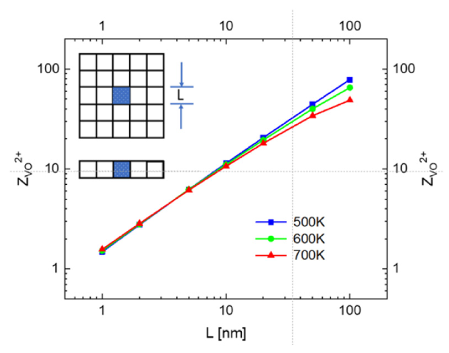
  • The shapes of equilibrated adsorbate-ion and vacancy donor distributions in fully depleted MOX sensor sheets are almost independent of the absolute value of their thermalization temperatures. Fully equilibrated MOX nanostructures should therefore reveal a promising resilience towards sensor drift when sensor operation temperatures are changed and/or methods of non-stationary sensor operation are employed [57,58].
  • The process of geometrical downscaling of MOX sensor sheets comes to a natural end when sheet thicknesses on the order of L 1   nm are approached. At that length scale, a 3d volume of 1   nm 3 would contain only one single, double donor in its bulk and one single oxygen ion adsorbate at each outer surface. With these sub-volumes only containing 2   electrons, on average, the electron granularity level is reached.
  • It is proposed that at and around the electron granularity level, the concept of homogeneously dispersed donor charge densities breaks down and that electrical field and electron potential energy profiles can no longer be determined by the conventional Poisson equation approach. At length scales smaller than the electron granularity level, electronic transport processes are likely better described in terms of discrete electron hops rather than by the conventional DSBM approaches.
  • The proposal of electron hopping in MOX materials within very small grains at present needs to be treated as a theoretical concept that can potentially explain the disappearance of gas sensitivity in the limit of extremely small grains. In order to establish this effect and its explanation as common consolidated knowledge, more experimental and theoretical work needs to be done in independent laboratories.

Author Contributions

Conceptualization, G.M. and G.S.; methodology, G.M.; software, G.M.; writing—original draft preparation, G.M.; writing—review and editing, G.S. All authors have read and agreed to the published version of the manuscript.

Funding

This work has not received external funding.

Institutional Review Board Statement

Not applicable.

Informed Consent Statement

Not applicaple.

Data Availability Statement

Not applicable.

Conflicts of Interest

The authors declare no conflict of interest.

References

  1. Gardner, J.W.; Bartlett, P.N. Electronic Noses: Principles and Application; Oxford University Press: Oxford, UK, 1999; ISBN 0-19-855955-0. [Google Scholar]
  2. Jaeschke, C.; Gonzalez, O.; Padilla, M.; Richardson, K.; Glöckler, J.; Mitrovics, J.; Mizaikoff, B. A Novel Modular System for Breath Analysis Using Temperature Modulated MOX Sensors. Multidiscip. Digit. Publ. Inst. Proc. 2019, 14, 49. [Google Scholar] [CrossRef] [Green Version]
  3. Danesh, E.; Dudeney, R.; Tsang, J.-H.; Blackman, C.; Covington, J.; Smith, P.; Saffell, J. A Multi-MOx Sensor Approach to Measure Oxidizing and Reducing Gases. Multidiscip. Digit. Publ. Inst. Proc. 2019, 14, 50. [Google Scholar] [CrossRef] [Green Version]
  4. Shaposhnik, A.; Moskalev, P.; Vasiliev, A. Selective Detection of Hydrogen and Hydrogen Containing Gases with Metal Oxide Gas Sensor Operating in Non-Stationary Thermal Regime. Multidiscip. Digit. Publ. Inst. Proc. 2019, 14, 2. [Google Scholar] [CrossRef] [Green Version]
  5. Byun, H.G.; Yu, J.B.; Kang, C.Y.; Jang, B.K.; Lee, H.R. Comparative Analysis between Blood Test and Breath Analysis Using Sensors Array for Diabetic Patients. Multidiscip. Digit. Publ. Inst. Proc. 2019, 14, 22. [Google Scholar] [CrossRef] [Green Version]
  6. Astolfi, M.; Zonta, G.; Landini, N.; Gherardi, S.; Rispoli, G.; Anania, G.; Benedusi, M.; Guidi, V.; Palmonari, C.; Secchiero, P.; et al. Chemoresistive Nanostructured Sensors for Tumor Pre-Screening. Multidiscip. Digit. Publ. Inst. Proc. 2019, 14, 29. [Google Scholar] [CrossRef] [Green Version]
  7. Abbatangelo, M.; Duina, G.; Comini, E.; Sberveglieri, G. MOX Sensors to Ensure Suitable Parameters of Grated Parmigiano Reggiano Cheese. Multidiscip. Digit. Publ. Inst. Proc. 2019, 14, 38. [Google Scholar] [CrossRef] [Green Version]
  8. Izawa, K. SnO2-Based Gas Sensor for Detection of Refrigerant Gases. Multidiscip. Digit. Publ. Inst. Proc. 2019, 14, 32. [Google Scholar] [CrossRef] [Green Version]
  9. Portalo-Calero, F.; Lozano, J.; Meléndez, F.; Arroyo, P.; Suárez, J.I. Identification of Poisonous Mushrooms by Means of a Hand-Held Electronic Nose. Multidiscip. Digit. Publ. Inst. Proc. 2019, 14, 33. [Google Scholar] [CrossRef] [Green Version]
  10. Landini, N.; Anania, G.; Astolfi, M.; Fabbri, B.; Gaiardo, A.; Gherardi, S.; Giberti, A.; Guidi, V.; Rispoli, G.; Scagliarini, L.; et al. Nanostructured Chemoresistive Sensors for Oncological Screening: Preliminary Study with Single Sensor Approach on Human Blood Samples. Multidiscip. Digit. Publ. Inst. Proc. 2019, 14, 34. [Google Scholar] [CrossRef] [Green Version]
  11. Zonta, G.; Astolfi, M.; Gaiardo, A.; Gherardi, S.; Giberti, A.; Guidi, V.; Landini, N.; Malagù, C. Semiconductor Gas Sensors to Analyze Fecal Exhalation as a Method for Colorectal Cancer Screening. Multidiscip. Digit. Publ. Inst. Proc. 2019, 14, 35. [Google Scholar] [CrossRef] [Green Version]
  12. Reidt, U.; Helwig, A.; Müller, G.; Lenic, J.; Grosser, J.; Fetter, V.; Kornienko, A.; Kharin, S.; Novikova, N.; Hummel, T. Detection of Microorganisms with an Electronic Nose for Application under Microgravity Conditions. Gravit. Space Res. 2020, 8, 1–17. [Google Scholar] [CrossRef]
  13. Reidt, U.; Helwig, A.; Müller, G.; Plobner, L.; Lugmayr, V.; Kharin, S.; Smirnov, Y.; Novikova, N.; Lenic, J.; Fetter, V.; et al. Detection of Microorganisms Onboard the International Space Station Using an Electronic Nose. Gravit. Space Res. 2020, 5, 89–111. [Google Scholar] [CrossRef]
  14. S3 Project: FP7-NMP-2009-EU-Russia. Available online: https://cordis.europa.eu/projects (accessed on 12 June 2023).
  15. Müller, G.; Sberveglieri, G. Origin of Baseline Drift in Metal Oxide Gas Sensors: Effects of Bulk Equilibration. Chemosensors 2022, 10, 171. [Google Scholar] [CrossRef]
  16. Yamazoe, N.N.; Shimanoe, K. Fundamentals of semiconductor gas sensors. In Semiconductor Gas Sensors; Jaaniso, R., Tan, O.K., Eds.; Woodhead Publishing: Cambridge, UK, 2020; pp. 3–34. [Google Scholar] [CrossRef]
  17. Masuda, Y. Recent advances in SnO2 nanostructure-based gas sensors. Sens. Actuators B Chem. 2022, 364, 131876. [Google Scholar] [CrossRef]
  18. Yamazoe, N.; Shimanoe, K. Basic approach to the transducer function of oxide semiconductor gas sensors. Sens. Actuators B Chem. 2011, 160, 1352–1362. [Google Scholar] [CrossRef]
  19. Barsan, N.; Weimar, U. Understanding the fundamental principles of metal oxide-based gas sensors: The example of CO sensing with SnO2 sensors in the presence of humidity. J. Phys. Condens. Matter 2003, 15, R813–R839. [Google Scholar] [CrossRef]
  20. Barsan, N.; Weimar, U. Conduction model of metal oxide gas sensors. J. Electroceramics 2001, 7, 143–167. [Google Scholar] [CrossRef]
  21. Yamazoe, N.; Fuchigami, J.; Kishikawa, M.; Seiyama, N. Interactions of tin oxide surface with O2, H2O and H2. Surf. Sci. 1979, 86, 335–344. [Google Scholar] [CrossRef]
  22. Morrison, S.R. The Chemical Physics of Surfaces; Plenum Press: New York, NY, USA, 1977. [Google Scholar] [CrossRef]
  23. Ikohura, A. SnO2-based inflammable gas sensors. Electron. Ceram. 1975, 6, 9–24. [Google Scholar]
  24. Xu, C.; Tamaki, J.; Miura, N.; Yamazoe, N. Grain size effects on gas sensitivity of porous SnO2 based elements. Sens. Actuators B Chem. 1991, 3, 147–155. [Google Scholar] [CrossRef]
  25. Ansari, S.G.; Boroodjerdian, P.; Sainkar, S.R.; Karekar, R.N.; Aiyer, R.C.; Kulkarni, S.K. Grain size effects on H2 gas sensitivity of thick-film resistor using SnO2 nanoparticles. Thin Solid Film 1997, 6, 271–295. [Google Scholar] [CrossRef]
  26. Zhang, G.; Liu, M. Effect of particle size and dopant on properties of SnO2-based gas sensors. Sens. Actuators B Chem. 2002, 87, 105–114. [Google Scholar] [CrossRef]
  27. Rothschild, A.; Konem, Y. The effect of grain size on the sensitivity of nanocrystalline metal-oxide gas sensors. J. Appl. Phys. 2004, 95, 6374–6380. [Google Scholar] [CrossRef]
  28. Korotchenkov, G.; Han, S.-D.; Cho, B.K.; Brinzari, V. Grain size effects in sensor response of nanostructured SnO2- and In2O3- based conductometric thin film Gas sensor. Crit. Rev. Solid State Mater. Sci. 2009, 34, 1–17. Available online: https://www.tandfonline.com/doi/full/10.1080/10408430902815725. (accessed on 12 June 2023). [CrossRef]
  29. Koichi, S.; Masayoshi, Y.; Tetsuya, K.; Yamazoe, N.; Shimanoe, K. Effects of crystallize size and donor density on the sensor response of SnO2 nanoparticles in the state of volume depletion. J. Electrochem. Soc. 2012, 159, J136. [Google Scholar] [CrossRef]
  30. Jianqiao, L.; Guohua, J.; Zhaoxia, Z.; Faheema-Fairui, M.; Xuesong, L. Numerical description of grain size effects of tin oxide gas sensitive elements and evaluation of depletion layer width. Electron. Mater. Lett. 2015, 11, 457–465. [Google Scholar] [CrossRef]
  31. Liu, H.; Xu, S.; Li, M.; Shao, G.; Song, H.; Zhang, W.; Wei, W.; He, M.; Gao, L.; Song, H.; et al. Chemiresitive gas sensors employing solution-processed metal oxide quantum dot films. Appl. Phys. Lett. 2014, 105, 766. [Google Scholar]
  32. Liu, J.; Lv, J.; Shi, J.; Wu, L.; Su, N.; Fu, C.; Zhang, Q. Size effects of tin oxide quantum dot gas sensors: From partial depletion to volume depletion. J. Mater. Res. Technol. 2020, 9, 16399–16409. [Google Scholar] [CrossRef]
  33. Liu, J.; Lv, J.; Xiong, H.; Wang, Y.; Jin, G.; Zhai, Z.; Fu, C.; Zhang, Q. Size effect and comprehensive mathematical model for gas-sensing mechanism of SnO2 thin film gas sensors. J. Alloy. Metall. Syst. 2022, 898, 16287. [Google Scholar] [CrossRef]
  34. Zaretskiy, N.P.; Menshikov, L.I.; Vasiliev, A. On the origin of the sensing properties of the nano-dispersed layers of semiconducting metal oxide materials. Sens. Actuators B Chem. 2012, 170, 148–157. [Google Scholar] [CrossRef]
  35. Zaretskyi, N.; Menshikov, L.; Vasiliev, A. Theory of gas sensitivity of nano-structured MOX layers. Selection rules for gas sensitive materials. Procedia Eng. 2011, 25, 268. [Google Scholar] [CrossRef] [Green Version]
  36. Zaretski, N.P.; Menshikov, L.I.; Vasiliev, A.A. Theory of gas sensitivity of nanostructured MOX layers: Charge carrier self-exhaustion approach. Sens. Actuators B Chem. 2012, 175, 234–245. [Google Scholar] [CrossRef]
  37. Kröger, F.A.; Vink, H.J. Relations between the concentrations of imperfections in crystalline solids. In Solid State Physics; Seitz, F., Turnbull, D., Eds.; Academic Press: Cambridge, MA, USA, 1956; Volume 3, pp. 307–435. [Google Scholar] [CrossRef]
  38. Moseley, P.T.; Tofield, B.C. Solid State Gas Sensors, Adam Hilger, Bristol. 1987. Available online: https://library.wur.nl/WebQuery/titel/505482 (accessed on 12 June 2023).
  39. Williams, D.; Moseley, P.T.; Norris, J. Techniques and Mechanisms in Gas Sensing, The Adam Hilger Series on Sensors; Institute of Physics Publishing: Bristol, UK, 1991; ISBN 10:0750300744/13:978-0750300742. [Google Scholar]
  40. Henzler, M.; Göpel, W. Oberflächenphysik des Festkörpers; Springer-Verlag: Berlin/Heidelberg, Germany, 1991; ISBN 3-519-03047-0. [Google Scholar]
  41. Sze, S.M. Semiconductor Sensors; John Wiley & Sons: Hoboken, NJ, USA, 1994; ISBN 0-471-54609-7. [Google Scholar]
  42. Sze, S.M. Semiconductor Devices; Physics and Technology; John Wiley & Sons: Hoboken, NJ, USA, 2001; ISBN 10:0-471-33372-7/13:978-0-471-33372-2. [Google Scholar]
  43. Sze, S.M.; Ng, K.K. Physics of Semiconductor Devices; John Wiley & Sons: Hoboken, NJ, USA, 2006. [Google Scholar] [CrossRef] [Green Version]
  44. Ahlers, S.; Müller, G.; Becker, T.; Doll, T. Factors Influencing the Gas Sensitivity of Metal Oxide Materials. In Encyclopedia of Sensors; Grimes, C.A., Dickey, E.C., Pishko, M.V., Eds.; The Pennsylvania State University: State College, PA, USA, 2005; ISBN 1-58883-056-X. [Google Scholar]
  45. Comini, E.; Faglia, G.; Sberveglieri, G. Solid State Gas Sensing; Springer Science and Business Media: Berlin/Heidelberg, Germany, 2009. [Google Scholar]
  46. Maier, K.; Helwig, A.; Müller, G.; Hille, P.; Teubert, J.; Eickhoff, M. Competitive adsorption of air constituents as observed on InGaN/GaN nano-optical probes. Sens. Actuators B Chem. 2017, 250, 91–99. [Google Scholar] [CrossRef]
  47. Maier, K.; Helwig, A.; Müller, G.; Helwig, A.; Müller, G.; Eickhoff, M. Luminescence Probing of Surface Adsorption Processes Using InGaN/GaN Nanowire Heterostructure Arrays. In Semiconductor Gas Sensors; Woodhead Publishing: Cambridge, UK, 2020; pp. 239–270. [Google Scholar] [CrossRef]
  48. Ahlers, S.; Müller, G.; Doll, T. A rate equation approach to the gas sensitivity of thin film metal oxide materials. Sens. Actuators B Chem. 2005, 107, 587–599. [Google Scholar] [CrossRef]
  49. Hellmich, W.; Braunmühl, C.B.V.; Müller, G.; Sberveglieri, G.; Berti, M.; Perego, C. The Kinetics of Formation of Gas-Sensitive RGTO-SnO2 Films. Thin Solid Films 1995, 263, 231–237. [Google Scholar] [CrossRef]
  50. Makeeva, E.A.; Rumyantseva, M.N.; Gaskov, A.M. Kinetics of Interaction of Thick Nanocrystalline SnO2 Films with Oxygen. Inorg. Mater. 2004, 40, 161–165. [Google Scholar] [CrossRef]
  51. Kamp, B.; Merkle, R.; Lauck, R.; Maier, J. Chemical diffusion of oxygen in tin dioxide: Effects of dopants and oxygen partial pressure. J. Solid State Chem. 2005, 178, 3027–3039. [Google Scholar] [CrossRef]
  52. Liu, J.; Gao, Y.; Wu, X.; Jin, G.; Zhai, Z.; Liu, H. Inhomogeneous Oxygen Vacancy Distribution in Semiconductor Gas Sensors: Formation, Migration and Determination on Gas Sensing Characteristics. Sensors 2017, 17, 1852. [Google Scholar] [CrossRef] [Green Version]
  53. Kim, S.S.; Na, H.G.; Kim, H.W.; Kulish, V.; Wu, P. Promotion of acceptor formation in SnO2 by e-beam bombardment and impacts to sensor fabrication. Sci. Rep. 2015, 5, 10723. [Google Scholar] [CrossRef] [Green Version]
  54. Zhang, S.; Li, Q.; Wang, J.; Wang, R.; Shao, G.; Chen, G.; He, S.; Wang, W.; Bu, R.; Wang, H.X. High Breakdown Electric Field Diamond Schottky Barrier Diode with SnO2 Field Plate. IEEE Trans. Electron. Devices 2022, 69, 6917–6921. [Google Scholar] [CrossRef]
  55. Geistlinger, H. Electron theory of thin-film gas sensors. Sens. Actuators B Chem. 1993, 17, 47–60. [Google Scholar] [CrossRef]
  56. Geistlinger, H. Chemisorption effects on the thin-film conductivity. Surf. Sci. 1992, 277, 429–477. [Google Scholar] [CrossRef]
  57. Cavicchi, R.E.; Semancik, S.; Walton, R.M.; Panchapakesan, B.; DeVoe, D.L.; Aquino-Class, M.I.; Allen, J.D.; Suehle, J.S. Microhotplate gas sensor arrays. In Chemical Microsensors and Applications II; SPIE: Bellingham, WA, USA, 1999; Volume 3857, pp. 38–49. [Google Scholar] [CrossRef]
  58. Schütze, A.; Sauerwald, T. Dynamic operation of semiconductor sensors. In Semiconductor Gas Sensors, 2nd ed.; Jaaniso, R., Tan, O.K., Eds.; Woodhead Publishing: Cambridge, UK, 2019. [Google Scholar] [CrossRef]
  59. Mott, N.F. Conduction in non-crystalline materials: III. Localized states in a pseudogap and near extremities of conduction and valence bands. Philos. Mag. 1969, 19, 835–852. [Google Scholar] [CrossRef]
  60. Hill, R.M. Variable-range hopping. Phys. Status Solidi A 1976, 34, 601–613. [Google Scholar] [CrossRef]
  61. Apsley, N.; Hughes, H.P. Temperature-and field-dependence of hopping conduction in disordered systems. Philos. Mag. 1974, 30, 963–972. [Google Scholar] [CrossRef]
  62. Rosenbaum, R. Crossover from Mott to Efros-Shklovskii variable-range-hopping conductivity in InxOy films. Phys. Rev. B 1991, 44, 3599–3603. [Google Scholar] [CrossRef] [PubMed]
  63. Yu, D.; Wang, C.; Wehrenberg, B.L.; Guyot-Sionnest, P. Variable Range Hopping Conduction in Semiconductor Nanocrystal Solids. Phys. Rev. Lett. 2004, 92, 216802. [Google Scholar] [CrossRef] [Green Version]
  64. Benton, B.T.; Greenberg, B.L.; Aydil, E.; Kortshagen, U.R.; Campbell, S.A. Variable range hopping conduction in ZnO nanocrystal thin films. Nanotechnology 2018, 29, 415202. [Google Scholar] [CrossRef]
Figure 1. (a) Bulk thermal generation of oxygen vacancy donors leading to an electrically conducting but non-gas-sensitive state; (b) electron and O i transfer to surfaces and the formation of surface oxygen ions leading to a non-conducting but gas-sensitive state. The ultimate formation of surface adsorbate layers and sub-surface depletion zones is indicated by the blue box.
Chemosensors 11 00352 g001
Figure 2. (a) electron states of oxygen vacancy donors; (b) trapping of donor electrons towards a deeper-lying Fermi energy and re-emission of electrons to the conduction band edge.
Chemosensors 11 00352 g002
Figure 3. n-p junction scenario. Depending on the magnitude of E c ( x ) E F , electrons dropping statistically from occupied neutral donor levels near E C to the Fermi energy E F experience x-dependent energy gains, which locally lower the formation energy E V O 4 eV of neutral vacancies [54] and thus result in continuously varying concentrations of charged donor impurities across the junction interface.
Chemosensors 11 00352 g003
Figure 4. Numerical results obtained from Equations (16)–(19) for a MOX layer with a thickness of L = 10   nm : (a) Band bending profile, (b) induced positive donor density, (c) resulting electrical field distribution and (d) electron potential energy distribution. Full lines correspond to the equilibration temperatures listed in the insets; dashed lines show results obtained at the maximum temperature of T e q = 1339   K , at which solutions to Equation (15) could still be obtained.
Chemosensors 11 00352 g004
Figure 5. Variation of electron potential energy distributions (a) and electrical field distributions (b) as functions of the reduced cross-sectional coordinates x r e d ( L ) = x / L and as evaluated for different sensor sheet thicknesses L .
Chemosensors 11 00352 g005
Figure 6. (a) Variation of the positive space charge densities S N V O 2 + ( T e q , L ) in bulk and the compensating negative space charge densities N O a d s ( T e q , L ) on each of the two surfaces with MOX sheet thickness L   ; (b) variation of the positive space charge density in bulk with equilibration temperature after bulk thermal generation (dashed lines) and after surface diffusion of electrons and oxygen interstitial towards surfaces and re-equilibration (full lines with symbols).
Chemosensors 11 00352 g006
Figure 7. Numbers of oxygen vacancy donors contained in small cubes with side lengths equivalent to the MOX sheet thickness L . Parameter: Equilibration temperature.
Chemosensors 11 00352 g007
Figure 8. Generation of a free electron in a reducing gas interaction on the left and its travel towards an external collector electrode on the right. On its way, the electron performs a quasi-classical transport across several triangular potential profiles arising in the interior of two relatively large grains (see, for instance, Figure 4d).
Chemosensors 11 00352 g008
Figure 9. Generation of a free electron in a reducing gas interaction and its travel towards an external collector electrode over several grains with sizes close to the granularity limit. On its way across grain boundaries, the electron performs discrete hops through single oxygen vacancy donor states: (a) each grain contains exactly a single donor. As all donor states are within tunneling distance, the electron can be transported towards the collector, thus resulting in a positive gas response, and (b) due to the effects of statistical scatter, one grain does not contain any donor at all. Due to the ensuing increase in hopping distance, the electron transduction towards the collector electrode fails, thus resulting in a zero-gas response. Mathematically downscaled solutions to Equation (15) are indicated by thin dotted lines.
Chemosensors 11 00352 g009
Table 1. Time constants for overall equilibration of structural and electronic degrees of freedom. Calculations have been performed using the oxygen diffusion data for SnO2, as published by Hellmich et al. [49].
L = 100   n m L = 10   n m L = 1   n m
T e q = 500   K 1.23 × 10 10   s 1.23 × 10 8   s 1.23 × 10 6   s
T e q = 600   K 1.90 × 10 8   s 1.90 × 10 5   s 1.90 × 10 3   s
T e q = 700   K 1.89 × 10 5   s 1.89 × 10 3   s 18.9   s
Disclaimer/Publisher’s Note: The statements, opinions and data contained in all publications are solely those of the individual author(s) and contributor(s) and not of MDPI and/or the editor(s). MDPI and/or the editor(s) disclaim responsibility for any injury to people or property resulting from any ideas, methods, instructions or products referred to in the content.

