Article

High Sensitivity Low-Temperature Hydrogen Sensors Based on SnO2/κ(ε)-Ga2O3:Sn Heterostructure

1
Research and Development Centre for Advanced Technologies in Microelectronics, National Research Tomsk State University, 634050 Tomsk, Russia
2
Fokon Limited Liability Company, 248035 Kaluga, Russia
3
Ioffe Institute of the Russian Academy of Sciences, 194021 Saint Petersburg, Russia
4
Perfect Crystals Limited Liability Company, 194223 Saint Petersburg, Russia
5
Department of Condensed Matter Physics, Faculty of Science, Beijing University of Technology, Beijing 100124, China
6
Department of Solid State Electronics, Saint Petersburg State University, 199034 Saint Petersburg, Russia
7
Department of Physics, Omsk State Technical University, 644050 Omsk, Russia
8
Research Park, Saint Petersburg State University, 199034 Saint Petersburg, Russia
*
Author to whom correspondence should be addressed.
Chemosensors 2023, 11(6), 325; https://doi.org/10.3390/chemosensors11060325
Submission received: 17 April 2023 / Revised: 24 May 2023 / Accepted: 29 May 2023 / Published: 1 June 2023
(This article belongs to the Collection Sustainable Metal Oxide Materials for Sensing Applications)

Abstract

:
The structural and gas-sensitive properties of n-N SnO2/κ(ε)-Ga2O3:Sn heterostructures were investigated in detail for the first time. The κ(ε)-Ga2O3:Sn and SnO2 films were grown by the halide vapor phase epitaxy and the high-frequency magnetron sputtering, respectively. The gas sensor response and speed of operation of the structures under H2 exposure exceeded the corresponding values of single κ(ε)-Ga2O3:Sn and SnO2 films within the temperature range of 25–175 °C. Meanwhile, the investigated heterostructures demonstrated a low response to CO, NH3, and CH4 gases and a high response to NO2, even at low concentrations of 100 ppm. The current responses of the SnO2/κ(ε)-Ga2O3:Sn structure to 104 ppm of H2 and 100 ppm of NO2 were 30–47 arb. un. and 3.7 arb. un., correspondingly, at a temperature of 125 °C. The increase in the sensitivity of heterostructures at low temperatures is explained by a rise of the electron concentration and a change of a microrelief of the SnO2 film surface when depositing on κ(ε)-Ga2O3:Sn. The SnO2/κ(ε)-Ga2O3:Sn heterostructures, having high gas sensitivity over a wide operating temperature range, can find application in various fields.

1. Introduction

Sustainable development in terms of preserving the environment requires employment of a great number of sensors: biosensors, image sensors, motion sensors, and chemical sensors for indoor and outdoor as well as for industry-relevant gas surveillance and control. Wide bandgap metal oxide semiconductors tin dioxide (SnO2) and gallium oxide (Ga2O3) are of high interest for the development of gas sensors and transparent contacts, finding applications in a number of devices [1,2,3,4,5,6]. Heterostructures based on metal oxide semiconductors allow the advantages of each component to be combined in a single structure [7]. Thus, superior gas-sensitive characteristics can be achieved for heterostructures compared to single semiconductors. It is reasonable to combine semiconductors with high catalytic activity and concentration of electrons, involved in the physico–chemical processes at chemisorption of gas molecules on the semiconductor surface.
SnO2 is one of the most studied metal oxide semiconductors for gas sensor applications [1] primarily due to its high catalytic activity, which leads to a high gas sensitivity compared to other metal oxides. Chemisorption of gas molecules on the SnO2 surface occurs with the involvement of free electrons. However, pure SnO2 does not have a high electron concentration. Localization of electrons in this semiconductor can be achieved by forming heterostructures. Ga2O3 with an electron affinity χ = 4.0 eV can be paired with SnO2, which is characterized by χ = 5.32 eV [8], to form such a heterostructure. In turn, Ga2O3 needs to be doped to achieve the required concentration of free electrons. In this case, one can expect an increase in the sensitivity of such heterostructure to gases as compared to pure SnO2 and Ga2O3 films.
Gallium oxide has several polymorphs [9,10,11,12] namely α, β, γ, δ, and κ(ε). Metastable κ(ε)-Ga2O3 polymorph is of particular interest for the development of electronic devices due to its fundamental properties [13] such as the thermal stability up to 700 °C; the high bandgap Eg of 4.5–5.0 eV; availability of the ferroelectric properties; the high symmetry of a crystal lattice. κ(ε)-Ga2O3 is a novel material in terms of sensors, since its gas sensitivity was researched for the first time in 2022 [14]. We have demonstrated that κ(ε)-Ga2O3:Sn films grown by the halide vapor phase epitaxy (HVPE) have a low resistance (i.e., high electron concentration), stable characteristics in the temperature range from 20 °C to 500 °C, and exhibit sensitivity to H2 at room temperature (RT) [14]. In addition, the κ(ε)-Ga2O3 polymorph meets the conditions of heteroepitaxy on a commercially available (0001) Al2O3 substrate better than monoclinic β-Ga2O3 [15]. Thus, doped κ(ε)-Ga2O3:Sn can be chosen to pair with SnO2 to form a heterostructure.
SnO2/β-Ga2O3 and SnO2/κ(ε)-Ga2O3 heterostructures have previously been investigated for the development of power diodes [16,17] and solar-blind avalanche photodetectors with high sensitivity [8]. β-Ga2O3 nanostructures covered with ultrathin layers of SnO2 demonstrated high sensitivity to ethanol at T = 400 °C [18] and to H2 in the range of T = 25–200 °C [19]. The gas-sensitive properties of SnO2/κ(ε)-Ga2O3:Sn heterostructures have not been studied before.
The purpose of this work is to gain insight into the gas-sensitive properties of SnO2/κ(ε)-Ga2O3:Sn heterostructures.

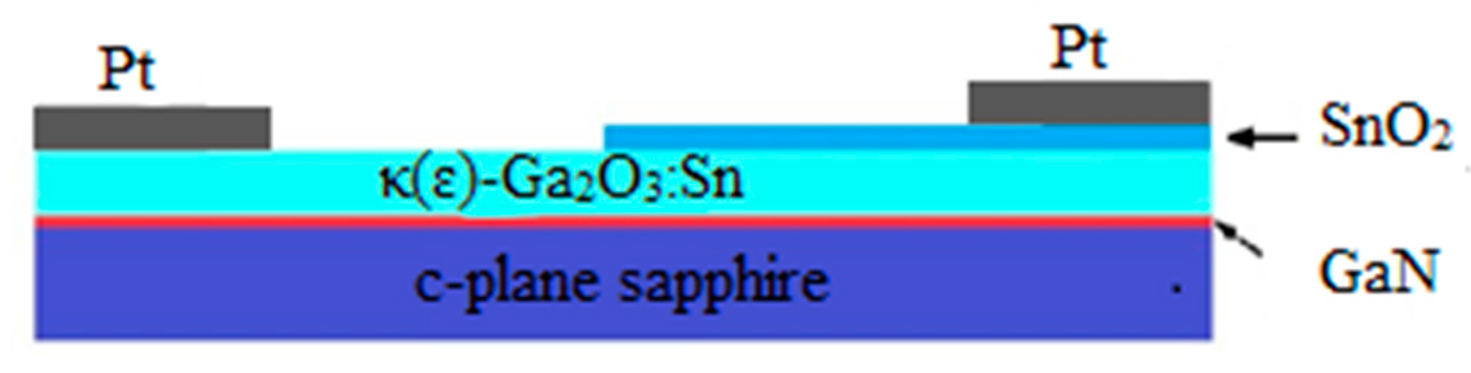
2. Materials and Methods

The following films were deposited on (0001) single crystal Al2O3 substrates: κ(ε)-Ga2O3:Sn and SnO2 thin films as well as SnO2/κ(ε)-Ga2O3:Sn heterostructure. The process of the κ(ε)-Ga2O3:Sn films growth was multistage. In the first stage, a 3-µm-thick semi-insulating (SI) GaN layer was deposited on the Al2O3 substrate by gas phase deposition employing a homemade reactor. This layer served as a template for the κ(ε)-Ga2O3:Sn film growth. In the second stage, a 1-µm-thick κ(ε)-Ga2O3 layer in situ doped by Sn was deposited on the SI-GaN layer by HVPE using a hot-wall homemade reactor. Gaseous gallium chloride and oxygen were utilized as precursors. The doping of the κ(ε)-Ga2O3 films was carried out during the growth by adding tin. The HVPE growth temperature of the κ(ε)-Ga2O3:Sn film was 600 °C. The analysis of current–voltage (IV) and capacitance–voltage (CV) characteristics applied at this stage showed that the effective donor concentration Nd of the films was 5.13 × 1020 cm−3.
120-nm-thick pure SnO2 thin films were deposited by means of magnetron sputtering of an Sn (5N) target in an oxygen–argon plasma on Al2O3 and κ(ε)-Ga2O3:Sn. An Edwards A-500 (Edwards, USA) setup was employed. To prepare SnO2/κ(ε)-Ga2O3:Sn heterostructures, SnO2 thin films were deposited through a mask with square-shaped slots of 1 mm × 1 mm. The temperature of substrates during the deposition of the film was RT. The working pressure and power were kept at 7 × 10⁻³ mbar and 70 W, respectively. The oxygen concentration in the O2+Ar mixture was 56.1 ± 0.5 vol. %. The as-deposited SnO2 films were annealed ex situ at T = 600 °C; for 4 hours in air. The estimates showed that the Nd value of these films was 5.26 × 1017 cm−3.
Pt contacts were deposited on the κ(ε)-Ga2O3:Sn and SnO2 films (see Figure 1) by means of the magnetron sputtering. Pt contacts were chosen on the basis of their high stability at high temperatures and under exposure to various gases, which are of natural surroundings- and industrial relevance.
X-ray diffraction (XRD) analysis of the samples was performed at DRON-6 diffractometer (Bourevestnik, Petersburg, Russia) equipped with a copper anode (CuKα1, λ = 1.5406 Å). The XRD patterns were registered in θ-2θ scanning mode. The phase composition of the samples was identified by the position of the reflection peaks. XRD θ-2θ curves were processed using the Scherrer method [20] to determine the characteristic size of the block in the direction perpendicular to the plane of epitaxial growth.
The chemical composition of the samples was studied by X-ray photoelectron spectroscopy (XPS). The XPS measurements were carried out using a hemispherical analyzer included in the ESCALAB 250Xi (Thermo Fisher Scientific, Waltham, MA, USA) laboratory spectrometer. The measurements were carried out using a monochromatized AlKa radiation (hv = 1486.6 eV). Survey and core (O1s, Sn3d, Ga3d) photoemission (PE) spectra were recorded at the analyzer transmission energy of 100 and 50 eV, respectively. The film’s surface was irradiated with argon ions at an average energy of 3 eV for 60 s before XPS measurements to remove adsorbed atoms and molecules of contaminants. The analysis of the core spectra was processed employing the Avantage Data System software.
Measurement of transmission spectra was carried out using an Ocean Optics (Ocean Insight, Orlando, FL, USA) spectrometric system to determine the Eg of SnO2 in the wavelength range of λ = 300–600 nm. The transmission spectrum of κ(ε)-Ga2O3:Sn films was measured using a UV-VIS two-beam SPECORD (Analytik Jena, Jena, Germany) spectrophotometer in the range of λ = 230–360 nm.
A high-resolution field emission scanning electron microscope (FESEM) Apreo 2S (Thermo Fisher Scientific, USA) operating at an accelerating voltage of 5 kV was employed to study the microrelief of the film surfaces with a high resolution.
Gas sensing measurements of the samples were performed in a dedicated sealed chamber with a volume of 100 cm3, equipped with a micro-probe Nextron MPS-CHH station (Nextron, Busan, Republic of Korea). A ceramic-type heater, installed in the sealed chamber, was used to heat the samples. The accuracy of temperature T control was ±0.1 °C. The experiments were carried out under dark conditions. Streams of pure dry air or gas mixture of pure dry air + H2 were pumped through the chamber to measure the gas sensing characteristics of the samples. The H2 concentration in the mixture was controlled by a gas mixing and delivery system Microgas F-06 (Intera, Moscow, Russia). A special generator (Khimelektonika SPE, Moscow, Russia) was used to produce pure dry air. The total flow rate of the gas mixtures through the chamber was 1000 sccm. The relative error of the gas mixture flow rate did not exceed 1.5%. A Keithley 2636 A (Keithley, Solon, OH, USA) source meter was utilized to measure the time dependences of the current I and the IV characteristics of the samples. An E4980A RLC-meter (Agilent, Santa Clara, CA, USA) was applied to measure the CV dependences. Additionally, gas sensing measurements of the samples were carried out under exposure to NH3, CH4, CO, NO2, and O2. A mixture of N2 + O2 was used to study the sensitivity of samples to O2. To study the effect of relative humidity (RH) on the response of the samples to H2, the pure dry air in one of the channels was passed through a bubbler with distilled water. Then it entered the homogenizer, where it was mixed with the pure dry air and/or pure dry air + H2 mixture streams from the other channels. Varying the ratio of flows through the channels, we set the desired level of RH in the measuring chamber. An HIH 4000 Honeywell capacitive sensor with an absolute error of ±3.5% was used to measure the RH. Just prior to these measurements, all the samples were subjected to heat treatment at T = 500 °C for 90 s in pure dry air to stabilize the contact properties and regenerate the surface.

3. Results and Discussion

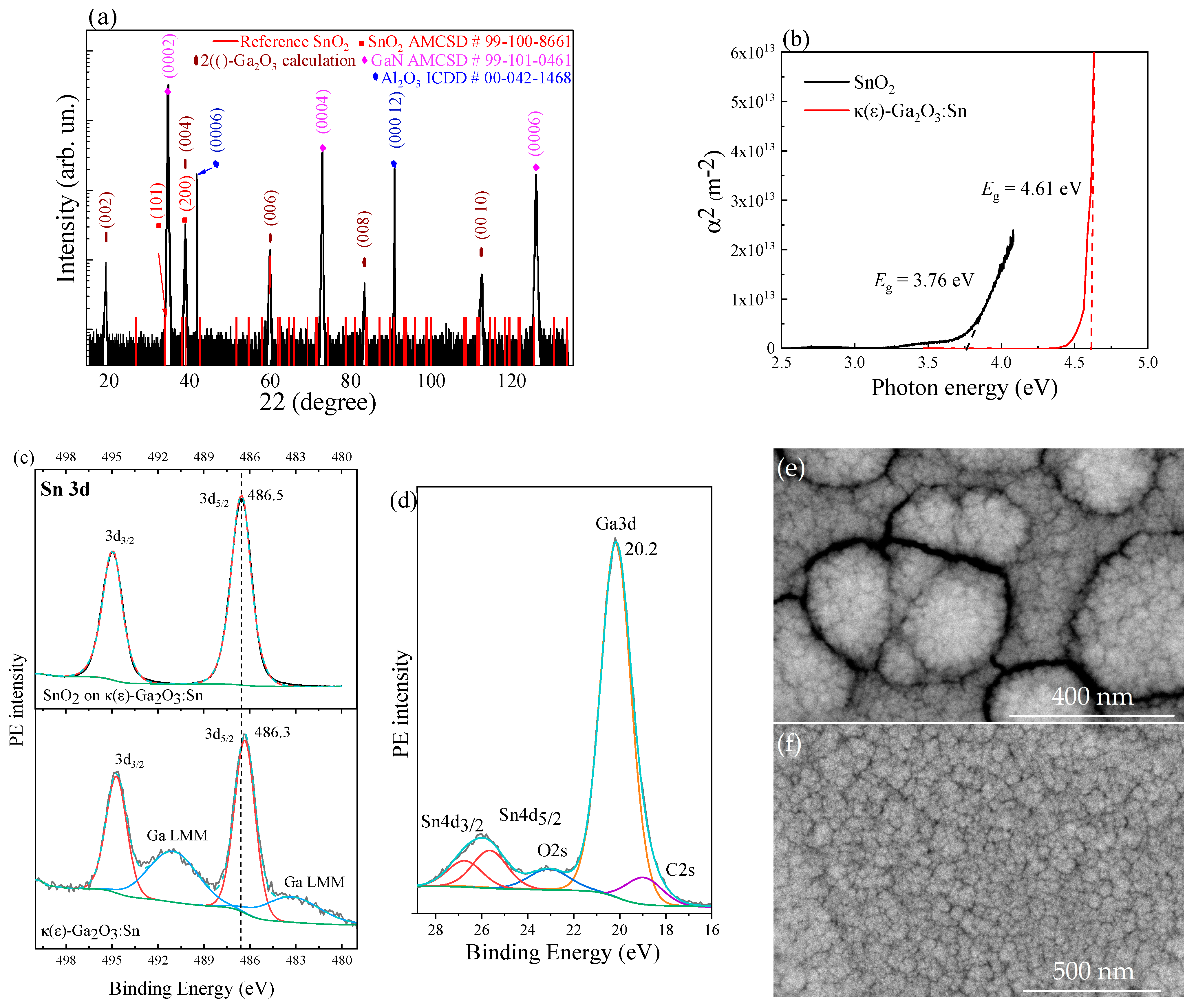
3.1. Structural Properties

Figure 2a illustrates the θ-2θ XRD pattern of the SnO2/Ga2O3 heterostructure deposited on an Al2O3 substrate via a GaN template. The peaks at 2θ = 41.8° and 90.9° are associated with the (0006) and (0 0 0 12) reflections of the Al2O3 substrate (ICDD # 00-042-1468). A series of peaks at 2θ = 19.2°, 39.0°, 60.0°, 83.6°, and 112.7° correspond to the 002, 004, 006, 008, and 0 0 10 planes of the κ(ε)-Ga2O3 phase. (The calculation was made on the basis of the Bragg equation for the case of CuKα1 anode (λ = 1.5406 Å). The peaks at 2θ = 34.7°, 73.0°, and 126.1° are due to the (0002), (0004), and (0006) reflections of the GaN template (AMCSD # 99-101-0461). Peaks corresponding to SnO2 could not be distinguished due to possible overlapping by neighboring reflections of other phases. Thus, the (101) reflection of SnO2 (AMCSD no. 99-100-8661) is close to the (0002) one of GaN, and the (111) reflection of SnO2 is close to the (004) one of κ(ε)-Ga2O3. The auxiliary vertical red lines of equal intensity depicted in Figure 2a are the tabular values of the SnO2 reflection positions. In addition, difficulties in SnO2 peaks identification may be caused by the low film thickness and the developed microrelief of the surface. Finally, the possible low crystallinity of the SnO2 phase may be the reason for the absence of sharp peaks on the XRD pattern. In this case, broad humps of a low intensity may be present.
κ(ε)-Ga2O3:Sn and SnO2 films are characterized by direct optical transitions according to the analysis of transmission spectra (see Figure 2b), where α is the absorption coefficient. Eg values were graphically calculated and proved to be equal to 4.61 ± 0.01 eV and 3.76 ± 0.01 eV for the κ(ε)-Ga2O3:Sn and SnO2 films, respectively.
According to XPS analysis, the composition of the SnO2 film includes Sn and O elements only. However, carbon (C) as a common contaminant was also observed in the subsurface layer a few nanometers thick. C atoms completely disappear after argon-etching for 60 s. Ga, Sn, O, and C lines were observed in the survey PE spectra of κ(ε)-Ga2O3:Sn film. The Sn concentration in this film appeared to be about 3 at. %, which indicates a high level of doping. Thus, the chemical analysis has shown that there are no third-party impurities in the composition of κ(ε)-Ga2O3:Sn and SnO2 films, which confirms the high purity of the deposited films.
The analysis of the chemical state of Sn based on the Sn3d5/2 PE line revealed the energy position of the main maximum of Sn at 486.5 and 486.3 eV (Figure 2c). The obtained values are in good agreement with the literature data [21,22] and correspond to the higher oxidation state of Sn–SnO2 oxide. A lower value of the SnO2 energy position for the κ(ε)-Ga2O3:Sn film indicates the effect of Ga2O3 on the charge state of SnO2. Previously, we have observed a similar effect of the Sn3d5/2 PE line shift to low binding energies of the SnO2 film doped with rare-earth elements and platinum group metals [21,22]. Analysis of the Ga chemical state in the κ(ε)-Ga2O3:Sn film based on the Ga3d PE line showed that Ga corresponds to the higher Ga2O3 oxide [23] (Figure 2d).
FESEM images of the SnO2 films surface deposited on Al2O3 substrates and κ(ε)-Ga2O3:Sn film are displayed in Figure 2e,f, respectively. The microrelief of the SnO2 film on Al2O3 (Figure 2e) contains small spherical grains with a diameter of ~35 nm and large agglomerates with a characteristic size of ~300 nm. Whereas the microrelief of the SnO2 film deposited on a κ(ε)-Ga2O3:Sn one (see Figure 2f) is represented by small grains with a diameter of ~35 nm only. The formation of large agglomerates for these structures was not observed.

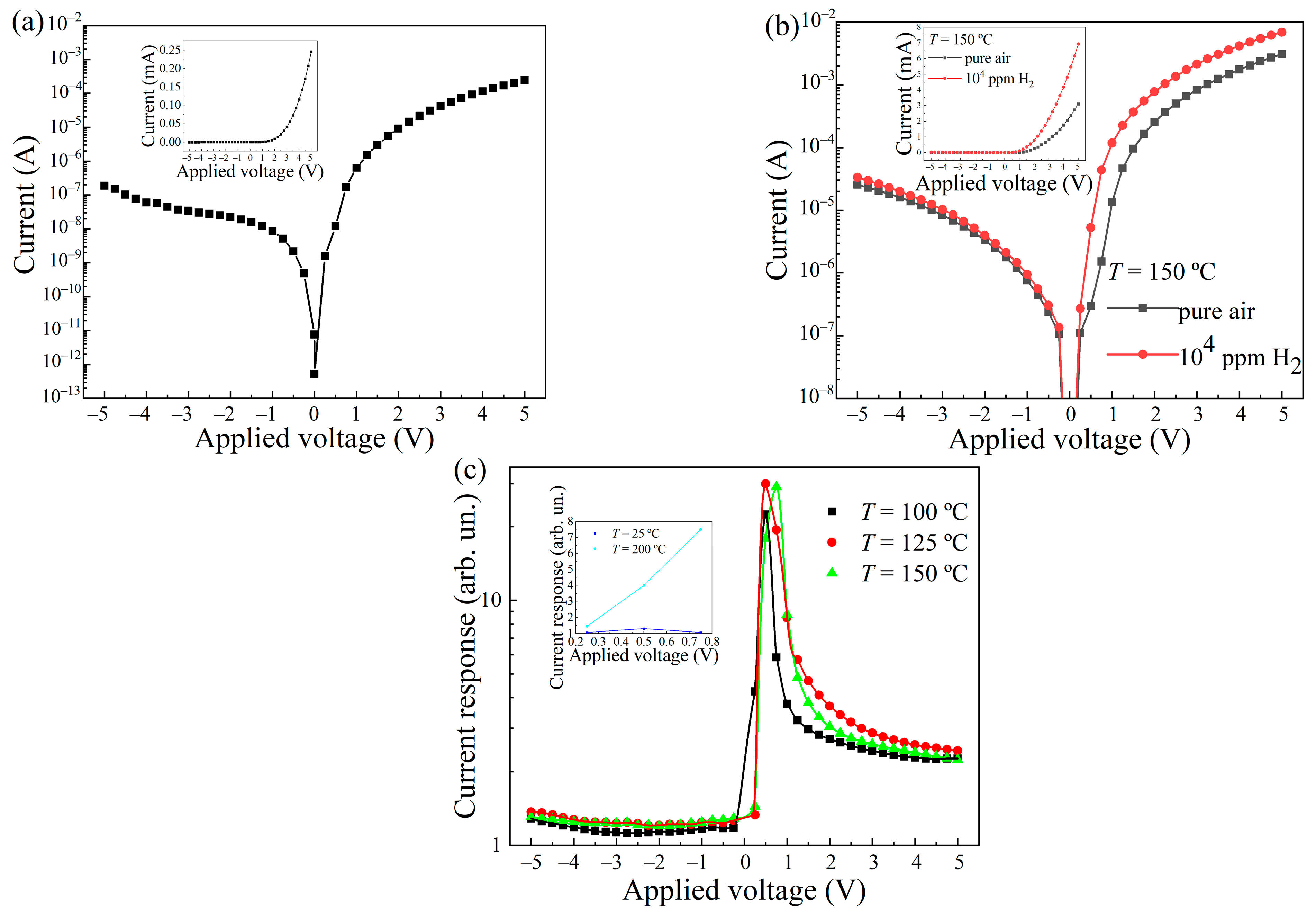
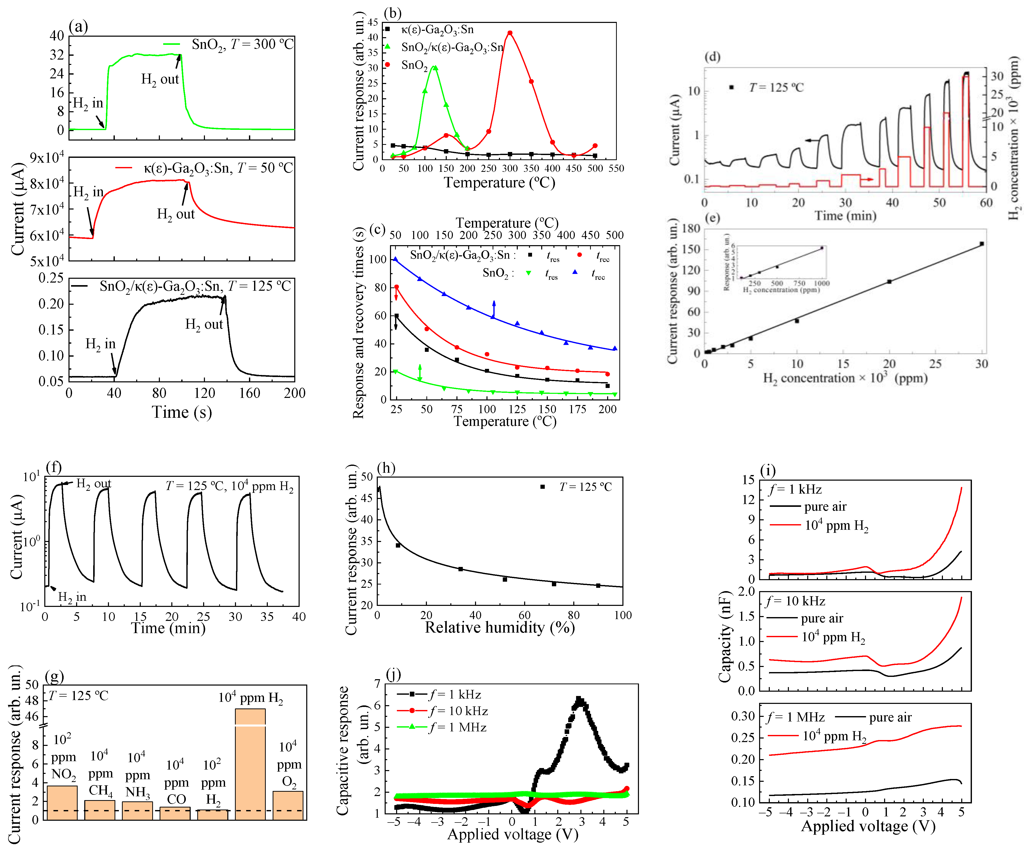
3.2. Gas-Sensitive Properties of the SnO2/κ(ε)-Ga2O3:Sn heterostructure

The IV characteristics of the SnO2 thin films equipped with Pt contacts are linear in the range of applied voltages U = −40–40 V at RT as well as at higher T. Contrary to this, the IV characteristics of the κ(ε)-Ga2O3:Sn films equipped with Pt contacts are nonlinear. The dependence of ln(I) on U1/4 is linear, indicating the presence of a Schottky barrier at the Pt/κ(ε)-Ga2O3:Sn interface [24]. The I value through the Pt/κ(ε)-Ga2O3:Sn/Pt structures exceeds 0.1 A at U > 12 V which leads to the samples self-heating.
The SnO2/κ(ε)-Ga2O3:Sn structure equipped with Pt contacts is a n-N isotype heterojunction and the Schottky barriers are connected in series. The IV characteristics of such heterostructures are nonlinear and asymmetric as can be seen in Figure 3a. The I(U = 4 V)/I(U = −4 V) ratio reaches the value of ~2 × 10³ at T = 25 °C, then drops by half as T increases to 150 °C. The increase in reverse current with T rising is significantly higher than the increase in forward current. The forward-bias region of the IV characteristics is approximated by the following function: If = A1 × exp(B1U), where If is a forward current; and A1 and B1 are the constants: A1 = (3.0 ± 0.4) × 10−6 A and B1 = 0.88 ± 0.02 V−1 at T = 25 °C. The reverse-bias region of the IV characteristics can be approximated by a similar function of Ir = A2 × exp(B2|U|), where Ir is a reverse current; A2 and B2 are the constants: A2 = (2.0 ± 0.4) × 10−9 A and B1 = 0.89 ± 0.04 V−1 at T = 25 °C. The forward-bias mode of the structure corresponds to the application of a positive potential to the SnO2/Pt interface.
Exposure to H2 leads to a reversible increase in the I through heterostructures at T = 25–200 °C. Figure 3b shows the change in the IV characteristics of the SnO2/κ(ε)-Ga2O3:Sn heterostructure when exposed to 104 ppm of H2 at T = 150 °C. The type of the functions, approximating the forward and reverse branches of the IV characteristics, does not change with increasing T to 200 °C and under exposure to 104 ppm of H2. The A1 and A2 increase, but B1 and B2 values decrease with T. The A1 and A2 values increase, whereas B1 and B2 practically do not change when exposed to H2. Table 1 shows the A1, A2, B1, and B2 values at T = 150 °C and under exposure to 104 ppm of H2.
To assess the effect of H2 on the I through the SnO2/κ(ε)-Ga2O3:Sn structures, the current response SI was calculated based on the experimental IV characteristics by the following ratio:
SI = IH/Iair,
where IH is the current of the charge carrier through the SnO2/κ(ε)-Ga2O3:Sn heterostructure in the gas mixture of pure dry air + H2; Iair is the current of the charge carrier through the SnO2/κ(ε)-Ga2O3:Sn heterostructure in pure dry air. The SI values calculated on the basis of the experimental IV characteristics and time dependences of currents at a fixed U (see Figure 4a) coincide. The SI value depends on the magnitude and direction of the applied voltage (see Figure 3c). The highest response in the range of T = 100–125 °C was observed at U = 0.5 V, whereas the highest SI was observed at U = 0.75 V at T = 150 °C. At room temperature, the maximum SI was also noticed at U = 0.5 V (see Figure 3c, insertion). The response decreases exponentially with the applied voltage in the range of U = 1–5 V. SI values are significantly lower at the reverse-bias mode and decrease slightly with an increase in the reverse voltage |Ur| from 0.25 V to 2.5 V. Moreover, the response increases slightly with a further increase in |Ur| to 5 V.
The temperature dependences of the sample’s response to 104 ppm of H2 are presented in Figure 4b. The κ(ε)-Ga2O3:Sn films show the highest response to H2 at T = 25 °C. The SI of κ(ε)-Ga2O3:Sn films exceeds those of SnO2 films in the temperature range of T = 25–50 °C; meanwhile, the SI of κ(ε)-Ga2O3:Sn films decreases and SI of SnO2 films increases drastically with further increase in T. Sensitivity of SnO2 and κ(ε)-Ga2O3:Sn films is based on reversible chemisorption of H2 molecules on the semiconductor’s surface according to the mechanisms described in refs. [14,25]. High sensitivity to H2 at moderate temperatures (T = 300 °C) is characteristic of the SnO2 thin films. Low SI for the κ(ε)-Ga2O3:Sn films are caused by a significant influence of the bulk conductivity Gb, which does not depend on the charge state of the surface. The dependence of the SnO2/κ(ε)-Ga2O3:Sn heterostructures response to H2 on temperature is characterized by a maximum at T = 125 °C. These samples demonstrate the highest SI in the range of T = 75–125 °C.
The experimental results displayed in Figure 4c prove that the SnO2/κ(ε)-Ga2O3:Sn heterostructures are characterized by the high speed of operation compared to the SnO2 thin films when exposed to H2. The response tres and recovery trec times were calculated to assess the speed of operation by the method described in ref. [9]. The calculated tres and trec values can only be used to compare the speed of sensors operation at similar experimental conditions. tres and trec decrease exponentially with T. trec and tres + trec of the SnO2/κ(ε)-Ga2O3:Sn structures are significantly lower than those of SnO2 thin films at T = 25–200 °C. SnO2 films are characterized by low tres. The speed of operation for the κ(ε)-Ga2O3:Sn films was not evaluated due to their low responses at T > 50 °C. These samples are of interest for developing room temperature H2 sensors. The tres and trec of these films under exposure to 104 ppm of H2 at T = 25 °C are 349.2 s and 379.6 s, respectively. Obviously, SnO2/κ(ε)-Ga2O3:Sn heterostructures are the most interesting for highly sensitive H2 sensors with high speed of operation and low operating temperatures. Therefore, our further attention will be focused on these structures.
The dependence of the SnO2/κ(ε)-Ga2O3:Sn structure response on the H2 concentration nH2 is linear (Figure 4d,e) in the nH2 range of 100–30000 ppm. The Iair and IH of the SnO2/κ(ε)-Ga2O3:Sn heterostructure decrease by 30% and 28%, respectively (see Figure 4f), during a cyclic exposure to H2 (five cycles). At the same time, the current response decreased by only 17%. The observed decrease in response during cyclic exposure to H2 is caused by the manifestation of chemisorbed hydrogen atoms with high binding energy. The temperature of 125 °C is not sufficient for the complete desorption of these hydrogen atoms from the semiconductor surface. Short-term heating of the structure at high temperatures can be used to regenerate the surface of semiconductors and for full desorption of H atoms [26]. The results of the long-term tests of the SnO2/κ(ε)-Ga2O3:Sn heterostructures at T = 125 °C and when exposed to 104 ppm of H2 demonstrated opposite changes of SI. The samples after the experiments were stored in sealed packages. The long-term tests lasted 8 weeks with an interval between the experiments of 7–8 days. Just prior to each measurement the SnO2/κ(ε)-Ga2O3:Sn heterostructures were subjected to heat at T = 500 °C for 90 s. There were increases in response from ~30 arb. un. to 47 arb. un. during the long-term tests. Response increases mostly due to a decrease in Iair. The most significant changes in response were in the first 4 weeks of testing.
The responses of the SnO2/κ(ε)-Ga2O3:Sn heterostructure to NO2, CH4, NH3, CO, and O2 gases at T = 125 °C was measured to evaluate its selectivity (Figure 4g). Noteworthy, is that I through heterostructure increases reversibly when exposed to 104 ppm of CH4, NH3h and CO. The response to these gases has been calculated by equation (1). The IH was replaced by Ig, where Ig is the charge carrier current through the SnO2/κ(ε)-Ga2O3:Sn heterostructure in the gas mixture of pure dry air + reducing gas (CH4, NH3, or CO). The responses to CH4, NH3, and CO are insignificant compared to the SI to H2, which equates to 29.92–46.98 arb. un. at T = 125 °C and nH2 = 104 ppm.
It was found, that the I value of the SnO2/κ(ε)-Ga2O3:Sn reversibly decreases when exposed to NO2 and O2. The responses to NO2 (SNO2) and O2 (SO2) have been calculated by the following equations, correspondently:
SNO2 = Iair/INO2,
SO2 = IN/IO2,
where INO2 is the charge carrier current through the SnO2/κ(ε)-Ga2O3:Sn heterostructure in the gas mixture of pure dry air + NO2; IN is the charge carrier current through the SnO2/κ(ε)-Ga2O3:Sn heterostructure in the nitrogen atmosphere; IO2 is the charge carrier current through the SnO2/κ(ε)-Ga2O3:Sn heterostructure in the gas mixture of N2 + O2. SI ratio when exposed to 100 ppm of H2 at T = 125 °C happened to be 26.7 times lower than those for 100 ppm of NO2 (Figure 4g). The SnO2/κ(ε)-Ga2O3:Sn heterostructure also demonstrated relatively high response to O2. The response to O2 appears to be higher than to CH4, NH3, or CO at same concentration values. Hence, we have shown that SnO2/κ(ε)-Ga2O3:Sn heterostructure is also attractive for developing highly sensitive NO2 and O2 sensors operating at low temperatures.
An increase in RH leads to a drop in the response of the SnO2/κ(ε)-Ga2O3:Sn heterostructure to H2 (Figure 4h). The most significant decrease in SI occurs when RH increases from 0 to 34 %. In the range of RH = 34–90.0%, the response varies slightly.
Furthermore, the effect of 104 ppm of H2 on the C-V characteristics of the SnO2/κ(ε)-Ga2O3:Sn heterostructures at T = 125 °C and signal frequencies f = 1 kHz, 10 kHz, and 1 MHz have been studied. The results are illustrated in Figure 4i,j. Evidently, exposure to H2 leads to a reversible increase in the electrical capacity of the structures. The capacitive response SC has been calculated by the following equation:
SC = CH/Cair,
where CH is the electrical capacitance of SnO2/κ(ε)-Ga2O3:Sn heterostructure in the gas mixture of pure dry air + H2; and Cair is the electrical capacitance of structures in pure dry air. Visibly, the SC (see Figure 4i) is significantly lower than the SI (Figure 3c). At f = 10 kHz and 1 MHz the capacitive response varies weakly. The highest SC value is observed in the range of U = 0.95–5.00 V at f = 1 kHz and has a maximum at U = 2.9 V.

3.3. The Mechanism of the Sensory Effect

Initially, the resistance of the Pt/κ(ε)-Ga2O3:Sn interface is low and the Pt/SnO2 contact is ohmic. The change in the potential barrier at Pt/κ(ε)-Ga2O3:Sn and Pt/SnO2 interfaces upon exposure to gases can be neglected. The observed high responses of the SnO2/κ(ε)-Ga2O3:Sn heterostructure at T = 25–175 °C; are due to the formation of the n-N isotypic heterojunction, where SnO2 is the base.
Diffusion of H atoms up to the SnO2/κ(ε)-Ga2O3:Sn interface at T = 25–175 °C; is unlikely. Changes of I and C upon exposure to H2 occur mainly due to the chemisorption of gas molecules on semiconductor’s surface. In the air atmosphere within a temperature range of T = 25–175 °C, the oxygen chemisorbs mainly in a molecular form on metal oxide semiconductors surface and captures electrons from their conduction band [25,27]. The reaction of reversible chemisorption of oxygen molecules can be represented as follows:
O2 + Sa + e ↔ O2(c),
where Sa is a free adsorption center; e is the electron charge; O2(c) is the chemisorbed oxygen ion. As a result of reaction (4), an electron-depleted region is formed in the near-surface part of the semiconductor. A negative charge on the surface causes the upward of energy bands bending at eVs, where Vs is the surface potential and eVs~Ni2, where Ni is the surface density of chemisorbed oxygen ions. In our case, the Debye length LD for SnO2 exceeds the grain size and the effect of grain boundaries on the transport of charge carriers in a semiconductor can be ignored. Oxygen chemisorption weakly changes the electrical conductivity of the κ(ε)-Ga2O3:Sn films due to the low contribution of the surface conductivity Gs to the total conductivity of Gt. Thus, changes in the current during the chemisorption of gases are mainly due to changes in the concentration of charge carriers in the SnO2.
Gt = Gb + Gs and the relationship between Gt and eVs in our case is described by the following equation [28]:
Gt = Gb × [1 − (LD/D) × [eVs/(kT)]],
where D is the SnO2 film thickness; k is the Boltzmann constant. An increase in the eVs due to the oxygen molecule’s chemisorption on the SnO2 surface leads to a drop of Gt. The increase in Gt when exposed to H2 is caused by the interaction of H2 molecules with previously chemisorbed O2(c) on the SnO2 surface. This interaction can be represented as follows:
2H2 + O2(c) → 2H2O + e.
As a result of reaction (7), a neutral H2O molecule is formed and desorbed, an electron returns to the conduction band of SnO2, the eVs decreases and the finally Gt increases. When exposed to NO2 the following reactions take place [29]:
NO2 + Sa + e → NO2,
NO2 → O(c) + NO,
O(c) + O(c) → O2(c) + e + Sa.
NO2 molecules chemisorb onto free adsorption centers and capture electrons from the SnO2 conduction band. Meanwhile, eVs is proportional to (Ni + NNO2)2 in the mixtures of air + NO2, where NNO2 is the surface density of chemisorbed NO2 ions [25,27]. An additional negative charge on the surface of the SnO2 film leads to a greater decrease in Gt. Further, NO2 ions are dissociated to form chemisorbed O(c) ions and gaseous NO molecules. In the low temperature region, atomic O(c) ions associated to O2(c) form and a free electron e, which returns to the conduction band of the semiconductor.
The κ(ε)-Ga2O3:Sn film is a source of electrons that are involved in reactions (5) and (8) with the gas molecules on the SnO2 surface. This causes a high response of heterostructure at T = 75–175 °C. The base region (SnO2) is filled with electrons from the κ(ε)-Ga2O3:Sn film with T rising, Gb of SnO2 increases and the response decreases. SnO2 films deposited on κ(ε)-Ga2O3:Sn are characterized by the absence of large agglomerates (see Figure 2e,f). This leads to an increase in the specific surface area of SnO2 and the surface density of adsorption centers for gas molecules.
Table 2 shows a comparison of the responses and optimal operating temperatures of structures based on the Ga2O3 polymorphs when exposed to H2 and NO2 [9,14,18,19,30,31,32,33,34,35,36,37,38,39,40,41,42]. ng is a gas concentration. SnO2/κ(ε)-Ga2O3:Sn heterostructure in comparison with other items listed in this table is characterized by relatively high sensitivity to H2 and NO2 at a relatively low operating temperature. Ga2O3-based structures with higher responses to gases are characterized by high operating temperatures [9,30,34,35,36,37,41,42], low speed of operation [18,19], or are diode-type sensors based on high-cost materials [31,32,39]. SnO2/κ(ε)-Ga2O3:Sn heterostructures demonstrate relatively high responses to H2 and NO2 at lower temperatures in comparison with the heterostructures based on other metal oxides (see Table 3). Nano-structured heterostructures are characterized by higher responses to NO2 but generally do not differ in high speed of operation.

4. Conclusions

The structural and gas-sensitive properties of the n-N SnO2/κ(ε)-Ga2O3:Sn heterostructures were investigated for the first time. The κ(ε)-Ga2O3:Sn and SnO2 films were obtained by the halide vapor phase epitaxy and the high-frequency magnetron sputtering, respectively. The κ(ε)-Ga2O3:Sn crystalline film has a bandgap of 4.61 ± 0.01 eV. The SnO2 nanocrystalline film has a bandgap of 3.76 ± 0.01 eV and is characterized by a developed microrelief of the surface, represented by grains with a size of ~35 nm. Exposure to H2 leads to an increase in electrical current and capacitance of SnO2/κ(ε)-Ga2O3:Sn structures. The current response of heterostructures to H2 significantly exceeds the capacitive one. Gas sensor response and speed of operation of the SnO2/κ(ε)-Ga2O3:Sn heterostructure under H2 exposure overperform those of the single κ(ε)-Ga2O3:Sn and SnO2 films in the temperature range of 25–175°C. This heterostructure demonstrates a low response to CO, NH3, and CH4 and a high response to NO2 even at low concentrations. The current responses of SnO2/κ(ε)-Ga2O3:Sn heterostructure to 104 ppm of H2 and 100 ppm of NO2 at 125 °C were 30–47 A.U. and 3.7 A.U., correspondingly. The sensory effect is realized mainly due to the chemisorption of gas molecules on the SnO2 surface, which is the base region of the heterostructure. The κ(ε)-Ga2O3:Sn film is a source of electrons that are involved in reactions with gas molecules on the SnO2 film surface. The SnO2 film deposited on the κ(ε)-Ga2O3:Sn film is characterized by a more developed surface microstructure. This leads to an increase in the surface density of adsorption centers for gas molecules. The advantages of the SnO2/κ(ε)-Ga2O3:Sn heterostructure for gas sensors are shown, the main one being high sensitivity at relatively low operating temperatures. Doubtfully, this structure has every chance of being the base of the sensor.

Author Contributions

Conceptualization, A.A. and V.N.; methodology, V.K., P.B., P.K., J.D., A.P., A.K. and E.Z.; software, V.K., P.B., P.K., J.D., A.P., A.K. and E.Z.; validation, A.A. and V.N.; formal analysis, A.A., N.Y., V.K., P.B., P.K., J.D., A.P., A.K. and E.Z.; investigation, N.Y., V.K., J.D., A.P., A.K. and E.Z.; resources, A.A., V.N., J.D., A.P., A.K. and E.Z.; data curation, A.A., N.Y., P.B., A.P., A.K. and E.Z.; writing—original draft preparation, A.A., V.N., P.B. and P.K.; writing—review and editing, A.A., N.Y., V.N., P.B., P.K. and J.D.; visualization, A.A., N.Y., P.B., P.K., A.P., A.K. and E.Z.; supervision, A.A. and V.N.; project administration, A.A.; funding acquisition, A.A. All authors have read and agreed to the published version of the manuscript.

Funding

This research was funded by the Russian Science Foundation, grant number 20-79-10043. Viktor Kopyev acknowledges the support of the grant under the Decree of the Government of the Russian Federation No. 220 of 9 April 2010 (Agreement No. 075-15-2022-1132 of 1 July 2022).

Institutional Review Board Statement

Not applicable.

Informed Consent Statement

Not applicable.

Data Availability Statement

All data that support the findings of this study are included within the article.

Acknowledgments

The FESEM investigations have been carried out using the equipment of Share Use Centre “Nanotech” of the ISPMS SB RAS. XPS studies were carried out using the equipment of the resource center “Physical Methods of Surface Investigation” (Saint Petersburg University Research Park). We are grateful to Bogdan Kushnarev from Research and Development Centre for Advanced Technologies in Microelectronics at National Research Tomsk State University for the deposition of tin oxide and platinum films.

Conflicts of Interest

The authors declare no conflict of interest.

References

  1. Das, S.; Jayaraman, V. SnO2: A comprehensive review on structures and gas sensors. Prog. Mater. Sci. 2014, 66, 112–255. [Google Scholar] [CrossRef]
  2. Zhu, J.; Xu, Z.; Ha, S.; Li, D.; Zhang, K.; Zhang, H.; Feng, J. Gallium Oxide for Gas Sensor Applications: A Comprehensive Review. Materials 2022, 15, 7339. [Google Scholar] [CrossRef] [PubMed]
  3. Zhai, H.; Wu, Z.; Fang, Z. Recent progress of Ga2O3-based gas sensors. Ceram. Int. 2022, 48, 24213–24233. [Google Scholar] [CrossRef]
  4. Gogova, D.; Suwardi, A.; Kuznetsova, Y.; Zatsepin, A.; Mochalov, L.; Nezhdanov, A.; Szyszka, B. Lanthanum-doped barium stannate-a new type of critical raw materials-free transparent conducting oxide. J. Adv. Appl. Phys. Res. 2017, 4, 1–8. [Google Scholar] [CrossRef]
  5. Jeon, H.M.; Leedy, K.D.; Look, D.C.; Chang, C.S.; Muller, D.A.; Badescu, S.C.; Vasilyev, V.; Brown, J.L.; Green, A.J.; Chabak, K.D. Homoepitaxial β-Ga2O3 transparent conducting oxide with conductivity σ = 2323 S cm−1. Appl. Mater. 2021, 9, 101105. [Google Scholar] [CrossRef]
  6. Dalapati, G.; Sharma, H.; Guchhait, A.; Chakrabarty, N.; Bamola, P.; Liu, Q.; Saianand, G.; Ambati, M.; Mukhopadhyay, S.; Dey, A.; et al. Tin oxide for optoelectronic, photovoltaic and energy storage devices: A review. J. Mater. Chem. A 2021, 9, 16621–16684. [Google Scholar] [CrossRef]
  7. Yang, S.; Lei, G.; Xu, H.; Lan, Z.; Wang, Z.; Gu, H. Metal Oxide Based Heterojunctions for Gas Sensors: A Review. Nanomaterials 2021, 11, 1026. [Google Scholar] [CrossRef]
  8. Mahmoud, W.E. Solar blind avalanche photodetector based on the cation exchange growth of β-Ga2O3/SnO2 bilayer heterostructure thin film. Sol. Energy Mater. Sol. Cells 2016, 152, 65–72. [Google Scholar] [CrossRef]
  9. Almaev, A.; Nikolaev, V.; Yakovlev, N.; Butenko, P.; Stepanov, S.; Pechnikov, A.; Scheglov, M.; Chernikov, E. Hydrogen sensors based on Pt/α-Ga2O3:Sn/Pt structures. Sens. Actuators B Chem. 2022, 364, 131904. [Google Scholar] [CrossRef]
  10. Polyakov, A.; Smirnov, N.; Shchemerov, I.; Yakimov, E.; Pearton, S.; Ren, F.; Chernykh, A.; Gogova, D.; Kochkova, A. Electrical Properties, Deep Trap and Luminescence Spectra in Semi-Insulating, Czochralski β-Ga2O3 (Mg). ECS J. Solid State Sci. Technol. 2019, 8, Q3019. [Google Scholar] [CrossRef]
  11. Gogova, D.; Ghezellou, M.; Tran, D.; Richter, S.; Papamichail, A.; Hassan, J.; Persson, A.; Persson, P.; Kordina, O.; Monemar, B.; et al. Epitaxial growth of β-Ga2O3 by hot-wall MOCVD. AIP Adv. 2022, 12, 055022. [Google Scholar] [CrossRef]
  12. Yakimov, E.; Polyakov, A.; Nikolaev, V.; Pechnikov, A.; Scheglov, M.; Yakimov, E.; Pearton, S. Electrical and Recombination Properties of Polar Orthorhombic κ-Ga2O3 Films Prepared by Halide Vapor Phase Epitaxy. Nanomaterials 2023, 13, 1214. [Google Scholar] [CrossRef] [PubMed]
  13. Biswas, M.; Nishinaka, H. Thermodynamically metastable α-, ε- (or κ-), and γ-Ga2O3: From material growth to device applications. APL Mater. 2022, 10, 060701. [Google Scholar] [CrossRef]
  14. Almaev, A.; Nikolaev, V.; Butenko, P.; Stepanov, S.; Pechnikov, A.; Yakovlev, N.; Sinyugin, I.; Shapenkov, S.; Scheglov, M. Gas sensors based on pseudohexagonal phase of gallium oxide. Phys. Status Solidi B 2021, 259, 2100306. [Google Scholar] [CrossRef]
  15. Nikolaev, V.; Stepanov, S.; Pechnikov, A.; Shapenkov, S.; Scheglov, M.; Chikiryaka, A.; Vyvenko, O. HVPE Growth and Characterization of ε-Ga2O3 Films on Various Substrates. ECS J. Solid State Sci. Technol. 2020, 9, 45014. [Google Scholar] [CrossRef]
  16. Parisini, A.; Mazzolini, P.; Bierwagen, O.; Borelli, C.; Egbo, K.; Sacchi, A.; Bosi, M.; Seravalli, L.; Tahraoui, A.; Fornari, R. Study of SnO/ɛ-Ga2O3 p–n diodes in planar geometry. J. Vac. Sci. 2022, 40, 42701. [Google Scholar] [CrossRef]
  17. Budde, M.; Splith, D.; Mazzolini, P.; Tahraoui, A.; Feldl, J.; Ramsteiner, M.; Wenckstern, H.; Grundmann, M.; Bierwagen, O. SnO/β-Ga2O3 vertical pn heterojunction diodes. Appl. Phys. Lett. 2020, 117, 252106. [Google Scholar] [CrossRef]
  18. Jang, Y.; Kim, W.; Kim, D.; Hong, S. Fabrication of Ga2O3/SnO2 core–shell nanowires and their ethanol gas sensing properties. J. Mater. Res. 2011, 26, 2322–2327. [Google Scholar] [CrossRef]
  19. Abdullah, Q.; Ahmed, A.; Ali, A.; Yam, F.; Hassan, Z.; Bououdina, M. Novel SnO2-coated β-Ga2O3 nanostructures for room temperature hydrogen gas sensor. Int. J. Hydrogen Energy 2021, 46, 7000–7010. [Google Scholar] [CrossRef]
  20. Boiko, M.; Sharkov, M.; Boiko, A.; Konnikov, S.; Bobyl, A.; Budkina, N. Investigation of the Atomic, Crystal, and Domain Structures of Materials Based on X-Ray Diffraction and Absorption Data: A Review. Technic. Phys. 2015, 60, 1575–1600. [Google Scholar] [CrossRef]
  21. Maksimova, N.; Sevastyanov, E.; Chernikov, E.; Korusenko, P.; Nesov, S.; Kim, S.; Biryukov, A.; Sergeychenko, N.; Davletkildeev, N.; Sokolov, D. Sensors based on tin dioxide thin films for the detection of pre-explosive hydrogen concentrations. Sens. Actuators B Chem. 2021, 341, 130020. [Google Scholar] [CrossRef]
  22. Maksimova, N.; Almaev, A.; Sevastyanov, E.; Potekaev, A.; Chernikov, E.; Sergeychenko, N.; Korusenko, P.; Nesov, S. Effect of Additives Ag and Rare-Earth Elements Y and Sc on the Properties of Hydrogen Sensors Based on Thin SnO2 Films during Long-Term Testing. Coatings 2019, 9, 423. [Google Scholar] [CrossRef]
  23. Mahmoodinezhad, A.; Janowitz, C.; Naumann, F.; Plate, P.; Gargouri, H.; Henkel, K.; Schmeißer, D.; Flege, J. Low-temperature growth of gallium oxide thin films by plasma-enhanced atomic layer deposition. J. Vac. Sci. Technol. A 2020, 38, 022404. [Google Scholar] [CrossRef]
  24. Elhadidy, H.; Sikula, J.; Franc, J. Symmetrical current–voltage characteristic of a metal–semiconductor–metal structure of Schottky contacts and parameter retrieval of a CdTe structure. Semicond. Sci. Technol. 2012, 27, 15006. [Google Scholar] [CrossRef]
  25. Gaman, V. Basic physics of semiconductor hydrogen sensors. Russ. Phys. J. 2008, 51, 425. [Google Scholar] [CrossRef]
  26. Korotcenkov, G.; Cho, B. Instability of metal oxide-based conductometric gas sensors and approaches to stability improvement (short survey). Sens. Actuators B 2011, 156, 527–538. [Google Scholar] [CrossRef]
  27. Afzal, A. β-Ga2O3 nanowires and thin films for metal oxide semiconductor gas sensors: Sensing mechanisms and performance enhancement strategies. J. Mater. 2019, 5, 542–557. [Google Scholar] [CrossRef]
  28. Simion, C.; Schipani, F.; Papadogianni, A.; Stanoiu, A.; Budde, M.; Oprea, A.; Weimar, U.; Bierwagen, O.; Barsan, N. Conductance Model for Single-Crystalline/Compact Metal Oxide Gas-Sensing Layers in the Nondegenerate Limit: Example of Epitaxial SnO2(101). ACS Sens. 2019, 4, 2420–2428. [Google Scholar] [CrossRef]
  29. Badalyan, S.; Rumyantseva, M.; Smirnov, V.; Alikhanyan, A.; Gaskov, A. Effect of Au and NiO catalysts on the NO2 sensing properties of nanocrystalline SnO2. Inorg. Mater. 2010, 46, 232–236. [Google Scholar] [CrossRef]
  30. Yakovlev, N.; Almaev, A.; Butenko, P.; Tetelbaum, D.; Mikhaylov, A.; Nikolskaya, A.; Pechnikov, A.; Stepanov, S.; Boiko, M.; Chikiryaka, À.; et al. Effect of Si+ Ion Implantation in α-Ga2O3 Films on Their Gas Sensitivity. IEEE Sens. J. 2022, 23, 1885–1895. [Google Scholar] [CrossRef]
  31. Jang, S.; Jung, S.; Kim, J.; Ren, F.; Pearton, S.J.; Baik, K.H. Hydrogen Sensing Characteristics of Pt Schottky Diodes on (−201) and (010) Ga2O3 Single Crystals. ECS J. Solid State Sci. Technol. 2018, 7, Q3180. [Google Scholar] [CrossRef]
  32. Nakagomi, S.; Yokoyama, K.; Kokubun, Y. Devices based on series-connected Schottky junctions and β-Ga2O3/SiC heterojunctions characterized as hydrogen sensors. J. Sens. Sens. Syst. 2014, 3, 231–239. [Google Scholar] [CrossRef]
  33. Fleischer, M.; Giber, J.; Meixner, H. H2-induced changes in electrical conductance of β-Ga2O3 thin-film systems. Appl. Phys. A. 1992, 54, 560–566. [Google Scholar] [CrossRef]
  34. Cuong, N.D.; Park, Y.W.; Yoon, S.G. Microstructural and electrical properties of Ga2O3 nanowires grown at various temperatures by vapor–liquid–solid technique. Sens. Actuators B. 2009, 140, 240–244. [Google Scholar] [CrossRef]
  35. Almaev, A.; Chernikov, E.; Novikov, V.; Kushnarev, B.; Yakovlev, N.; Chuprakova, E.; Oleinik, V.; Lozinskaya, A.; Gogova, D. Impact of Cr2O3 additives on the gas-sensitive properties of β-Ga2O3 thin films to oxygen, hydrogen, carbon monoxide, and toluene vapors. J. Vac. Sci. Technol. A 2021, 39, 23405. [Google Scholar] [CrossRef]
  36. Bausewein, A.; Hacker, B.; Fleischer, M.; Meixner, H. Effects of Palladium Dispersions on Gas-Sensitive Conductivity of Semiconducting Ga2O3 Thin-Film Ceramics. J. Am. Ceram. Soc. 1997, 80, 317–323. [Google Scholar] [CrossRef]
  37. Fleischer, M.; Kornely, S.; Weh, T.; Frank, J.; Meixner, H. Selective gas detection with high-temperature operated metal oxides using catalytic filters. Sens. Actuators B. 2000, 69, 205–210. [Google Scholar] [CrossRef]
  38. Almaev, A.; Nikolaev, V.; Stepanov, S.; Pechnikov, A.; Chikiryaka, A.; Yakovlev, N.; Kalygina, V.; Kopyev, V.; Chernikov, E. Hydrogen influence on electrical properties of Pt-contacted α-Ga2O3/ε-Ga2O3 structures grown on patterned sapphire substrates. J. Phys. D Appl. Phys. 2020, 53, 414004. [Google Scholar] [CrossRef]
  39. Yan, J.; Lee, C. Improved detection sensitivity of Pt/β-Ga2O3/GaN hydrogen sensor diode. Sens. Actuators B. 2009, 143, 192–197. [Google Scholar] [CrossRef]
  40. Park, S.; Kim, S.; Sun, G.-J.; Lee, C. Synthesis, structure and ethanol sensing properties of Ga2O3-core/WO3-shell nanostructures. Thin Solid Films. 2015, 591, 341–345. [Google Scholar] [CrossRef]
  41. Jin, C.; Park, S.; Kim, H.; Lee, C. Ultrasensitive multiple networked Ga2O3-core/ZnO-shell nanorod gas sensors. Sens. Actuators B 2012, 161, 223–228. [Google Scholar] [CrossRef]
  42. Zhang, B.; Lin, H.; Gao, H.; Lu, X.; Nam, C.; Gao, P. Perovskite-sensitized β-Ga2O3 nanorod arrays for highly selective and sensitive NO2 detection at high temperature. J. Mater. Chem. A 2020, 8, 10845–10854. [Google Scholar] [CrossRef]
  43. Hu, J.; Sun, Y.J.; Xue, Y.; Zhang, M.; Li, P.W.; Lian, K.; Zhuiykov, S.; Zhang, W.D.; Chen, Y. Highly sensitive and ultra-fast gas sensor based on CeO2-loaded In2O3 hollow spheres for ppb-level hydrogen detection. Sens. Actuators B 2018, 257, 124–135. [Google Scholar] [CrossRef]
  44. Park, S.; Ko, H.; Kim, S.; Lee, C. Role of the interfaces in multiple networked one-dimensional core-shell nanostructured gas sensors. ACS Appl. Mater. Interfaces 2014, 6, 9595–9600. [Google Scholar] [CrossRef] [PubMed]
  45. Weber, M.J.; Kim, Y.; Lee, J.; Kim, J.; Iatsunskyi, I.; Coy, E.; Miele, P.; Bechelany, M.; Kim, S. Highly efficient hydrogen sensors based on Pd nanoparticles supported on boron nitride coated ZnO nanowires. J. Mater. Chem. A 2019, 7, 8107–8116. [Google Scholar] [CrossRef]
  46. Raza, M.; Kaur, N.; Pinna, E.C.N. Toward optimized radial modulation of the space-charge region in one-dimensional SnO2–NiO core-shell nanowires for hydrogen sensing. ACS Appl. Mater. Interfaces 2020, 12, 4594–4606. [Google Scholar] [CrossRef]
  47. Zhang, X.; Sun, J.; Tang, K.; Wang, H.; Chen, T.; Jiang, K.; Zhou, T.; Quan, H.; Guo, R. Ultralow detection limit and ultrafast response/recovery of the H2 gas sensor based on Pd-doped rGO/ZnO-SnO2 from hydrothermal synthesis. Microsyst. Nanoeng. 2022, 8, 67. [Google Scholar] [CrossRef]
  48. Anand, K.; Singh, O.; Singh, M.; Kaur, J.; Singh, R. Hydrogen sensor based on graphene/ZnO nanocomposite. Sens. Actuators B 2014, 195, 409–415. [Google Scholar] [CrossRef]
  49. Lupan, O.; Ababii, N.; Mishra, A.K.; Bodduluri, M.T.; Magariu, N.; Vahl, A.; Krüger, H.; Wagner, B.; Faupel, F.; Adelung, R.; et al. Heterostructure-based devices with enhanced humidity stability for H2 gas sensing applications in breath tests and portable batteries. Sens. Actuators A 2021, 329, 112804. [Google Scholar] [CrossRef]
  50. Sun, J.; Sun, L.; Han, N.; Pan, J.; Liu, W.; Bai, S.; Feng, Y.; Luo, R.; Li, D.; Chen, A. Ordered mesoporous WO3/ZnO nanocomposites with isotype heterojunctions for sensitive detection of NO2. Sens. Actuators B 2019, 285, 68–75. [Google Scholar] [CrossRef]
  51. Bai, S.; Li, D.; Han, D.; Luo, R.; Chen, A.; Chung, C. Preparation, characterization of WO3–SnO2 nanocomposites and their sensing properties for NO2. Sens. Actuators B 2010, 150, 749–755. [Google Scholar] [CrossRef]
  52. Hung, N.; Chinh, N.; Nguyen, T.; Kim, E.; Choi, G.; Kim, C.; Kim, D. Carbon nanotube-metal oxide nanocomposite gas sensing mechanism assessed via NO2 adsorption on n-WO3/p-MWCNT nanocomposites. Ceram. Int. 2020, 46, 29233–29243. [Google Scholar] [CrossRef]
  53. Barthwal, S.; Singh, B.; Singh, N.B. ZnO-SWCNT nanocomposite as NO2 gas sensor. Mater. Today Proc. 2018, 5, 15439–15444. [Google Scholar] [CrossRef]
  54. Du, W.; Wu, L.; Zhao, J.; Si, W.; Wang, F.; Liu, J.; Liu, W. Engineering the surface structure of porous indium oxide hexagonal nanotubes with antimony trioxide for highly-efficient nitrogen dioxide detection at low temperature. Appl. Surf. Sci. 2019, 484, 853–863. [Google Scholar] [CrossRef]
  55. Yang, Z.; Zhang, D.; Chen, H. MOF-derived indium oxide hollow microtubes/MoS2 nanoparticles for NO2 gas sensing. Sens. Actuators B 2019, 300, 127037. [Google Scholar] [CrossRef]
  56. Teng, L.; Liu, Y.; Ikram, M.; Liu, Z.; Ullah, M.; Ma, L.; Zhang, X.; Wu, H.; Li, L.; Shi, K. One-step synthesis of palladium oxide-functionalized tin dioxide nanotubes: Characterization and high nitrogen dioxide gas sensing performance at room temperature. J. Colloid Interface Sci. 2019, 537, 79–90. [Google Scholar] [CrossRef] [PubMed]
  57. Choi, H.; Kwon, S.; Lee, W.; Im, K.; Kim, T.; Noh, B.; Park, S.; Oh, S.; Kim, K. Ultraviolet Photoactivated Room Temperature NO2 Gas Sensor of ZnO Hemitubes and Nanotubes Covered with TiO2 Nanoparticles. Nanomaterials 2020, 10, 462. [Google Scholar] [CrossRef]
  58. Zhao, C.; Bai, J.; Gong, H.; Liu, S.; Wang, F. Tailorable morphology of core-shell nanofibers with surface wrinkles for enhanced gas-sensing properties. ACS Appl. Nano Mater. 2018, 1, 6357–6367. [Google Scholar] [CrossRef]
  59. Xie, J.; Liu, X.; Jing, S.; Pang, C.; Liu, Q.; Zhang, J. Chemical and electronic modulation via atomic layer deposition of NiO on porous In2O3 films to boost NO2 detection. ACS Appl. Mater. Interfaces 2021, 13, 39621–39632. [Google Scholar] [CrossRef]
Figure 1. Schematic of the SnO2/κ(ε)-Ga2O3:Sn heterostructure.
Chemosensors 11 00325 g001
Figure 2. Structural characterization of the samples: (a) XRD pattern of the SnO2/Ga2O3 heterostructure grown on GaN/Al2O3; (b) α2 versus the photon energy for κ(ε)-Ga2O3:Sn and SnO2 films; (c) Sn3d PE spectra of κ(ε)-Ga2O3:Sn and SnO2 films; (d) Ga 3d, Sn 4d PE lines for κ(ε)-Ga2O3:Sn; FESEM images of the SnO2 film deposited on Al2O3 (e) and κ(ε)-Ga2O3:Sn (f).
Chemosensors 11 00325 g002
Figure 3. IV characteristics of the SnO2/κ(ε)-Ga2O3:Sn heterostructure at T = 25 °C in pure dry air in semi-logarithmic coordinates (a), at T = 150 °C under exposure to 104 ppm of H2 (b). The insertions show these IV characteristics in linear coordinates. Dependence of the response to 104 ppm H2 on the applied voltage at different temperatures (c), the insertion shows the response to 104 ppm H2 on the applied voltage at T = 25 °C and 200 °C.
Chemosensors 11 00325 g003
Figure 4. Gas-sensitive properties of n-N SnO2/κ(ε)-Ga2O3:Sn heterostructure and other samples: (a) time dependences of current upon exposure to 104 ppm of H2; (b) temperature dependences of responses to 104 ppm of H2; (c) temperature dependences of response and recovery times upon exposure to 104 ppm of H2 for different samples; (d) time dependence of current upon exposure to different H2 concentration; (e) dependence of response on H2 concentration; (f) time dependence of current upon cyclic exposure to 104 ppm of H2; (g) responses to fixed concentrations of NO2, CH4, NH3, CO, H2, and O2; (h) effect of the relative humidity on responses to 104 ppm of H2; (i) dependences of the capacitive response on applied voltage upon exposure to 104 ppm of H2 at T = 125 °C and different frequencies; (j) effect of 104 ppm of H2 on C-V characteristics at T = 125 °C and different frequencies; dependences in (dh) were measured at T = 125 °C and U = 0.5 V.
Chemosensors 11 00325 g004
Table 1. A1, A2, B1, and B2 at T = 150 °C and under exposure to 104 ppm H2.
ConditionsA1 (A)A2 (A)B1 (V−1)B2 (V−1)
Dry pure air(1.1 ± 0.1) × 10−4(1.1 ± 0.1) × 10−60.65 ± 0.030.65 ± 0.02
Dry pure air + 104 ppm H2(2.6 ± 0.3) × 10−4(1.3 ± 0.1) × 10−60.66 ± 0.030.63 ± 0.03
Table 2. Gas-sensitive characteristics of structures based on Ga2O3 polymorphs.
Structureng (ppm)T (℃)Response (arb. un.)Ref.
H2
α-Ga2O3:Sn10435080[9]
α-Ga2O3:Si3 × 10440069.3[30]
β-Ga2O3500RT7.9 × 105[31]
β-Ga2O32000500ΔI = 1.4 (mA)[32]
β-Ga2O33 × 1046004[33]
β-Ga2O32003006.3[34]
β-Ga2O3:Cr2O3250050060[35]
β-Ga2O3/Pd nanoclusters104625~103[36]
β-Ga2O3/SiO2 (filter)5000700~103[37]
α-Ga2O3/κ(ɛ)-Ga2O3:Sn25001251.25[38]
κ(ɛ)-Ga2O31045009.44[14]
κ(ɛ)-Ga2O3:Sn104RT1.2
Pt/β-Ga2O3/GaN1000RT229.8[39]
β-Ga2O3/SnO210004008[18]
β-Ga2O3/SnO210002007075.5[19]
β-Ga2O3/WO310002004.1[40]
SnO2/κ(ε)-Ga2O3:Sn10001255.7This work
10447
NO2
β-Ga2O3/ZnO1030073.5[41]
β-Ga2O32008005.1[42]
β-Ga2O3/La0.8Sr0.2CoO325.7
SnO2/κ(ε)-Ga2O3:Sn1001253.7This work
Table 3. Gas-sensitive characteristics of heterostructures based on different metal oxide semiconductors.
Structureng (ppm)T (℃)Response (arb. un.)Ref.
H2
CeO2/In2O35016020.7[43]
SnO2/ZnO10035018.4[44]
Pd/BN/ZnO5020013[45]
SnO2/NiO500500114[46]
rGO/ZnO-SnO21003809.4[47]
RGO/ZnO2001503.5[48]
Al2O3/CuO1003002.37[49]
SnO2/κ(ε)-Ga2O3:Sn10001255.7This work
10447
NO2
m-WO3/ZnO1150167.8[50]
WO3/SnO2200200186[51]
WO3/MWCNT composite515018[52]
ZnO/SWCNT composite501505[53]
Sb2O3/In2O3 nanotubes18047[54]
MoS2/In2O3 nanotubes50RT209[55]
PdO/SnO2 nanotubes100RT20.3[56]
TiO2/ZnO nanotubes5RT2.05[57]
In2O3/ZnO5020078[58]
NiO/In2O310145532[59]
SnO2/κ(ε)-Ga2O3:Sn1001253.7This work
Disclaimer/Publisher’s Note: The statements, opinions and data contained in all publications are solely those of the individual author(s) and contributor(s) and not of MDPI and/or the editor(s). MDPI and/or the editor(s) disclaim responsibility for any injury to people or property resulting from any ideas, methods, instructions or products referred to in the content.

