1. Introduction
Research related to the harvesting, conversion, transmission and storage of electricity from decentralized sources is becoming increasingly relevant in view of the growing standard of living and energy needs of people. At the same time, the development of industrial technologies and society as a whole leads to an increasing amount of electricity, which is not consumed directly but is converted with parameters other than those of the electricity grid. On the other hand, with the continuous growth of the population and the quality of life of the people, the issues and decisions related to the rational use of resources, the protection of the environment and the maintenance of the ecological balance in nature are becoming more important [
1,
2].
Therefore, the sustainable development of society largely depends on maintaining a balance between the trends associated with increasing electricity consumption and declining primary energy sources. Their combination is possible only with the creation of innovations and the implementation of scientific and applied research in the field of power electronic converters (PEC) [
3,
4,
5].
Research in the field of using modern methods for the design of PEC is a major factor in the implementation of environmental policies. Improving electricity conversion efficiency by just a few percent at current global consumption volumes will lead to savings significantly exceeding the total energy production of a number of small countries such as Bulgaria while reducing harmful emissions and resources used.
On the other hand, ensuring the output indicators of the PEC is important for achieving the desired quality of the energy conversion process. Modern methods for the design and prototyping of PEC with guaranteed indicators require the use of a systematic approach—from formulating the problems to obtaining the final product and are related to the use of information and communication technologies and especially techniques, based on artificial intelligence [
6,
7,
8,
9]. A very detailed classification of artificial intelligence techniques applied in power electronics is given in [
7]. The paper presents an overview of artificial intelligence (AI) applications for power electronic systems depending on the three distinct phases of the product life cycle: design, control and maintenance. These phases are related to one or more tasks to be solved by AI: optimization, classification, regression and data structure exploration. Specific applications of four categories of AI are discussed: expert systems, fuzzy logic, metaheuristics, and machine learning. The generalizations and conclusions are drawn from a survey of over 500 publications on the topic to identify common understandings, practical implementation challenges, and research opportunities in the application of AI to power electronics. In this sense, as a functional layer between AI and the specific applications of power electronic systems, optimization is described as a tool for finding an optimal solution that maximizes or minimizes objective functions from a set of available alternatives, given constraints conditions, equalities, or inequalities to which solutions must conform. For example, in the design task, optimization serves as a tool to explore the optimal set of parameters that maximize or minimize the goals and constraints set in the design.
In [
10], by using expert systems (ES), fuzzy logic (FL) and artificial neural networks (ANN or NNW), the automated design of a modern wind energy system and its health monitoring in operating conditions, identification of smart grid subsystem failure models and smart control based on a real-time simulator. In [
11], an optimal design of a Full-Bridge CLLC Converter is given, based on the use of a Particle Swarm Optimization (PSO) algorithm. The goal is to increase device efficiency by reducing switching losses [
12] presents a new approach to the design and optimization of power electronic devices, in which the optimal characteristics of the circuit elements of a DC-DC converter are selected considering a certain objective function and various design constraints. Extensive amounts of component data available on commercial distributor sites have been used to train supervised machine-learning regression models. Thus, the use of machine learning-based techniques allows the data-driven optimization task to become amenable to a large design space. The developed tool can be used to compare the performance of a choice of converter topologies or of the specific technologies by which the semiconductor switches are manufactured, and also to predict the performance contribution of individual components. As an example, optimized 48-to-12 V, 5 A DC/DC converter designs based on GaN and Si MOSFETs are compared in terms of loss, size, and cost. In [
13] demonstrates a data-driven approach to capture values and characteristics of semiconductor switches and passive components used in power electronic converters. Large volumes of data on electronic components available from commercial distributors’ sites have been collected and processed to determine relationships between component characteristics that extend the bases of the description of physical process models. The data are used to train supervised regression machine learning models that can be used to predict component parameters. One practical use of these machine learning-based models is in an optimization tool that advises power electronic device designers on component selection to achieve optimal design under a given objective function. In [
14], a new model is proposed that simulates a hybrid power conversion system using a unified evolutionary algorithm (EA). This unified evolutionary algorithm is developed to incorporate the properties of differential evolution (DE) and genetic algorithm (GA). This study describes a modified hybrid power converter that optimizes the zero ripple (DZ) duty cycle through the proposed input ripple minimization algorithm. In [
15] presents the implementation of a random forest algorithm applied to decision-making in the design of power electronic converters. The algorithm is used to help choose the topology of the power circuit. The presented algorithm can be applied to isolated and non-isolated. All steps of the algorithm are described in detail, including training and testing data for designing a specific power electronic device. In [
16], a specialized algorithm for an expert system for choosing a power electronic converter topology is presented. The algorithm is aimed at providing optimal topology suggestions for a single-phase power factor correction converter in terms of preferred levels of efficiency, cost, and dimensions. The algorithm was developed using neural networks and a procedurally generated decision training database built using datasets of existing semiconductor and magnetic devices. The results of the verification and evaluation of the accuracy of the algorithm are presented.
From the review and analysis of the existing methods and their implementing algorithms for the optimal design of power electronic devices and systems based on the application of artificial intelligence techniques, it follows that in the prevailing cases, they are based on the collection and processing of data related to with training and implementation of complex procedures. In this regard, due to the specificity of electromagnetic processes (switching of the structure of the power circuit during operation), the design of power electronic devices based on the application of artificial intelligence techniques and data-driven models is practically very difficult to implement. On the other hand, the application of specialized design methods, which are based on analysis in an established mode of operation, without taking into account the transient processes in the power circuits, leads to the realization of devices with poor dynamic indicators and operational characteristics.
The main idea that is being developed is the design methodology to realize the implementation of standard tools and application programs in mathematical software widely used by engineers, such as Matlab, thus, allowing specialists with not very deep knowledge of mathematics and programming to apply state-of-the-art tools for designing and prototyping power electronic devices and systems. On the other hand, the main idea of model-based optimization is to achieve the maximum possible power scheme during its design and to teach a device with the best possible and guaranteed indicators. Of course, this approach does not negate the advantages offered by the optimal control synthesis for the realization of power electronic devices with improved characteristics. A number of studies prove that the optimally designed power scheme supports both control synthesis and controller tuning, as well as the required hardware and software resources for its implementation [
6,
7,
8]. The motivation for the creation of this manuscript is related to the fact that, at this moment, there is a lack of up-to-date research devoted to the methodological aspect of the design of power electronic devices and systems, as well as to present rational methodologies for their design, giving a possibility to formalize and automate the design process.
In this aspect, the aim of the present work is to offer a rational procedure for the design of power electronic devices and systems, which combines classical methods with modern achievements of modeling, computational mathematics and information and communication technologies. At the heart of this approach is the combination of design methodologies, knowledge derived from the experience of the designer and optimization. In this approach, the description of the building elements, structures and schemes of PEC is conducted with mathematical and information models, and the guarantee of the output indicators is conducted already in the process of designing the devices. The manuscript is organized as follows: the first part describes the main challenges and problems in the design of power electronic devices and systems. Various examples of optimal design are considered; The second part is dedicated to the model-based approach to the design of power electronic devices and systems; In the third part, the principle of operation and the main ratios used to design a resonant DC-DC converter are discussed; In the fourth part, the first optimization problem used to determine the circuit elements of the power circuit is formulated. This task is solved using standard Matlab/Simulink built-in functions; In the fifth chapter, the optimization problem is developed by adding additional conditions regarding the state variables. An algorithm and an author’s program are proposed, which gives the optimal values in the preset working interval; in the sixth chapter and seventh parts, discussion, conclusion and directions for research development are given.
2. Model-Based Design of Power Electronic Converters
Trends in the design and development of PEC are mainly related to guaranteeing the output indicators; reducing their dimensions, mass, and price; increasing reliability and service life. All this makes the task of optimal design in power electronics very difficult. It is impossible to solve it successfully without using advanced methods in combination with classical approaches. On the other hand, the accelerated development of computational mathematics and the computing power of mass and accessible hardware systems favors the penetration of information and communication technologies in the research of power electronics.
Most of the methods used to design the PEC can be summarized as follows [
17,
18,
19,
20,
21,
22]:
Based on generally accepted average estimates of state space after reaching a quasi-static state, not always guaranteeing the validity of their values in different operating modes.
As a result of the design, values of the building elements are reached, which are physically unrealizable as a consequence, the prototypes are selected as close as possible to the values thus determined. This requires repeated repetition of the calculation procedure until the design assignment is met or until it changes in the direction of loosening the initial requirements.
It is practically impossible to account for the complex influence of nonlinearities, it is practically impossible to take into account the complex influence of the nonlinearities, the variations of the nominal values of the parameters and their change during operation as a function of external disturbances change of supply voltage, ambient temperature, load and aging of elements.
If we take into account the relationship between the choice of parameters and the dynamics of the PEC, the amplitude values of currents and voltages on the building elements, it prolongs the process of selecting elements and is not guaranteed to find a solution to the problem.
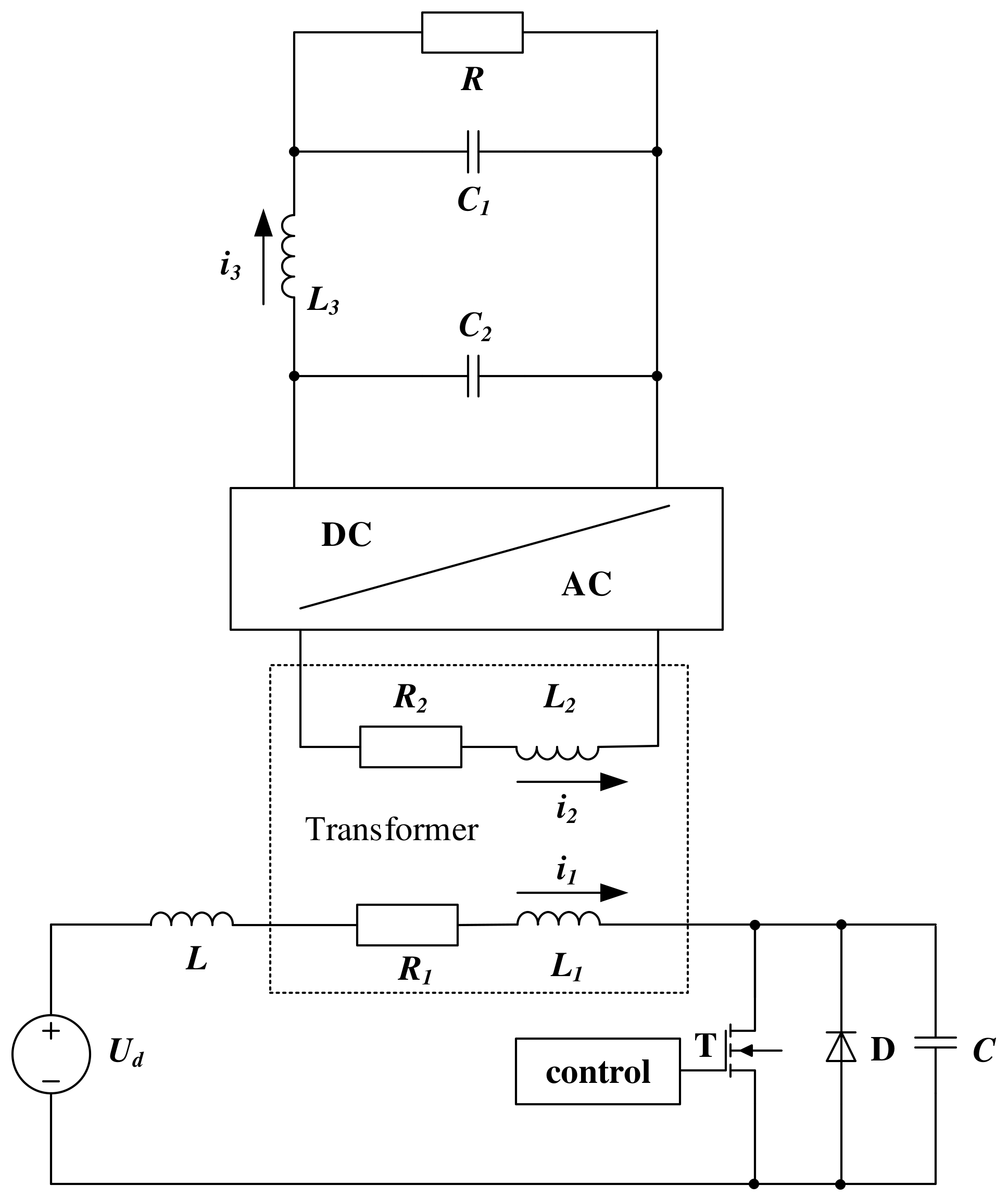
The manuscript proposes a design approach based on a combination of tools using basic relationships to obtain the initial values of the circuit elements obtained by analyzing the determined processes in the circuit and applying mathematical modeling and optimization to finally find the values of circuit elements. The basis of the second part of this method (finally finding) is the creation, verification and optimization of a model of the power scheme; therefore, it is called model-based design. The advantages of the method will be illustrated based on series single-ended transistor resonant DC-DC converters with soft switching (ZVS). The scheme of this device is shown in
Figure 1, being original and having a patent for invention [
23]. It is composed of an active-capacitive load (
C1 and
R), transistor T, resonant elements—capacitor
C and inductance
L, diode D, necessary in cases where the transistor does not have a built-in reverse diode, transformer, bridge rectifier, filter capacitance
C2 and inductance
L3. The analysis is carried out under the assumption of the ideality of all elements in the power circuit and also that the DC power source has zero internal resistance.
These schemes were chosen because no methodologies have been developed for their design due to the complexity of the power scheme, as well as the high order of differential equations that describe electromagnetic processes. In addition, the passage through the various stages of the operation of the power circuit is not determined only by externally controlled switching of the transistor, but directly depends on the operating mode and load parameters.
On the other hand, the creation of such a methodology requires efforts both for its development and for its adaptation for the purposes of power electronics. Thus, these circuits are a good example of illustrating the advantages of using model-based design in power electronics.
3. Description and Modeling of Power Circuit
The power circuits of
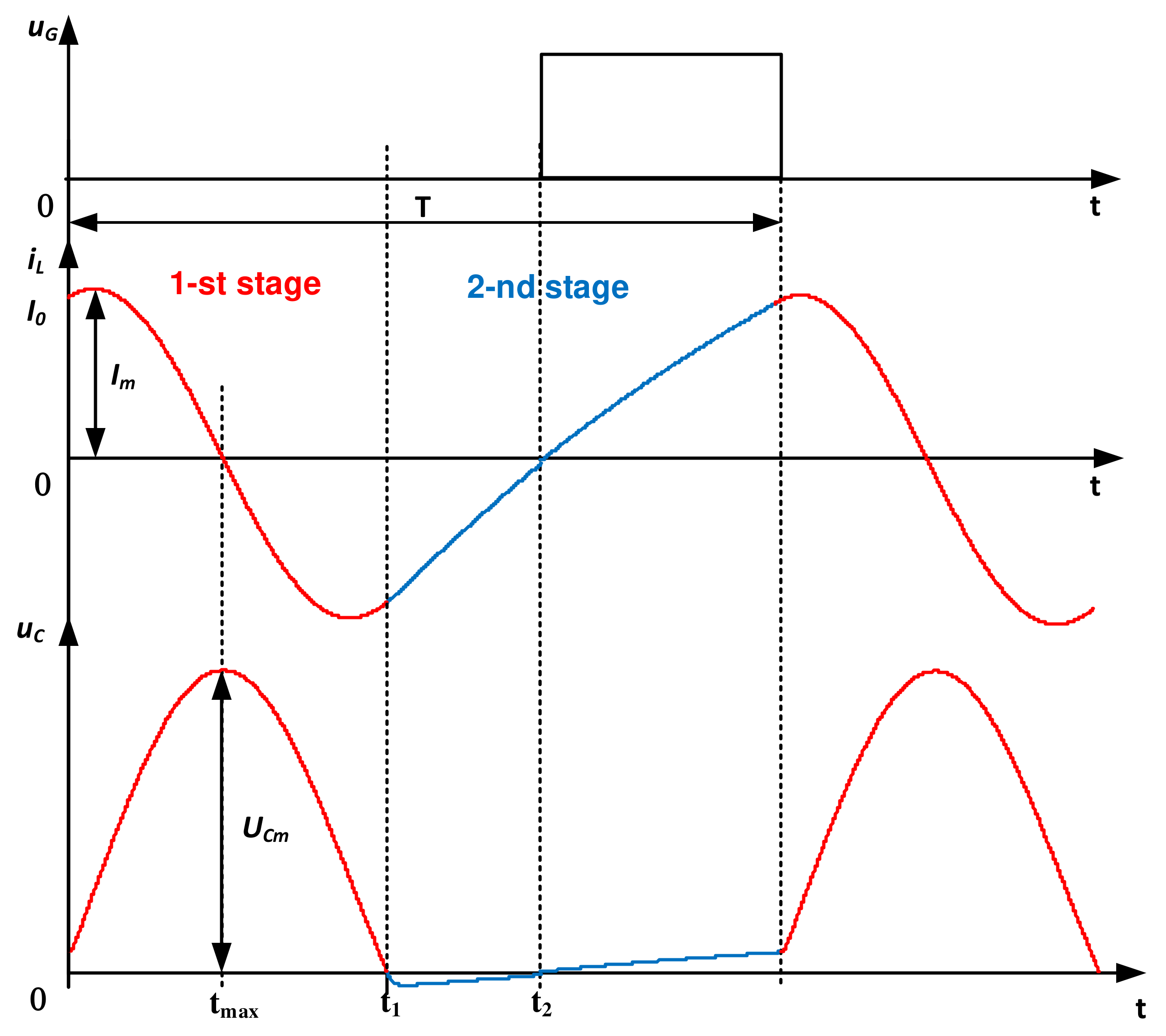
Figure 1 are series single-ended transistor resonant inverter with the direct establishment of the regime (without a transient start-up process), in which a transformer connected to the resonant circuit provides current in a shape close to the sinusoidal to the rectifier and CLC output filter. Single-ended transistor inverters with no transient process can operate in zero voltage switching mode (ZVS), which further improves the energy performance of the converters. On the other hand, the presence of resonant processes leads to the production of significant voltages on the semiconductor switch T (in the range of 3–6 times the input supply voltage
Ud). To control these devices, a method of monitoring the resonant current is used [
23], turning off the transistor T occurs at a certain preset current value. In this way, both the protection and control of the power circuit are combined.
Since the considered converters have a complex structure and it is difficult to describe the electromagnetic processes in the circuit and the creation of basic relations for design, then the use of model-based design is appropriate for determining the circuit elements.
The considered power circuit is composed of two main parts—a resonant inverter and a rectifier with a CLC filter. In this sense, a combined approach will be used in the design to determine the values of the circuit elements—the inverter elements will be designed based on the analysis of the power circuit and the CLC filter elements—through an optimization procedure.
An analysis of the resonant inverter is discussed in [
24,
25]. By turning off the transistor T, a resonant process begins in the series RLC circuit, composed of the equivalent inductance (the resonant
L plus the inductance brought to the primary winding of the transformer
L1), the resonant capacitor
C and the resistance brought to the primary winding—
RR. Due to the presence of a series resonant circuit, the current through the resonant inductance and the capacitor voltage are close to sinusoidal in shape.
Figure 2 shows timing diagrams explaining the action of the resonant inverter.
Solving such a task is related to conducting an analysis of series resonant inverters, which is conducted in detail in the specialized literature [
17,
18,
19,
20,
21], and therefore, the current through the inductance and the voltage of the capacitor is obtained as follows:
where
LR = L + L1,
RR—the total active resistance in the resonant circuit,
I0 is the initial value of the current through the resonant inductance and the initial capacitor voltage
U0 = 0;
and
—respectively—the resonant frequency and attenuation of the series resonant RLC circuit,
—coefficient of variation, analogous to the quality factor
Q [
18,
19,
20],
frequency factor (detuning of the resonant circuit),
ω = 2πf—circular control frequency.
The value of the starting current of the resonant inductance
I0 is determined by the expression [
24,
25]:
where
γ is the duty cycle, representing the ratio of the time when the transistor is turn-on to the period of the control frequency. After substituting the value of the initial current
I0 in (1), we obtain:
To facilitate the further analysis of the scheme, these expressions are presented in a compact form, with the corresponding initial phases:
where
,
—initial phase of the current through the resonant circuit,
,
—initial phase of the voltage on the resonant capacitor.
The considered stage of the operation of the scheme ends with the switching on of the diode D. This happens at the moment
t1 (shown in
Figure 2) and then for an ideal diode it can be considered that its voltage and, accordingly, the voltage of the capacitor becomes equal to zero. In this way, the condition
uC(
t1) = 0 determines the end of this and the beginning of the second stage of the operation of the scheme. Thus, the following equation is obtained, the solution of which is the required quantity
t1:
After conversion, to find the duration of the resonant process in the circuit, the following transcendental equation is solved:
During the operation of the diode, a control pulse is supplied to turn on the transistor, and when its current reaches zero, the conditions are created for turning on the transistor, which repeats the processes in the circuit.
The capacitor voltage reaches its maximum value at the time
tmax when the current through the resonant inductance becomes zero. From the equation of the expression describing the current in this interval, the determination of this moment becomes:
Therefore, the maximum value of the voltage of the capacitor and, accordingly, of the transistor is obtained:
Thus, with the help of the derived expressions, all the parameters necessary for the design of the inverter can be determined. In this sense, the following values of the circuit elements of the inverter part of the converter are defined. In this regard, the following values of the circuit elements were obtained:
Ud = 25 V—input DC supply voltage;
R1 = 0.01 Ω—resistance of the primary winding of the transformer;
L1 = 10 μH—inductance of the primary winding of the transformer;
R2 = 0.01 Ω—transformer secondary winding resistance;
L2 = 10 μH—inductance of the secondary winding of the transformer;
k = 0.9—transformation coefficient, from where we obtain the related parameters: = 9 μH and = 0.009 Ω;
L = 10 μH—resonant inductance;
C = 1 μF—resonant capacitor;
On the other hand, as a result of the accumulated experience from the research of similar schemes [
24,
25], it is possible to determine the initial values of the elements of the circuit of the CLC filter:
R = 25 Ω—load resistance;
L3 = 0.2 mH—filter inductance;
C1 = C2 = 300 μF—filter capacitors.
The power system in
Figure 1 has a changing structure. This change is modeled by the control switching function, which simulates the different states of the converter. It is defined for the serial converter in
Figure 1 as follows:
where
i1 is the current in the primary winding of the transformer,
Ioff = I0—the braking current of the transistor;
uC—the voltage of the resonant capacitor.
Using Kirchhoff’s laws, the systems of Equation (10) are obtained, which model the electromagnetic processes of the series and parallel converter, respectively.
where
control(t) is given in (9), and
i2 are the currents in the primary and secondary windings of the transformer,
i3—current through the filter inductor
L3;
uC1 and
uC2 are the voltages of the filter capacitors
C1 and
C2.
Based on the above systems of equations in Simulink/MATLAB environment, the model of the studied power electronic device is realized.
4. Formulation of an Optimization Task for Design Purposes
In its essence, optimization is an activity to obtain the best result in a certain predefined aspect and with given constraints. In this case, we will strive to realize certain dynamics, which are measured by criterion I (x). This criterion is a number that depends on the choice of some parameter x.
We define the following optimization task—limiting the voltage at the output of the converter
uC1 in transient mode and preventing large pulsations of this voltage in set mode. Limiting the voltage at the output of the converter u
C1 in transient mode and preventing large pulsations of this voltage in set mode is achieved by optimal selection of the following circuit elements: capacitors
C1 and
C2 and inductor
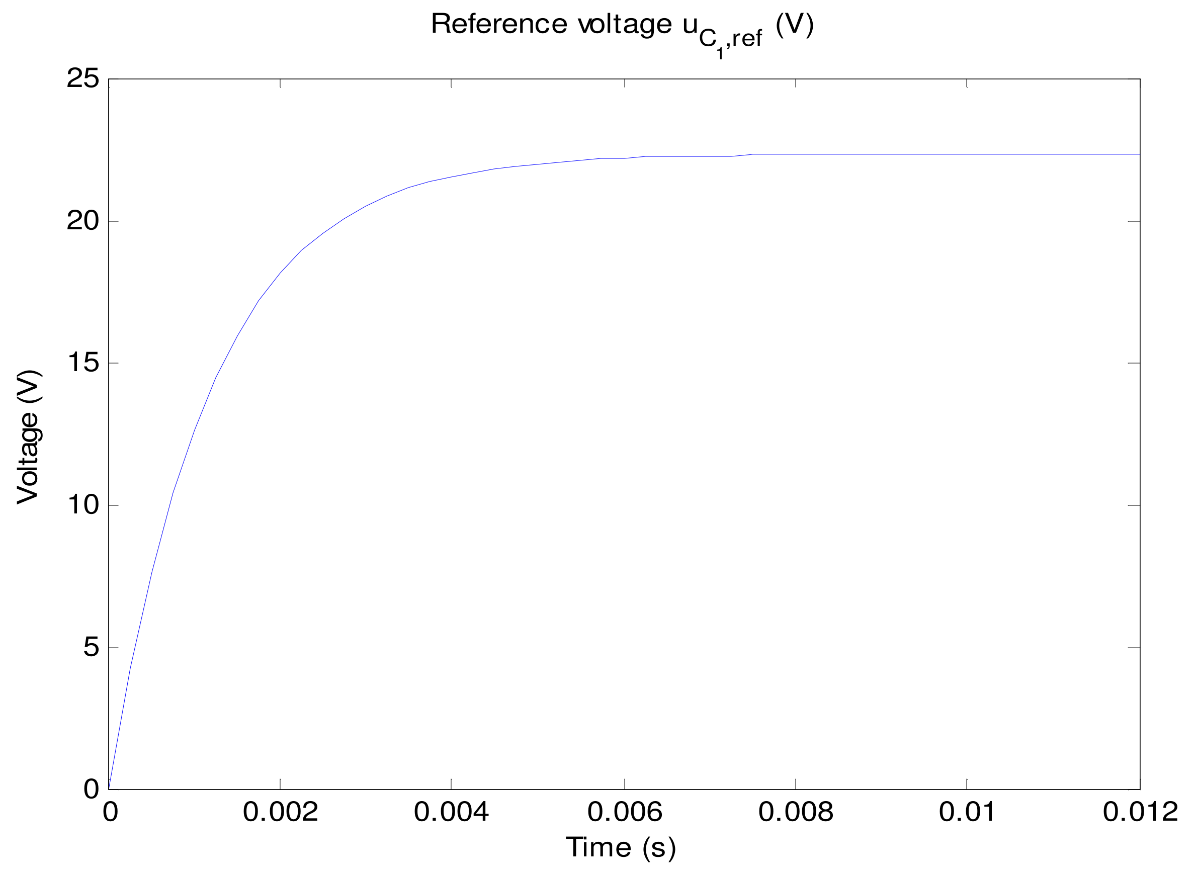
L3. For the realization of this task, a suitable reference trajectory
uC1_ref is chosen, as the one presented in
Figure 3 [
26,
27,
28].
The analytical equation of the reference curve is:
where
T0.95 = 0.0012 is the time-constant of the transient process (i.e.,
T0.95 is the time to reach 95% of the set value of the output voltage of the converter).
The selected trajectory will be used to search for a suitable value of the elements
C1, C2 and
L3, so the difference between the reference form
and the shape of the output voltage
is minimal, and the functionality is minimized [
28,
29,
30]:
This optimization problem is solved for both cases under the following constraints: four constraints of the type of algebraic and differential Equations (9) or (10), which are describing the operation of the converter and six constraints of the type of inequality (13), which define the area of search for the value of the elements
C1,
C2 and
L3:
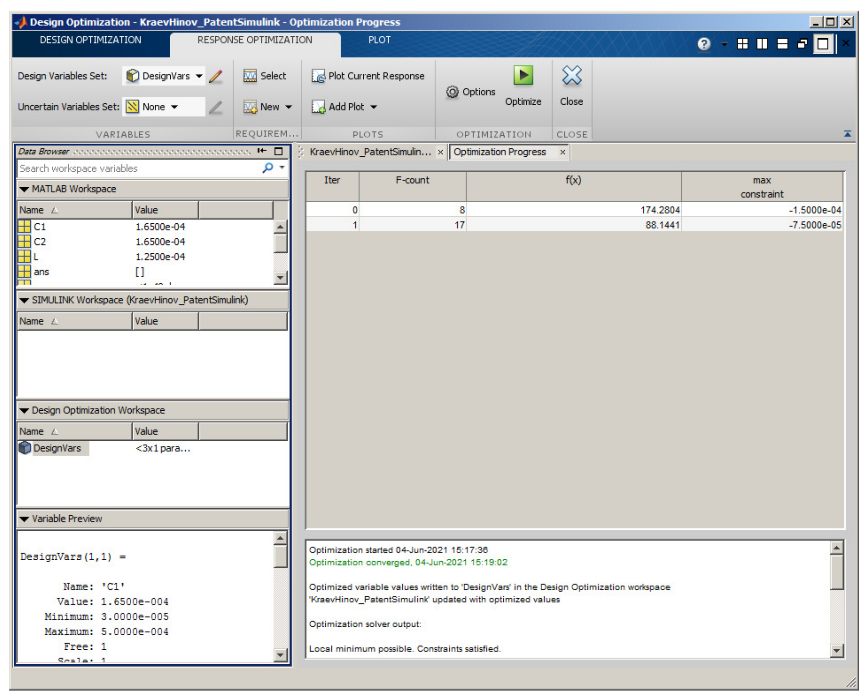
Briefly, the task is recorded as follows [
30,
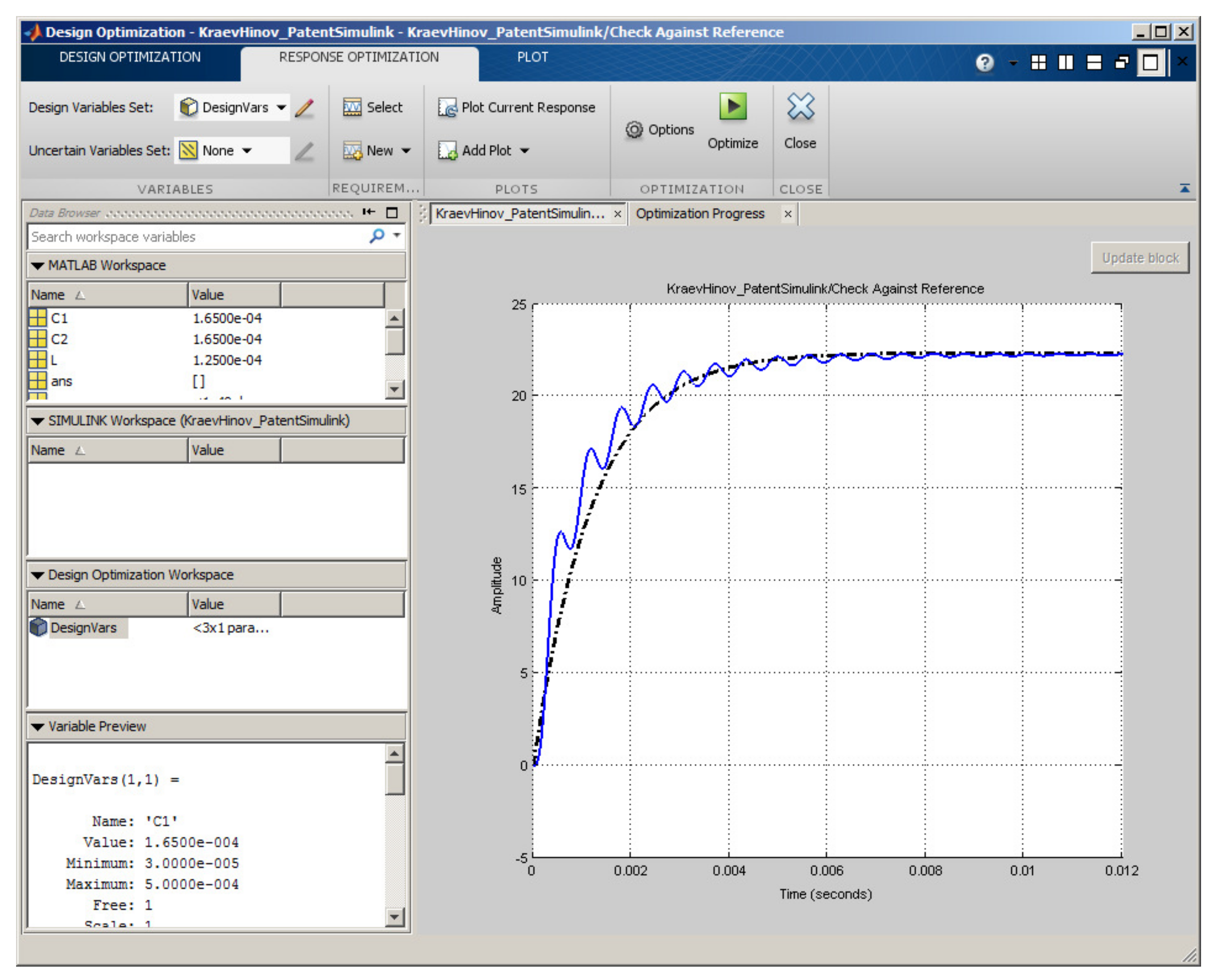
31]. This is an optimization problem that can be solved with a built-in procedure in MATLAB/Simulink (the example uses the following software version—MATLAB R2011b). For this purpose, the MATLAB block “Check Against Reference” is added to the mathematical model. The optimization procedure embedded in the “Check Against Reference” block includes the following steps. The reference trajectory of
Figure 3 is entered. The limits for the
C1.min = C2,min = 30 μF,
C1.max = C2,max = 300 μF and
L3min = 50 μH and
L3max = 1 mH elements are set. Finally, the optimization is started. The process of setting up, executing and obtaining the result of the procedure “Check Against Reference” is shown in
Figure 4 and
Figure 5.
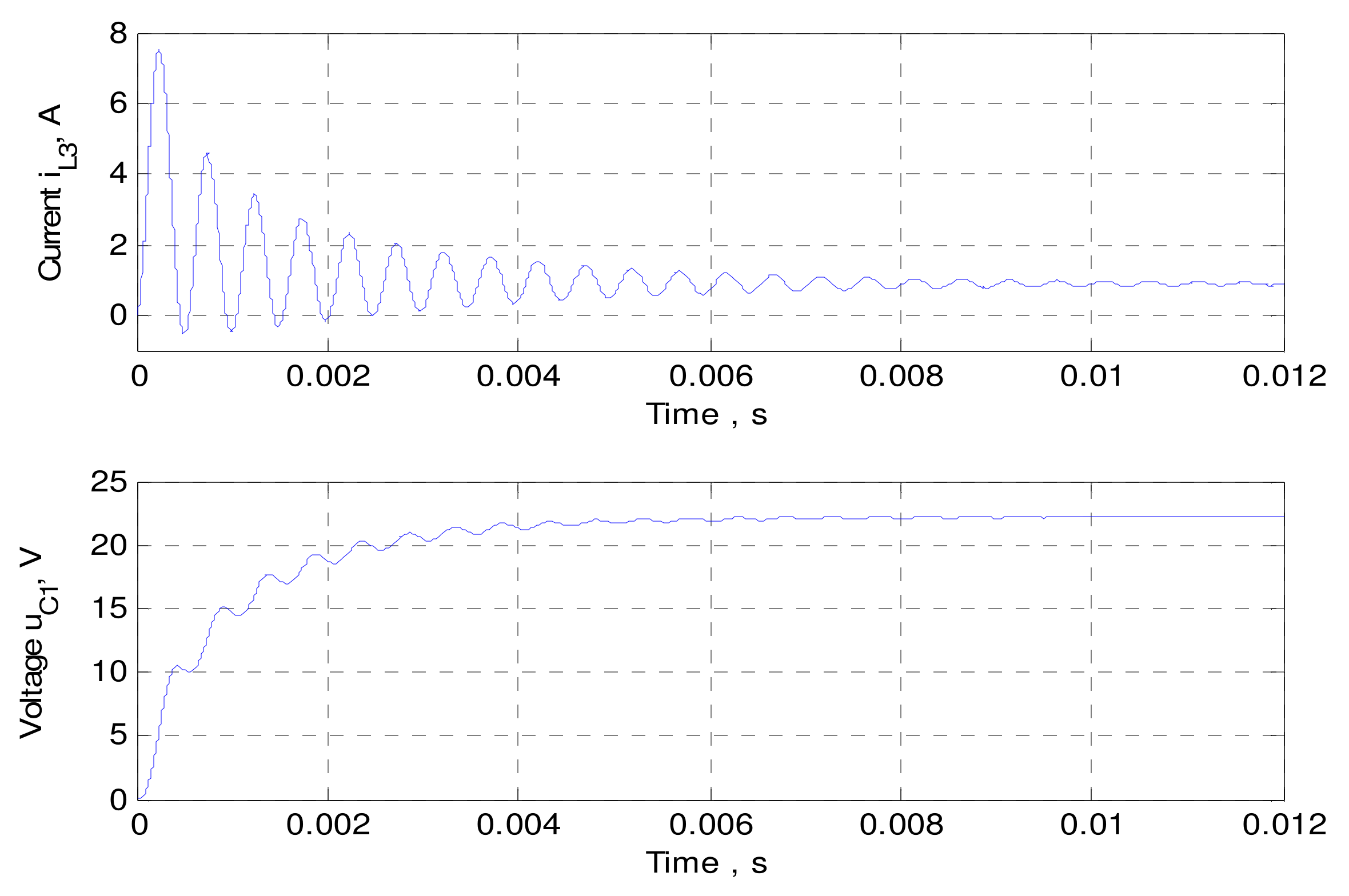
After solving the optimization problem for the series converter, the following optimal values of the filter elements are obtained:
C1 = 165 μF,
C2 = 165 μF and
L3 = 125 μH. After the simulation of the model with these optimal data, the time diagrams from
Figure 6 are obtained.
Figure 6 shows that the desired goals for the voltage shape
uC1 have been achieved, but the current dynamics
iL3 is not good, i.e., there is a sevenfold higher value of the filter inductance current in transient mode and a corresponding slow attenuation of the pulsations in steady mode.
This analysis shows that in order to achieve good dynamics in the output (not a large excess of the current values in the transient modes, compared to the steady mode) it is necessary to supplement and modify the optimization task.
5. Modification of the Optimization Task
To improve the current dynamics through the filter inductor
iL3 will modify the optimization task by adding:
where
iL3max is the maximum allowable value of the current through the filter inductor. In this case, the following value
iL3max = 3A is selected, this is not fulfilled in
Figure 7.
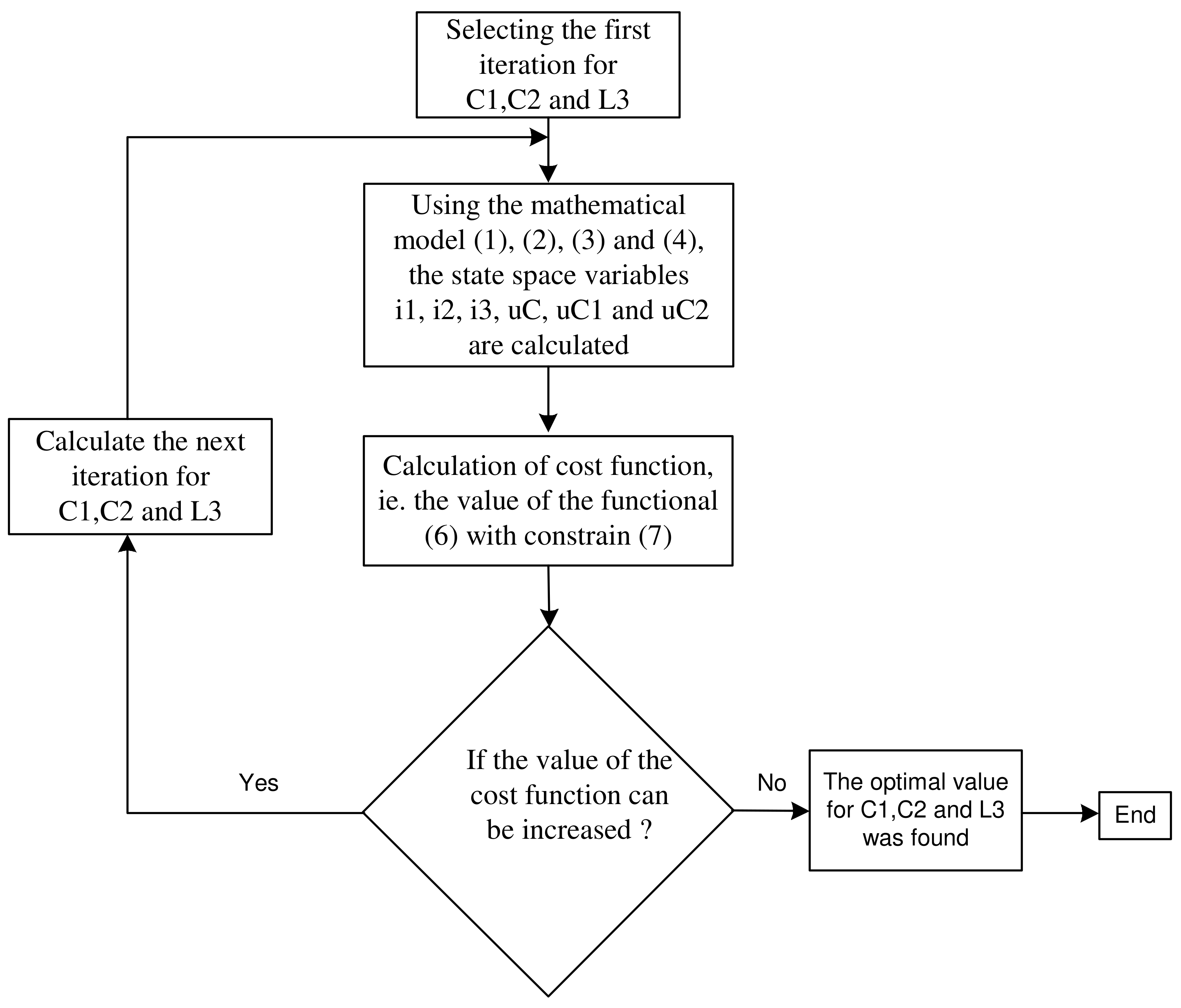
The modified optimization problem, unlike the previous one, cannot be solved using a built-in procedure in MATLAB, because it is not possible to set constraints of the type (14) in the procedure “Check Against Reference”. The reason for this is that in the new optimization problem, a reference trajectory is chosen for one state variable (voltage uC1) and constraints (type of inequality) are introduced for another state variable (current iL3).
This optimization problem was solved in the MATLAB environment, but for this purpose, an author’s program (m-file) was compiled. The author’s program algorithm is shown in
Figure 7.
In the program, the optimization is performed with the “fmincon” command [
31], i.e., [x,Fval] = fmincon(@Opt,x0,[],[],[],[],xlb,xub,@Con,options).
Integral (11) is replaced by the sum of squares of the form
. The constraints (14) are set in “xlb” and “xub” and the initial values are set in “x0”; they are arguments of command “fmincon”. In a special subprogram, the differential Equation (10) is solved with the matrix exponent.
After execution of the optimization procedure for the serial scheme, the following result is obtained,
Figure 8.
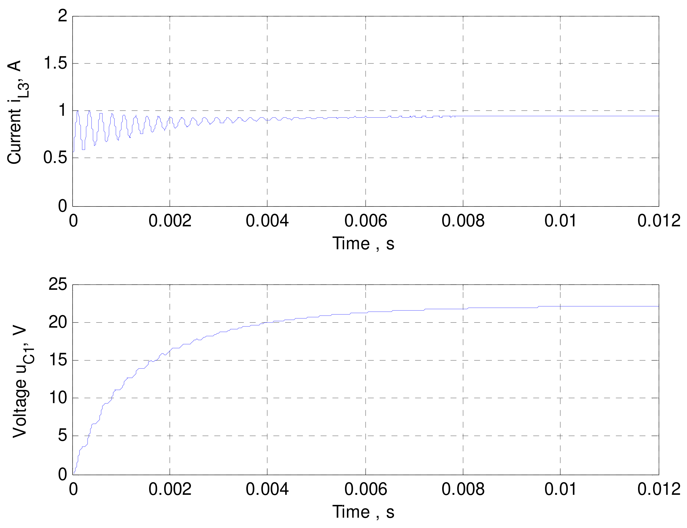
In the end, optimal values for the elements were obtained as follows:
C1 = 30 μF,
L3 = 50 μH and
C2 = 500 μF. With these values, the model of the series DC-DC converter is simulated again and the following time diagrams for current through the filter inductance and the output voltage are obtained, shown in
Figure 9.
Comparing the results for the current obtained by the first optimization and, respectively, with the modified one, shown in
Figure 6 and
Figure 9, it is found that in the modified optimization with good output shape a significant limitation of current deviations through the filter inductance relative to the base case is observed.
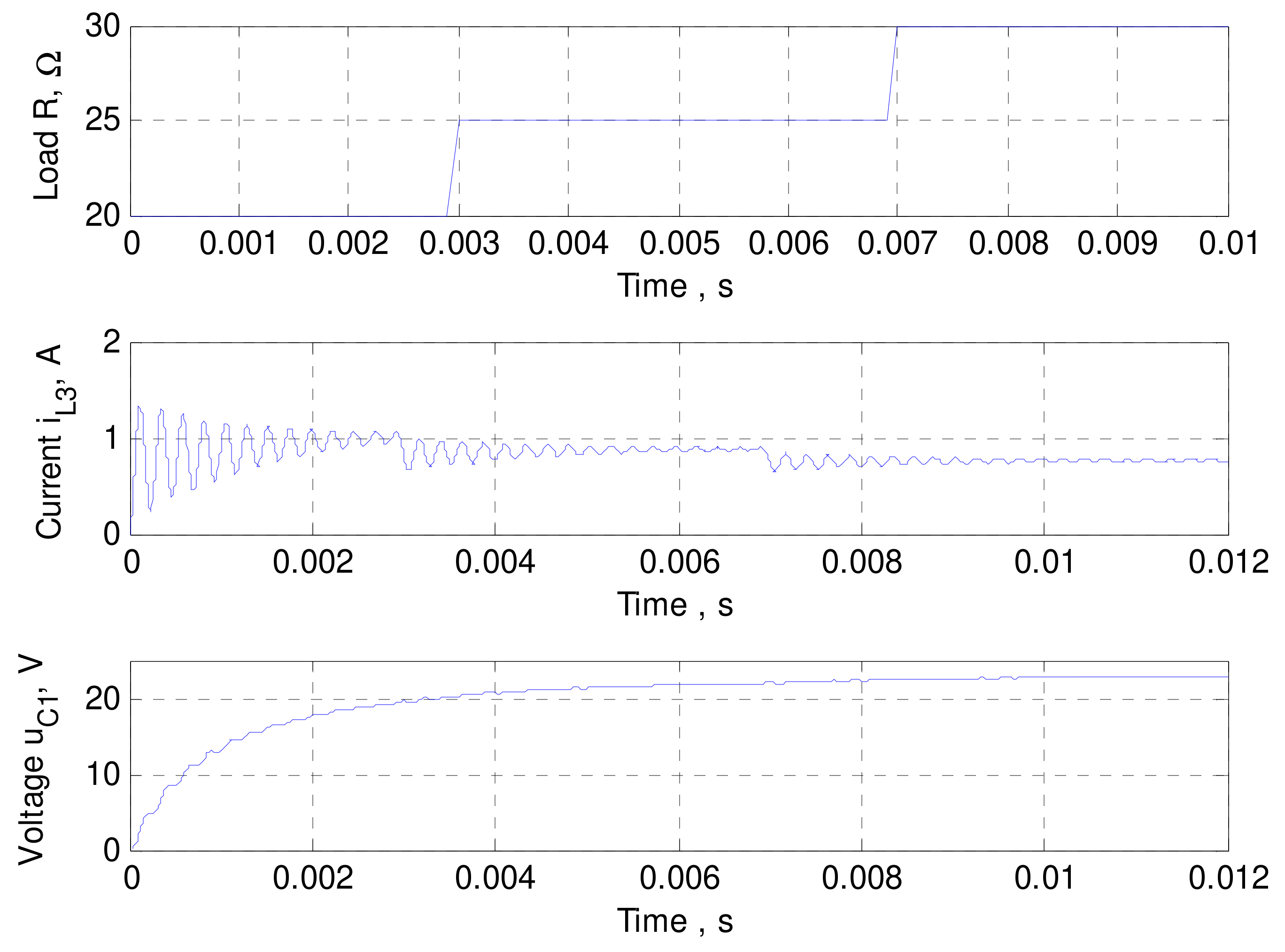
Of interest is the study of the behavior of the converter when the load changes.
Figure 10 shows the results of numerical experiments carried out with the optimized DC-DC converter at different values of load resistance. From the diagrams, it is found that the circuit behaves stably, with the current ripples being smaller than at the nominal value of the load resistance.
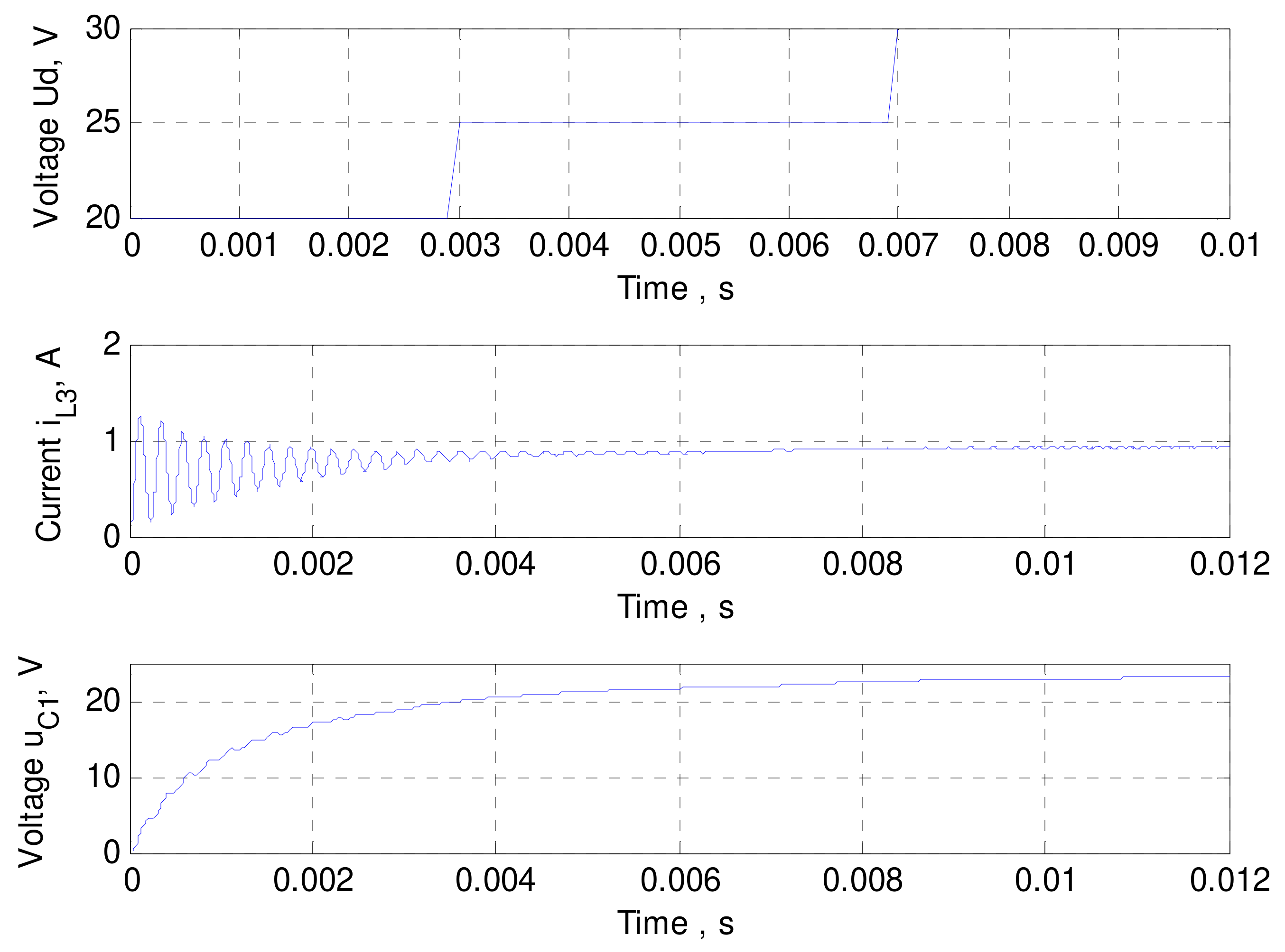
Figure 11 shows the results of numerical experiments carried out with the optimized DC-DC converter when changing the input voltage
Ud.
From the graphs, it is found that even with the double increase in the load resistance, the operation of the DC/DC converter is stable, in this case, the current ripples increase, but despite this, the limitation set during the optimization regarding the output current is not violated. On the other hand, despite the drastic change in the load compared to its nominal value, the aperiodic nature of the transient process regarding the load voltage is preserved, which was also the main condition when conducting the optimization procedure.


