1. Introduction
Power supply modules are connected in parallel to provide the most reliable and efficient power system. Connecting converters in parallel is beneficial in terms of modularity enhancement, larger power requirements, and design flexibility. The above-mentioned benefits can only be achieved from a parallel-connected design if the load current sharing between the converters is distributed evenly. Although parallel connections of the power supply module are one of the most operational methods, they require severe surplus considerations, i.e., in terms of a current balancing controller to sustain the line current, the input current distortion, and the current stress between the modules.
Power is shared between the parallel-connected converters in such a way as to attain a cost-effective design and to shrink the system size and weight. Reliability of the system can also be increased through such an approach to implement the fault tolerance redundancy. Each module has supreme efficiency because it operates at its optimized power level. Power converters were initially arranged in parallel design in an inverter uninterruptible power system UPS [
1]. After that, different topologies and their controller were reported in [
2,
3,
4,
5,
6]. All these proposed schemes show that system control, maintenance and protection depend upon the configuration of the systems, keeping the modules identical. Converter modules in [
2,
3,
4,
5] are explored based on system reliability, performance, and ripple reduction. Guaranteeing the maximum power delivery and means of isolation and failure detection was proposed in [
6].
For DC/DC parallel-connected converters, different control techniques are formerly presented in [
7,
8,
9,
10,
11] for controlling the load current sharing. Amongst these controllers, that of [
7,
8] is the most effective and easy to implement. More details about connecting modules in parallel are reported in [
7,
12,
13]. Regarding the reliability and capacity of the power systems, the parallel-connected modules in AC/DC converters provide better results as compared to DC/DC converters. These parallel-connected converter arrangements are also obliged, for eliminating harmonics from the input line current and for power factor correction, to have rectifiers as the most important part in power systems. Converters connected in parallel along with the current sharing controller are presented in [
14].
One of the main hindrances in the parallel-connected power converters discussed above is circulating currents that flow from one device to the other, which is sometimes very dangerous for the whole setup. As each converter is separately designed, connecting multiple of them in parallel will result in a problem of circulating currents [
6,
15,
16]. Circulating currents in such setups are responsible for unequal load sharing between the converters, which degrades the whole system’s efficiency. Different techniques are adopted for the mitigation of these unwanted circulating currents. The use of isolation transformers in an AC grid are proposed in [
17,
18], which is the most helpful method, but the only problem in this technique is an expensive setup. A synchronized control scheme [
15,
18,
19] is proposed in which the parallel converters were treated as a single converter to deal with circulating currents. This scheme adds some extra stress to the input capacitive filters, and adding a parallel setup is also an issue because it makes it a more complex control system.
For parallel-connected modules, two types of control architectures are followed, i.e., either a centralized or decentralized control. The concept behind the centralized control system is similar to a unified single-handed control whose drawback is the performance and reliability degradation in terms of a single point failure [
20,
21]. A decentralized control system’s main hindrance is the lack of communication between parallel-connected converters, resulting in unequal current sharing between the parallel-connected modules [
22,
23]. For parallel-connected converters having separate voltage and current control loops, a droop-based PI controller is used [
24]. It is evident that circulating current control has an inverse relation with the value of droop resistance, i.e., for a small value of droop resistance, a high value of circulating current is obtained and vice versa. An increase in the value of droop resistance to reduce circulating current results in unequal current sharing and voltage regulation. It causes the power electronics converter circuit to have a low power factor for the overall system.
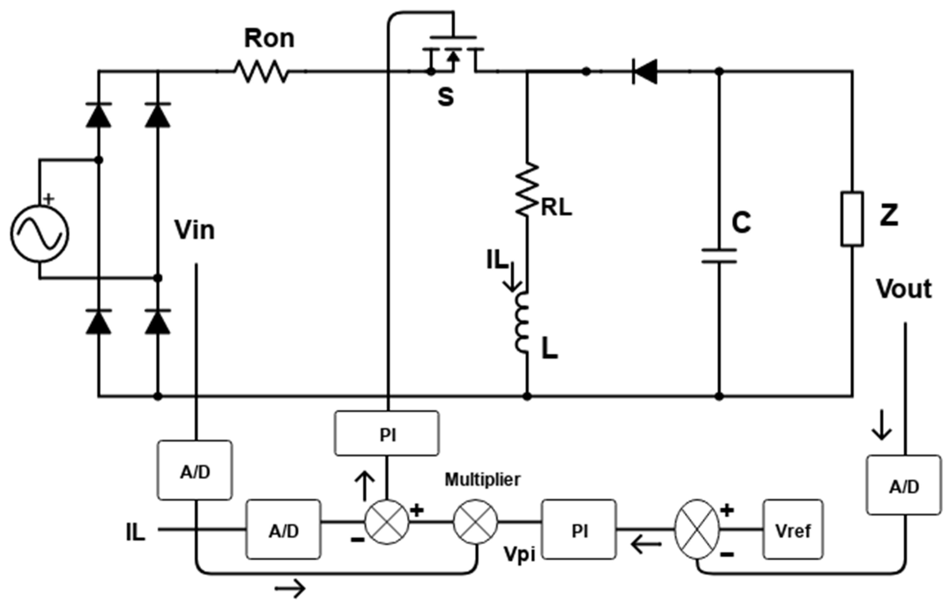
With the development of digital signal processors (DSPs), and other digital chips, more multifaceted and advanced algorithms can be part of any control system, which is a crucial reason for favoring digital control over analog. Apart from this, there are a few other forms of dynamics that embrace truncated environmental distinction vulnerability, the developed performance of the digital control, programmability, and malleability. Due to all these advantages of digital control, researchers have started working on discovering digital controls for power factor correctors (PFCs). The scholars primarily use the average inductor current mode control (AICMC) technique for executing digital control. However, digital management also has few constraints in terms of converter switching frequency speed, which is associated with the DSP speed. Therefore, considering this fact, a supervisory controller is proposed in this paper for digital feed-forward control of buck-boost converters connected in parallel. This digital supervisory control will help bring the power factor to unity and circulating currents to almost zero.
The proposed control scheme is based on the mathematical modeling of a buck-boost converter to provide a digital control technique using the converters’ equations. The novelty of this work is that it provides the calculation of the unity power factor duty cycle and a control technique that can ensure harmonic reduction and voltage regulation at the consumer end. The proposed control scheme works perfectly in terms of the parallel connection of multiple modules. The load current sharing between the modules with low harmonic content is achieved successfully with the help of this technique. This work also provides desirable control over the circulating currents and eliminates these harmonics from the system. This technique is compared with a conventional control method, i.e., AICMC, to demonstrate the proposed control scheme’s supremacy in terms of circulating current control and elimination of harmonics from the line current. Reduction in the circulating currents of the parallel-connected power system, elimination of harmonics, and the high power factor of the system are the proposed control scheme’s basic findings. Commonly used normal speed processors are enough to perform all the instruction sets of the proposed control scheme.
In this paper,
Section 2 discusses the earlier-stage digital PFC control implementation problems. A brief overview of different operating modes of power converters is provided in
Section 3. Digital buck-boost converter PFC feed-forward control is derived in
Section 4. A supervisory controller containing feed-forward control for a parallel-connected buck-boost converter PFC is highlighted in
Section 5.
Section 6 of this article presents the optimization technique for the purpose of improvement in the proposed control scheme.
Section 7 presents a brief discussion about the types of circulating currents. Simulation results are presented in
Section 8, while a hybrid digital validation of this scheme is performed in
Section 9. The conclusion is presented in
Section 10.
2. Earlier-Stage Digital Control PFC Implementation Problems
Due to the processing time and sampling delay in digital control systems, there is a restriction on the switching frequency. As debated above, AICMC is a frequently used technique for analog control, as shown in
Figure 1. This AICMC technique is also used for digital control in [
25,
26,
27,
28]. For improving the power factor of a system, the inductor current
iL is multiplied by the rectified input voltage
Vrec, and then it is pushed to follow the reference current
iref. In the AICMC technique,
iL and
iref are used as feedback currents and, from their difference, the duty cycles for the switch are calculated by DSP for every switching cycle
Ts. The whole process of AICMC encompasses the following stages: voltage error and sampling stage; PI voltage regulator stage; attaining inductor reference current and current error; PI current regulator stage; and, at the end, duty cycle generation stage for the switch. In addition, the PWM stage is also used for obtaining duty cycles for PFC implementation. This, all of these processes run simultaneously, and they should be completed in each cycle
ton time to achieve power factor correction. In analog implementation, there is no restraint, but in digital control, it is correlated with the processor speed, where the switching frequency is limited in some cases. Thus, this is the main hindrance to a digital control scheme.
In reference [
29], a control method is proposed to reduce the computational speed of the DSP. In this reference, the duty cycle values for the converter switches are updated once in whole switching cycles. They are applied several times without editing to reduce the computational burden of the DSP. Boost converters are used as a power converter in [
29], which results in harmonics in line currents. Duty cycle calculation per switching cycle is also minimized to escalate the switching cycle and diminish the calculating time. However, due to this, harmonics are created in the system, resulting in low PFC. Another method is presented in [
30] with two parallel control loops, i.e., open and closed loops. The open loop was responsible for determining the duty cycle values with the help of output and input voltages, and the closed loop provided the second duty cycle component. Nonetheless, the same issue of the duty cycle calculation in each cycle was a concern. A predictive control scheme was applied in [
31] for predicting the duty cycle values for the converter switches. Duty cycle values for the next cycle were predicted with the help of input and output voltages and the constant duty cycle values. Significant calculations in each process were again an issue here.
From the above discussion, all the complications can be classified into three main hindrances of digital control over analog control. In digital control operation, switching frequency is the first hindrance, limited due to the processing and calculation time. The second disadvantage is the speed of a processor. A processor should be faster even in comparatively slow switching frequency operations of the PFC. Although DSP speed has a linear relationship with the switching speed, for a high-speed switching frequency, using a high-speed DSP is subjected to the high-cost problem. If a high-speed DSP is used despite its high cost, there is still a problem in the switching frequency level, which is far lower than that of analog control implementation; this is the third and the most important disadvantage.
A new digital control strategy for buck-boost PFC is used in this paper to present solutions for all the above problems. The proposed control scheme can provide power factor correction with a wide range of input supply voltages. A control scheme is presented for both conduction modes, i.e., CCM and DCM of a buck-boost converter. It can also deal with circulating currents between parallel setups.
3. An Overview of CCM and DCM
In continuous conduction mode (CCM) of a converter, the current inside the inductor
iL(
tK) never drops to zero. The general waveform of the inductor current
iL(
tK) is shown in
Figure 2a. For the first interval, the inductor current increases when the MOSFET is ON, while for the OFF state of the MOSFET, in the second interval, the inductor current decreases. The converter’s discontinuous conduction mode (DCM) occurs when the switching ripple is larger in the inductor current for a light load at the output end. The DCM mainly occurs in converters with low loads/no loads, while some converters are also specifically designed to be operated in DCM for each type of load. The inductor current in the DCM, shown in
Figure 2b, increases when the MOSFET switch is ON, while for the second interval, when the MOSFET switch is OFF, the inductor current gradually decreases to zero. For a pure PFC AC/DC converter, the line current will be in phase with the line voltage for a unity power factor. Thus, the inductor current
iL(
tK) can be found as:
where
Vr(
tK) represents the rectified input voltage with
VM as peak rectified voltage and
Re represents an emulated resistance. For an AC/DC buck-boost converter operating in CCM mode, we can write:
So, the emulated resistance can be written as:
V represents the constant output voltage of the converter. Thus, for the CCM mode of the converter, we can conclude that:
while for DCM mode of the converter:
Therefore, we can say that the converter operates in CCM if
Vr(
tK) approaches
VM, and the converter operates in DCM if
Vr(
tK) approaches zero; we can define the intervals
d1k,
d2k, and
d3k as 1st, 2nd, and 3rd phases during a single PWM period, respectively. These intervals can be further used for expressing the modes of the converter as:
4. Feed-Forward Algorithm for Buck-Boost Converter
Below, two assumptions are given for deriving a feed-forward control algorithm for a buck-boost converter:
Buck-boost converter operation is either in continuous conduction mode (CCM) or discontinuous conduction mode (DCM).
During one switching cycle, input voltage Vin is constant because the switching frequency is greater than the line frequency.
Based on a single switch, the buck-boost converter operation is distributed into two primary states, i.e., the ON-State and the OFF-State. In these states, keeping the above two assumptions in mind, the inductor voltage is given by:
Equations (8) and (9) represent the inductor voltage for ON-State and OFF-State of the switch, respectively.
According to the above supposition that the switching frequency is much higher than the line frequency, Equation (8) can be replaced by Equation (10):
For continuous conduction mode (CCM), Equation (9) becomes:
For discontinuous conduction mode (DCM), Equation (9) becomes:
whereas:
The inductor current at instant
tk + dk ·Ts and
tk + 1 from the above equations are given by:
Rearranging the above equations, we obtain:
As argued above, in AICMC, for power factor correction perseverance, the output voltage is related to the reference voltage and then passed through the PI voltage regulator to track the reference voltage
Vref. At the same time, the inductor current is enforced to follow the reference current
iref(
k), which is acquired from voltage PI regulator and is proportional to the rectified input voltage, as shown in
Figure 3. Thus, we can perform the following substitutions:
For CCM, considering Equations (19)–(22), the value of the duty cycle is attained for the switching period
k from Equation (17) as:
For DCM, considering Equations (19)–(22), the duty cycle value from Equation (18) is attained and given by:
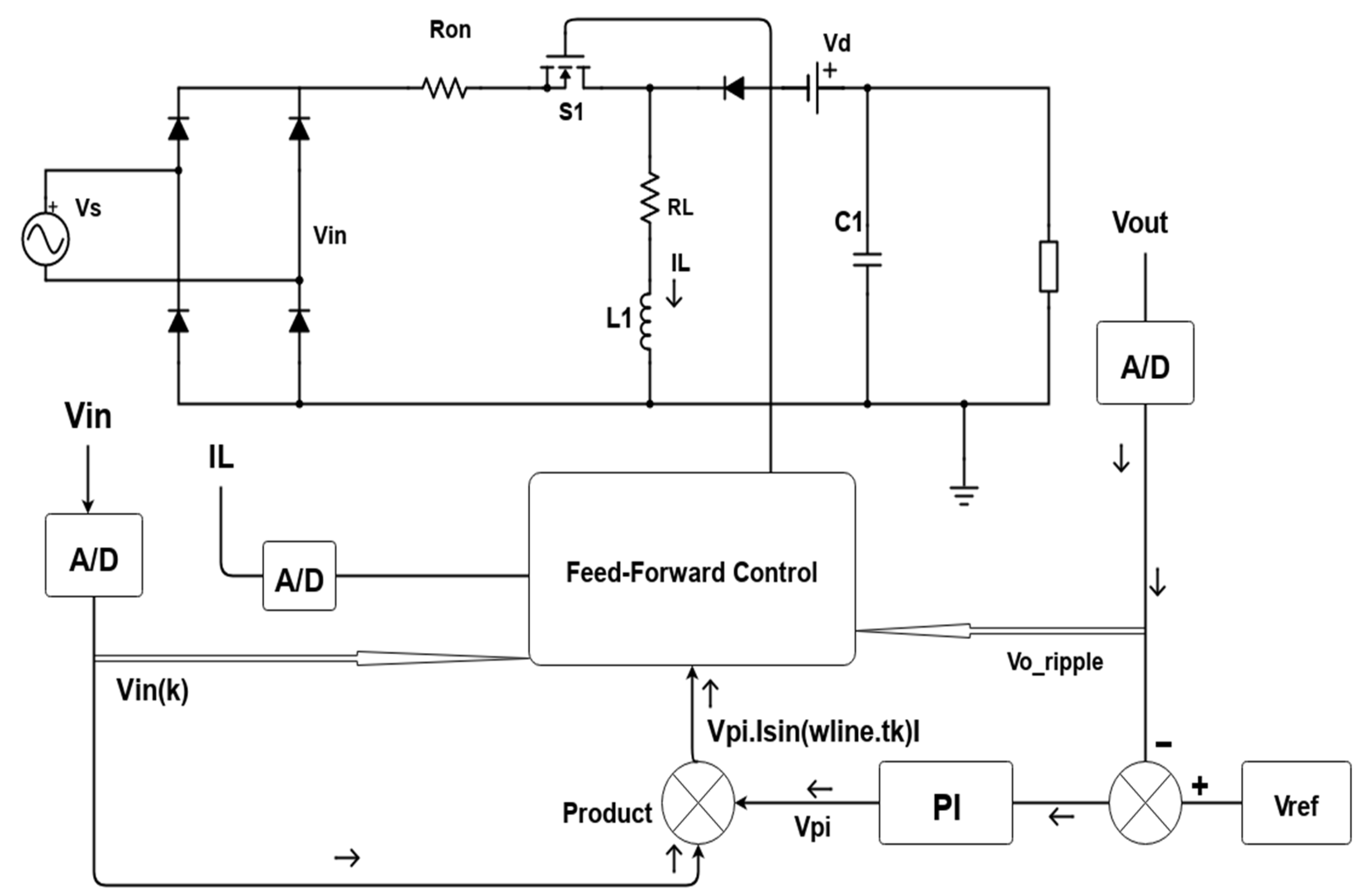
Equations (23) and (24) show the feed-forward control for the buck-boost PFC to obtain duty cycle values. Referring to the performance competencies, a detailed topology of the buck-boost converter is shown in
Figure 4 to improve the performance in obtaining duty cycle values. Switching resistance
Ron, inductor resistance
RL, diode voltage drops
Vd, and the ripple at output voltage
vo_ripple are considered in the calculations, and their results are observed. Therefore, referring to the most precise model in
Figure 4, the duty cycle calculation is given by Equation (25) for CCM and Equation (26) for DCM:
Equations (25) and (26) are the required feed-forward control for buck-boost PFC operating in CCM and DCM, respectively. Output voltage ripple
vo_ripple and
vin(
k) can be calculated by:
From Equations (25) and (26), it is evident that the instantaneous current
iL(
tk) and
iL(
tk + 1) are forced to track the reference current
iref. This
iL(
tk) is also accountable for finding the inductor resistance voltage drop. The block diagram of the digital control algorithm for the buck-boost PFC is shown in
Figure 5. It primarily consists of two control loops: the voltage control loop (outer loop) and the current control loop (inner loop). Feedback signals in this feedforward control are
vo and
vin.
Reference current iref is obtained from the voltage loop, where the output voltage is compared with the reference voltage and then passed through a voltage PI regulator. For obtaining the sinusoidal behavior, it is multiplied by sin(wline ·tk) from the rectified version of input supply voltage. The feed-forward control block yields gate signals for the unity power factor to the switch.
5. Feed-Forward Algorithm for N-Parallel-Connected Buck-Boost Converter PFCs
For the derivation of the power factor correction, inductance is needed. Increasing the inductor value for a high power rating will also increase the dimensions and stress. To abolish this stress, a parallel connection of PFCs is used to stake the stress among them. The load current is shared between each PFC depending upon their capability and their remoteness from the load. Parallel connection also magnifies the system’s energy storing capacity, which supports the assessment of the outer power capabilities. PFCs connected in parallel offer the same output power level for small inductor values compared with the conventional single PFC.
The feed-forward control for
N parallel-connected buck-boost PFCs, shown in
Figure 6, consists of source voltage
vin, switching period
Ts, inductance
L, and output voltage
vo. In the feedback loop, the inductor current is also added in the form of
Is(
k), which is the sum of the inductor currents of
N converters connected in parallel. Both assumptions remain the same, i.e., parallel-connected PFCs are functioning in continuous conduction mode (CCM) or discontinuous conduction mode (DCM), and their switching frequency is much higher than the line frequency, so the input voltage during one cycle is taken to be constant. The control considered here is feed-forward, while the current behavior of the inductor is shown by the present switching cycle [
32,
33].
Taking the assumption into account that
L = L1 + L2 + … LN, summing all the inductor current will result in the source current
Is(
k) [
34], i.e.,
For
Ts, the source current
Is(
k) in case of parallel-connected buck-boost PFC is given by:
Considering Equations (25) and (26) and
Is(
k) from Equation (30), feed-forward control is derived for
N parallel-connected buck-boost PFCs operating in CCM and DCM [
35], respectively, by Equations (31) and (33):
where
Kc is given by:
and:
This technique helps obtain duty cycle values in individual switching prompts and also excludes the errors from the system that arise in the preceding switching cycle.
6. Feed-Forward Control Technique Improvement by Optimization Technique
The optimization of the value of L from Equations (25) and (26) is performed to improve the effectiveness of the proposed control scheme because the parameter L has a significant direct impact on the value of total harmonic distortion (THD). The parameter L is part of the duty cycle calculation equations for both CCM and DCM modes of a converter, so optimizing this parameter value can improve the power factor almost to unity. THD of the line current has an inverse relationship with the system’s power factor. The question arises here: why optimize the value of L only, as we have other parameters in these equations? The answer to this question is that L has a dominant effect over other parameters. The effects of changes in other parameters on THD can be compensated by adjusting this parameter L.
Therefore, for optimizing this parameter
L, the line current’s THD is considered an objective function. The inductance
L is considered a non-linear function of this THD, and it can be written as:
The value of parameter
L is optimized using Equation (34) to reduce the value of THD. The optimized value of THD will be slightly different than the physical value of
L. The secant approximation of Equation (34) is expressed in Equation (35) to show the gradient of the function
, i.e.,
whereas the updated value of this parameter
L can be achieved by Equation (36):
The value of the gradient is obtained from Equation (35). Equation (36) is iteratively implemented until the objective function is minimized to achieve a higher power factor for the system. This optimization can be implemented in the control technique by sensing the inductor current value, as shown in
Figure 7. This value of inductor current is saved in the processor to analyze its harmonic component with the help of fast Fourier transform (FFT). The DSP uses Equation (36) to optimize parameter
L to
L*. This optimization method is not always part of the control system as it depends upon the DSP to decide whether it is needed.
7. Circulating Currents in the Proposed Scheme
There are two main types of circulating currents in power converter circuits, depending upon their topologies, i.e., if the converters are connected in interleaved topology, there are common-mode circulating currents (CMCCs), whereas if the two converters are connected in parallel, then the circulating currents will be differential-mode circulating currents (DMCC). In this article, as the case of two converters connecting in parallel is the focus, we deal mainly with DMCCs. A brief description of both types of converters’ circulating current is presented.
- (a)
Common-Mode Circulating Currents (CMCCs)
Common-mode circulating currents (CMCCs) refer to the types of circulating current that exist in the interleaved topology of the converters. CMCC is the difference between the inductor currents of the two legs of interleaved topology [
36], i.e.,
- (b)
Differential-Mode Circulating Currents (DMCCs)
The differential-mode circulating currents (DMCCs) are the main part of the parallel-connected converter system, which is the main focus of this article. DMCCs are the difference between the inductor currents of the first leg of each parallel-connected module, i.e.,
Here,
δx represents the distribution factor, and its value should be between 0 and 1, i.e., (
0 ≤ δx ≥ 1). This distribution factor is given by:
where
Px represents the power of that individual converter, and
Ptotal represents the total power of the parallel-connected converter module system.
The DMCCs are mainly due to the difference in the switching timings of the parallel-connected converters. This difference in the switching timings will also lead to the unbalanced load current sharing between the parallel-connected modules. Focusing on the problems discussed above, a centralized control system is presented. The outer control loop is for output voltage control and provides the reference current to the inner/current control loop. This reference current coming out from the voltage control loop is multiplied by the distribution factor
δx to provide the DMCC controller along with the feed-forward controller, as shown in
Figure 6.
8. Simulation Results
The proposed scheme was verified in MATLAB/Simulink with power system parameters shown in
Table 1. As an example, three buck-boost converters were connected in parallel, which initially took the values of the inductors as being identical to each other i.e.,
L1 = L2 = L3 = 0.5 mH; then, simulations were undertaken for different values of inductors i.e.,
L1 = 5mH,
L2 = 0.5 mH, and
L3 = 0.05 mH. The input voltage was taken as 300 V, switching frequency was maintained at 10 kHz, and line frequency was 50 Hz. The simulations were performed for variant loads to validate our proposed scheme. The results plainly indicate that harmonics in the current waveforms are reduced, which lowers the THD value. The power factor was also improved. It also indicates that when inductors are identical, then load current is correspondingly shared between the converters. In contrast, when inductors have different values, then load current will be shared according to their capabilities. All the results are shown below in
Figure 8,
Figure 9,
Figure 10,
Figure 11,
Figure 12,
Figure 13,
Figure 14,
Figure 15,
Figure 16,
Figure 17,
Figure 18,
Figure 19,
Figure 20 and
Figure 21.
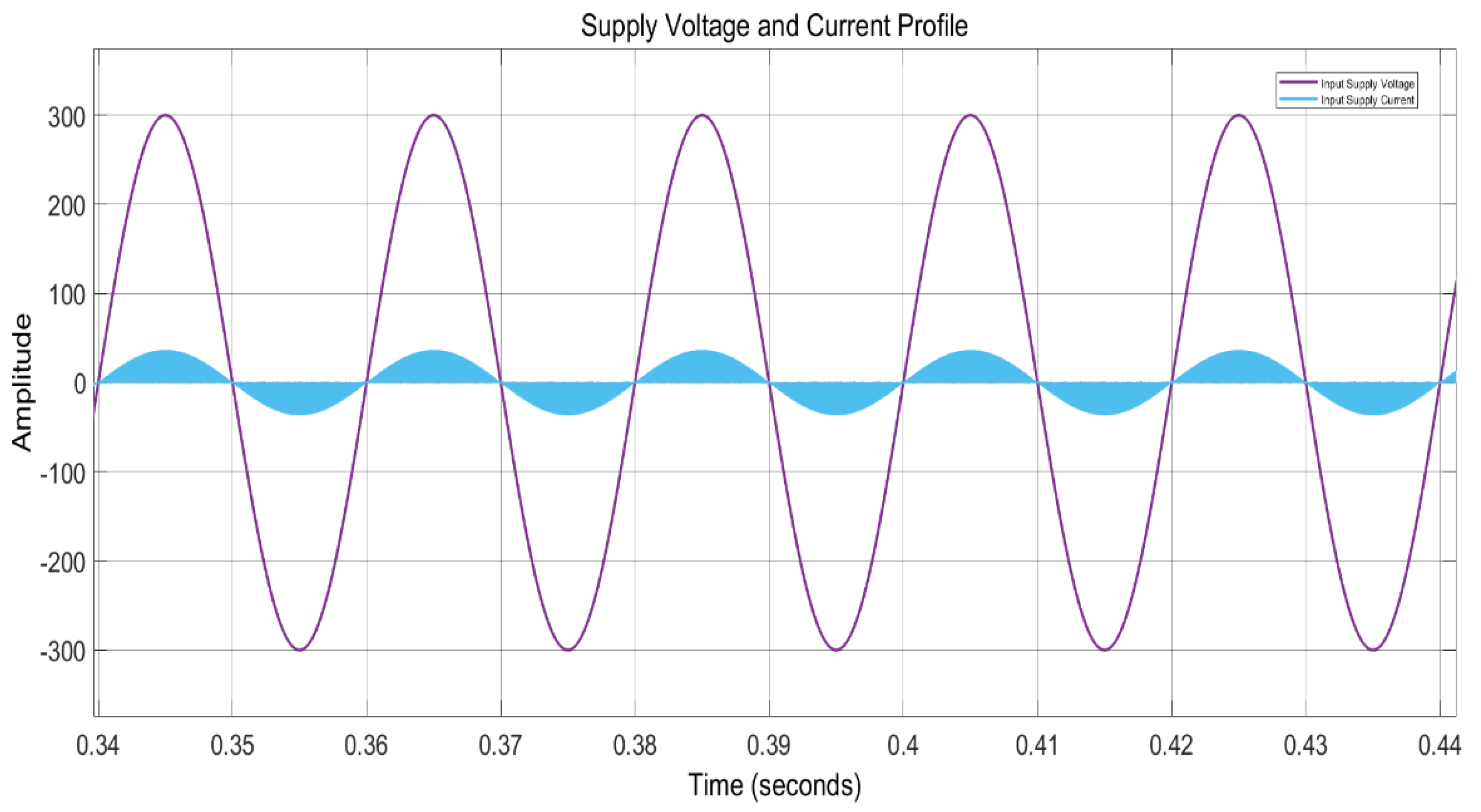
Input voltage and currents are sinusoidal, as shown in
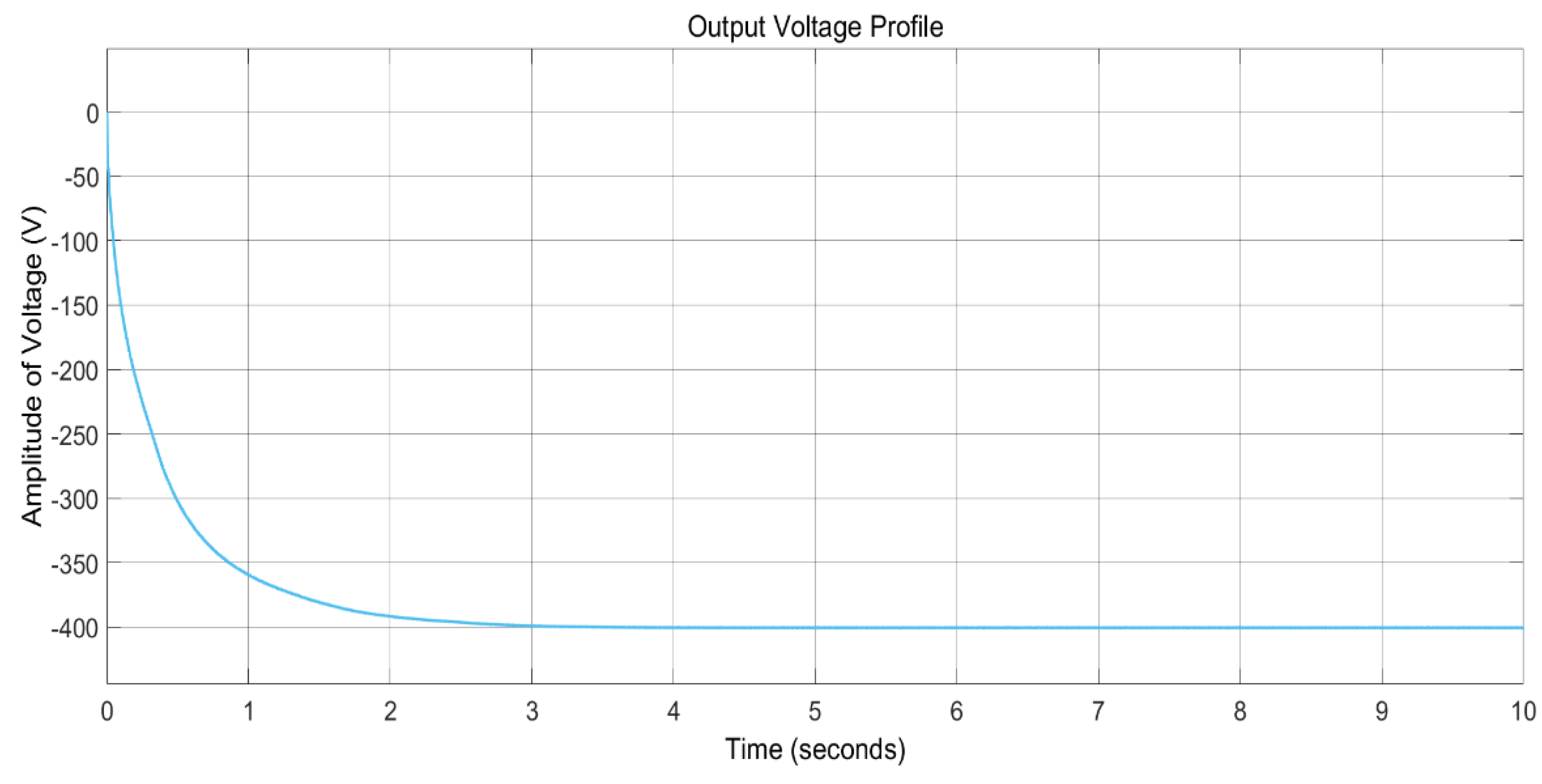
Figure 8. The reference voltage given is 400 V, so the output voltage shown in
Figure 9 is retained at 400 V using the PI voltage regulator as an outer voltage control loop. This outer loop is followed by the supervisory controller loop comprising the feed-forward control derived for both CCM and DCM. Output from the PI voltage regulator is taken as a reference inductor current by the supervisory controller (inner loop). Due to this supervisory controller, the inductor current will tend to track the phase of the reference inductor current provided by the outer loop to enhance the line current in phase with an input voltage, as shown in
Figure 8.
In both cases, the output voltage is enhanced according to the load variations, and the ripple from the output DC voltage is clamped by sampling it on each zero interval. For both cases, the output voltage is sustained at 400 V delivered to a joint load at the output end. The output currents when the inductors have the same values are shown in
Figure 10. Gate signals from the supervisory current controller given to both the switches, and the power factor, are shown in
Figure 11 and
Figure 12. The power factor is retained around 0.997 with THD of 4.42%. Inductor currents when all the inductors have identical values are shown in
Figure 13, which shows that the output current is similarly shared between them, and the inductor current with different inductor values is shown in
Figure 14.
The total harmonic distortion graph of whole system is given in
Figure 15, which offers the minimum value of THD for the system. In our specific case, the distortion power factor is the focus. A system with switching power converters refers to a non-linear system, so the power factor correction performed in this case will result in an improvement in the distortion factor. The power factor is obtained by the product of both the displacement and distortion factor, i.e.,
For the resistive load, the cosine of the angle between voltage and current is zero, while for the value of THD of 4.42, the power factor corresponds to an almost unity power factor. This low-value THD is the base for the high power factor of the considered power system. The inductor currents for each mode of operations, i.e., CCM and DCM, are illustrated in
Figure 16 and
Figure 17, respectively. From these figures, it can be seen that, in the case of CCM, the inductor current never goes to zero, i.e., it is not fully discharged during a commutation cycle, whereas for DCM, the inductor current goes to zero during one switching cycle. For every new cycle, the inductor current starts from zero, which means that the inductor is discharged fully during a whole commutation cycle.
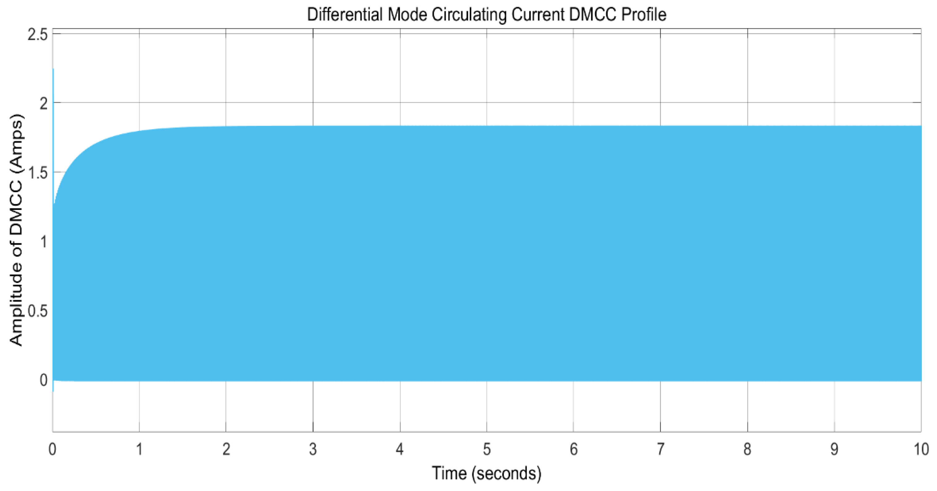
This proposed control scheme can also play a vital role in eliminating the circulating currents, i.e., DMCCs, as a parallel-connected converter scheme is under consideration. To show the robustness of the converter, a comparative case study was performed for this considered system in which the average inductor current mode controller (AICMC) was used first for observing DMCC behavior. The magnified waveform profile of these DMCCs for AICMC is shown in
Figure 18. Differential mode circulating currents for AICMC are shown in
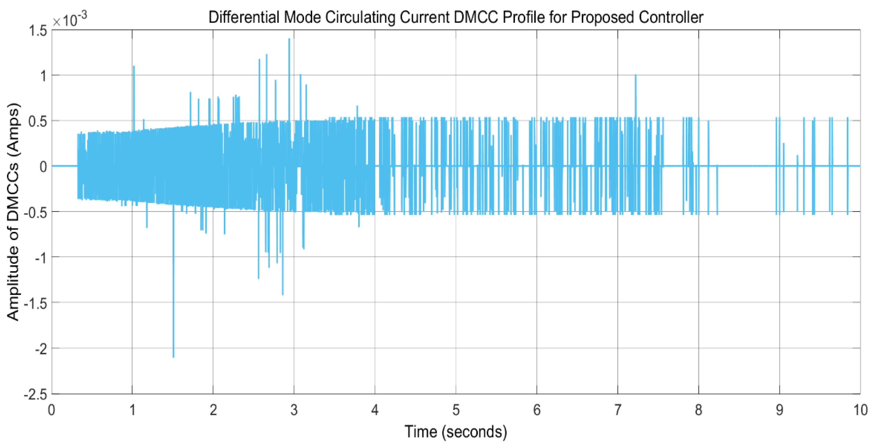
Figure 19, which means that currents still exist between two converters, and, similar to each parallel-connected converter, these can be dangerous for MOSFETS. Therefore, by applying the proposed controller to the system, the DMCCs for the first two connected buck-boost converters are shown in
Figure 20, which shows that circulating currents in terms of the parallel connection of the converters are eliminated efficiently.
For a more generic comparison performance, the case study from literature reference [
24] is considered, where the same case of parallel-connected power electronics converters is shown for circulating current control. Two different control schemes, i.e., the droop control method and the sliding-mode control method, are presented to control circulating currents and load power sharing amongst parallel-connected modules. A comparison is presented in terms of circulating current elimination, where the sliding-mode control presents better results (with circulating current value of ±0.05 A) than the droop control method (with circulating current values of ±1 and ±0.2 A). The comparison of these control scheme values with the values of our proposed control scheme (circulating current value of ±0.005 A, shown in
Figure 19) shows the performance superiority of our proposed control scheme.
In addition, the THD analysis for the comparison study performed between our proposed control scheme and the AICMC control scheme was also considered. The THD profile for AICMC control is shown in
Figure 21. In the case of AICMC, the THD for the system under consideration is 15.67% which provides a power factor of about 0.9. Thus, by comparing
Figure 21 with
Figure 15, it can be concluded that our proposed scheme is not only effective in eliminating circulating currents, but also in eliminating the harmonics distortion factor. Taking Equations (40) and (41) into account, a higher power factor is maintained in terms of using our proposed control scheme as compared to the AICMC control scheme.
9. Microcontroller Hardware Validation of Proposed Control Scheme
To validate the control algorithm, it was implemented on a TI TMS320F28379D microcontroller with a time-averaged model of the PFC. Similar to hardware-in-the-loop (HiL) testing, the PFC was emulated in real-time to provide feedback to the controller, eliminating the need for a physical prototype of the converter. In this case, the emulation was performed on the same hardware as the control algorithm, differing from HiL by the absence of dedicated hardware for emulation and a corresponding electrical interface.
Due to the limited computing power of the microcontroller compared to commercially available real-time emulators, a time-averaged model, which is executed once every switching period, was chosen. This discrete-time model consists of the equations for the inductor currents and the output capacitor voltage:
In the case of three parallel-connected converters, the equations for inductor currents will be:
As the output of all the converter finally converges to the same load, we can take the average output voltage as follows:
The whole process of validation of our control scheme along with the converter plant model is shown in
Figure 22. Both the control algorithm and the plant model were implemented on the microcontroller to be executed at 10 kHz. Noise is added to the inputs of the control block to compensate for the fact that these are not physical signals. At each sampling time, the state of the PFC is visualized via serial communication or using the on-chip digital-to-analog converters (DACs). The results obtained for this real-time digital hardware validation of our proposed system are shown in
Figure 23,
Figure 24,
Figure 25 and
Figure 26.
The output voltage profile of the scheme comprising three parallel-connected controls is maintained at 400 volts as shown in
Figure 23. The inductor current profiles in parallel-connected converters for the different values of inductors are shown in
Figure 24 and
Figure 25, respectively. The profile for the rectified input voltage along with the inductor current/line current (for same values of inductors) is shown in
Figure 26, which shows that the line current is molded finely according to the input supply voltage. The execution times of both the control algorithm and the time-averaged PFC model were measured and are presented in
Table 2.
Table 2 shows the computation time of the full emulation and of only the control algorithm at a clock frequency of 200 MHz. Only CPU1 was utilized for the validation. The CPU load of the control algorithm was calculated taking into account that the currents and voltages are sampled at the midpoint of the PWM period, while the duty cycle needs to be updated at the end of the PWM period, effectively halving the available computation time.
10. Conclusions
Digital feed-forward control for parallel-connected PFCs is proposed in this paper. Buck-boost converters, operating in CCM and DCM, are the focus in this scheme to derive the feed-forward control. Both operating modes of the converters are studied in detail in this article. The proposed control scheme is derived first for a single converter and then expanded for the converters connected in parallel. As in parallel connection of power converters, the problem of circulating currents occurs, which is also discussed. All the types of circulating current and their elimination methods are also included in this control method, which makes it more efficient and valuable. Methods of improvements for this control scheme are also suggested in the form of an optimization process to improve the power factor by bringing it closer to unity. Simulation was undertaken to perform load sharing and the voltage regulations implemented by the proposed feed-forward control method. Duty cycles that deliver the unity power factor are generated efficiently by the proposed scheme. Harmonics in the current waveform are abolished, making it in phase with the line voltage. The power factor is also enriched to the unity. Validation was also performed in terms of using HIL validation of our scheme, where we used a C2000 MCU launchpad for our testing. For the purpose of comparison and highlighting the better operation of our control scheme, the same power system was connected across the AICMC control method to observe the results and compare them with our proposed control scheme. Then, more recent research work and control methods, i.e., sliding-mode and droop control methods, and their results, are also presented to show the effectiveness of the proposed control method. The comparison of these methods and their results shows that our proposed control scheme has more potential in terms of voltage and current regulation, and in the control of circulating currents.


