Review

Recent Advances in the 3D Printing of Pure Copper Functional Structures for Thermal Management Devices

by
Yue Hao Choong
1,2,
Manickavasagam Krishnan
1 and
Manoj Gupta
2,*
1
Advanced Remanufacturing & Technology Centre (ARTC), Agency for Science, Technology and Research (A*STAR), 3 CleanTech Loop, #01-01 CleanTech Two, Singapore 637143, Singapore
2
Department of Mechanical Engineering, College of Design and Engineering, National University of Singapore, 9 Engineering Drive 1, Block EA, #07-08, Singapore 117575, Singapore
*
Author to whom correspondence should be addressed.
Technologies 2023, 11(5), 141; https://doi.org/10.3390/technologies11050141
Submission received: 13 September 2023 / Revised: 11 October 2023 / Accepted: 13 October 2023 / Published: 15 October 2023
(This article belongs to the Collection Review Papers Collection for Advanced Technologies)

Abstract

:
Thermal management devices such as heat exchangers and heat pipes are integral to safe and efficient performance in multiple engineering applications, including lithium-ion batteries, electric vehicles, electronics, and renewable energy. However, the functional designs of these devices have until now been created around conventional manufacturing constraints, and thermal performance has plateaued as a result. While 3D printing offers the design freedom to address these limitations, there has been a notable lack in high thermal conductivity materials beyond aluminium alloys. Recently, the 3D printing of pure copper to sufficiently high densities has finally taken off, due to the emergence of commercial-grade printers which are now equipped with 1 kW high-power lasers or short-wavelength lasers. Although the capabilities of these new systems appear ideal for processing pure copper as a bulk material, the performance of advanced thermal management devices are strongly dependent on topology-optimised filigree structures, which can require a very different processing window. Hence, this article presents a broad overview of the state-of-the-art in various additive manufacturing technologies used to fabricate pure copper functional filigree geometries comprising thin walls, lattice structures, and porous foams, and identifies opportunities for future developments in the 3D printing of pure copper for advanced thermal management devices.

1. Introduction

3D printing, also known as additive manufacturing (AM), has gained traction as an industrial manufacturing solution for complex geometry components. This is due to its inherent advantages in the freedom of design and integration of functional parts that result from a layer-by-layer fabrication process. For thermal management devices such as heat sinks and heat exchangers, which consist of multiple fins or internal passageways that are constructed out of thin wall geometries and lattice structures, AM is an appealing alternative to conventional manufacturing processes such as subtractive machining. This is illustrated in Figure 1, which visually highlights the differences in channel geometries for a cold plate heat sink that are possible with AM compared to traditional machining. The AM channels, formed as topology-optimised lattice structures, can increase the amount of surface area that is available for heat transfer within the smallest volume possible, while still facilitating smooth fluid flow with minimal pressure losses in contrast to simpler linear geometries [1].
Until recently, the development of metal AM hardware and processing technologies has generally focused on improving the performance of structural metals such as steels, nickel alloys, titanium alloys, and aluminium alloys. High levels of dimensional accuracy and geometrical complexity, as well as material properties that are comparable to mature refinement techniques, can now be routinely obtained from various commercial AM solution providers [3,4,5,6,7]. However, while these materials could be 3D printed into the form factor of a heat sink or heat exchanger, with the exception of aluminium alloys, many are not expected to see typical use in advanced thermal management devices due to their lower thermal conductivities, as shown in Table 1. For example, in the comparison of two identical-geometry heat sinks, manufactured using 316L stainless steel and aluminium 6061, respectively, using selective laser melting AM, Wong et al. [8] noted that the aluminium heat sink was able to transfer more than twice the heat of the stainless steel heat sink for Reynolds number > 2000.
Nevertheless, continuous efforts have been made to increase the performance limits of additively manufactured thermal management devices with less-than-ideal material properties, and enhancements to heat transfer capabilities ranging from 10% to 40% have been achieved over their conventionally manufactured baseline counterparts [10]. Eventually, however, a combination of both optimal material properties and design geometries will be necessary to achieve a true performance breakthrough in additively manufactured thermal management devices towards next-generation levels.
In this context, AM technology has progressively matured over the past five years. The recent emergence of industrial-grade 3D printers in the commercial market that are now equipped with higher power 1 kW lasers (100–400 W typical) in the near-infrared (NIR) spectrum (1060 nm) [11], as well as short-wavelength green lasers (515 nm) [12,13] has created new opportunities for manufacturers of thermal management devices to 3D print pure copper beyond the laboratory level. Pure copper, the quintessential material known for its outstanding thermal and electrical conductivities that are approximately double that of aluminium, could previously not be processed via Laser-Powder Bed Fusion (L-PBF), the most widely used metal AM process, to sufficiently high density and conductivities. This is due to the inherently high optical reflectivity of copper to NIR irradiation [14], which is the typical wavelength of laser units used in commercial L-PBF printers. As a result, the complete melting and fusion of the copper feedstock particles cannot occur. In severe cases, stray back-reflections of the laser can result in damages to the optical system of the 3D printer (see Figure 2) [15]. Hence, the lack of printability for copper has hitherto been a major obstacle in the additive fabrication of thermal management devices [16].
Although the literature on the AM processing of high-purity copper has been recently reviewed by Romano et al. [17], Jiang et al. [18], Campagnoli et al. [19], and Tran et al. [20] between 2019 and 2022, a gap is noted in the concise evaluation of state-of-the-art 3D printing of pure copper functional geometries with fine or filigree features that are specific to thermal management devices. To the best of the authors’ knowledge, the only review on the AM of copper for thermal management applications was previously published in 2017 by Singer et al. [16], before the wider availability of commercial L-PBF printers that are equipped with high-power or short-wavelength lasers. Hence, this literature review article aims to provide an analysis of recent developments in the AM processing of copper, with a focus on thin walls, lattice structures, and porous foams using various AM technologies. The authors hope that this article can aid the larger scientific community and manufacturing industries in identifying further opportunities to utilise the advantages of AM for thermal management applications for an increasingly digitalised and energy-conscious society.
In the following sections, the working principles of common thermal management devices and opportunities for performance enhancements are first introduced. Next, an overview of the different AM techniques is presented and the benefits of AM at addressing conventional manufacturing challenges are briefly discussed. Following this, an analysis of market-ready AM processes to 3D print pure copper is conducted, which represents the baseline capabilities of copper AM technology that manufacturers of thermal management devices can pragmatically implement today. Subsequently, findings from recently published scientific studies are assessed to determine the state-of-the-art developments in the field, with a focus on the processibility of filigree geometries and their corresponding material properties for use in advancing thermal management devices. Lastly, an outlook is presented on where future research and developmental efforts for AM of pure copper can be made to better address both the current and future needs of thermal management devices.

2. Thermal Management Devices

2.1. Common Examples and Operating Principles

Thermal management devices are used to maintain a system within its operating temperature range by controlling the quantity of heat inflows and outflows. Some common examples include heat sinks, heat exchangers, heat pipes, and vapour chambers, and their basic operating principles are summarised in Figure 3. Thermal management devices can be used individually, or together in various configurations as a collective thermal management system, such as in heating, ventilation, and air-conditioning (HVAC) building infrastructures. A brief description of the four common thermal management devices is as follows:
Heat sinks are finned metal devices that are frequently found on top of computer chips to provide cooling. Heat from the computer chip is first conducted into the heat sink via direct physical contact. It is then dissipated away into the ambient environment through extended fin surfaces via the natural convection of air, or via forced convection if a fan is used [21]. When water is used as the working fluid instead of air, the heat sink is known as a cold plate. Since only one type of working fluid is used in heat sinks, they are classified as single-fluid domain thermal management devices.
Heat exchangers are devices that enable heat exchange between two working fluids at different temperatures [22]. Since the fluids are fundamentally not intended to mix during operation, they must be kept separated by high thermal conductivity thin-walled structures in lattice shell or channel configurations, which are designed to be impermeable to the fluids. The main feature that distinguishes heat exchangers from heat sinks is that heat exchangers involve at least two working fluids or mediums and are thus multiple-fluid domain thermal management devices.
In their basic configuration, heat pipes are closed tube vessels that contain a working fluid and porous wick structure within an internally sealed vacuum environment. During operation, heat pipes utilise a continuous cycle of the evaporation and condensation of the encapsulated working fluid to transfer heat rapidly between the hotter side (evaporator) and colder side (condenser) [23]. As the liquid working fluid absorbs heat energy at the evaporator end, it vaporises and diffuses along the tube towards the condenser end due to an evolving pressure gradient, and thus carries along a significant amount of thermal energy in the form of the latent heat of vaporisation. This thermal energy is then spontaneously released into the cooler condenser, and the working fluid condenses back into a liquid which is returned to the evaporator through the porous wick structure via capillary forces, and the cycle repeats.
Vapor chambers operate similarly to heat pipes; however, their design allows heat to be transferred or spread in a planar manner rather than along a single axis [24].
Figure 3. Schematic and basic operating principles of a (a) heat sink [21,25], (b) heat exchanger [26,27,28], (c) heat pipe [23,29], and (d) vapour chamber [24,30].
Technologies 11 00141 g003

2.2. Common Examples and Operating Principles

Well-implemented thermal management solutions facilitate safe, reliable, efficient, and high performing systems across multiple engineering domains and applications. For example, the operating temperatures of lithium-ion batteries used in electric vehicles significantly affect their output power, charge capacity, internal resistance, charging performance, and total lifetime before failure [31,32]. In severe cases, overheated batteries can even result in fire and explosion hazards due to thermal runaway [33]. New frontiers in thermal management solutions for electric vehicle batteries are therefore being continuously pursued to keep temperatures within the optimal range of 15 °C to 35 °C [34], while simultaneously ensuring that temperature variances across individual cells do not exceed 5 °C [35], as electric vehicles place increasingly greater demands on their batteries for better range, faster charging times, and enhanced output performance.
In the domain of digitalisation and microelectronics, Moore’s law predicts that the number of transistors on an integrated circuit would approximately double every two years, which inadvertently results in an accelerated emergence of high performance computer chips and electronics packaging with high packing densities and high heat fluxes [36]. To maintain an operating temperature below 85 °C, modern computer chips require cooling capabilities of as much as 300 W/cm2 [37], which is equivalent to dissipating the amount of heat produced simultaneously by five hair-dyers for the same unit area. Thus, as microelectronics continue to evolve in an increasingly digitalised world, the cooling performance of next-generation thermal management devices will have to exponentially advance as well [37,38].
From a global sustainability perspective, the impending onset of climate change has spurred worldwide efforts towards net-zero carbon emissions by 2050, under the Paris Agreement [39] and United Nations Net-Zero Coalition [40]. Against the backdrop of increasingly strict carbon tax legislations and rising energy prices, the International Energy Agency has determined that enhancements to renewable energy technology and improvements to energy efficiencies will be critical in the near term for achieving a 50% reduction in global emissions by 2030 [41]. Here, breakthroughs in thermal management devices and systems are integral to elevating the capabilities of the infrastructure used to generate and store clean energy, such as solar panels [42,43], wind turbines [44,45], geothermal energy systems [46,47], hydrogen generation and storage [48,49,50,51], and nuclear power plants [52,53]. Moreover, in commercial air travel, which is currently the mode of transport with the fastest growth in greenhouse gas emissions [54], enhanced thermal management in gas turbine aero engines are key to reducing emission levels, increasing fuel economy and improving flight safety by preventing the build-up of carbon lacquer that can choke fuel lines [55].

2.3. Potential Ways to Improve Thermal Management Devices and the Limitations Faced

Potential ways to increase the performance of thermal management devices are as follows. In the modelling and simulation of new heat exchanger designs, triply periodic minimal surfaces (TPMS) such as Gyroid and Schwarz-D lattice structures have been found to improve heat transfer capabilities by up to 120% more than the linear channel geometries used in a printed circuit heat exchanger (PCHE) for the same pumping power, as shown in Figure 4 [56]. This is due to the increase in the specific heat transfer surface area of the lattice geometries, and greater mixing that is promoted by the increased hydraulic tortuosity of the lattice flow paths [57].
One caveat, however, is that surface area and tortuosity cannot be pragmatically increased indefinitely by using smaller and more numerous lattice cells to improve heat transfer performance. This decreases permeability, and according to Darcy’s law [58] that governs the fluid flow of dynamic viscosity μ through a homogeneous porous medium of uniform cross-sectional area A ; flow rate Q is directly proportional to the product of permeability k and the pressure drop across the porous medium Δ P over length L , as shown in Equation (1).
Q = k A μ L Δ P
Hence, any loss in permeability needs to be negated by using a higher pumping power to maintain the same flow rate, which comes at the expense of a larger pump or the increased wear and tear of the pump. At the same time, the physical construction and inspection of smaller cellular units would also be more challenging, which ultimately increases manufacturing costs.
Care should therefore be taken in designing and selecting the appropriate lattice structure and unit cell size to maximise heat transfer performance while keeping pumping power and manufacturing costs minimal. While the optimal design will vary depending on functional requirements, some reference guidelines can be taken from Table 2, which provides a short summary of various TPMS designs from the available literature that are benchmarked against a conventional reference.
In the case of natural convection heat sinks, large scale computational modelling with an order of 20 to 330 million state degrees of freedom was used to identify the most effective heat dissipation geometries. Through a multi-physics Navier–Stokes and Bousinessq approximation framework, the solutions spontaneously converged into organic branch-like fractal geometries over a wide range of Grashof numbers between 103 and 106, as shown in Figure 5a. This continues to hold true even after 1000 iterations, as shown in Figure 5b [62].
Meanwhile, in heat pipes and vapour chambers which utilise internal wicks to circulate a working fluid via vapour diffusion and capillary flow to transfer heat, integrated hierarchical micro-porous structures with grooved geometries (see Figure 6) can enable an optimal balance of high capillary pressure to drive fluid flow over longer distances and against the effects of gravity while still retaining high vapour permeability [63,64].
Despite the promising potential of these solutions, physical fabrication of the filigree geometries will remain a challenging feat as long as manufacturers continue to rely on conventional processes such as casting, sintering, forming, and subtractive machining in the production of thermal management devices [65,66,67]. Although established, these processes inadvertently approach a technological limit in terms of the possible complex features. For example, three-dimensional lattice structures cannot be fabricated using subtractive machining due to lack of direct access for physical tooling, while porous structures are at risk of crushing, blockages, and torn cellular ligaments when being machined into the required geometry for assembly, as shown in Figure 7. Even with the use of wire electric-discharge machining, partial melting of the machined surface resulted in pore fusion and closure of the recast layer. This had to be removed in turn by a secondary acid etching process to expose the underlying open-cell pores, which in itself is also a challenging process, before good surface uniformity can be achieved [68].

3. Additive Manufacturing

3.1. Overview

Additive Manufacturing (AM) is a direct digital-to-physical manufacturing technology that deposits feedstock material, one layer at a time, according to the two-dimensional cross section of the digital part model.
From an overarching manufacturing supply chain and logistics perspective, the direct digital-to-physical nature of AM facilitates decentralised manufacturing—a digital file can be uploaded into the computing cloud and printed from anywhere in the world without the need for extensive tooling and fixtures. As an example of how AM can increase supply chain resilience, one would need to look no further than the recent COVID-19 pandemic to witness its rapid response in alleviating local shortages of healthcare consumables and facilities, improving the comfort levels of personal protective equipment, and in situ fabrication of visualisation and training aids to help cope with the limited number of trained healthcare workers [69]. Hence, for manufacturers in the large-scale distribution of thermal management devices and systems, decentralised manufacturing through AM can provide a competitive edge in both cost and lead times. Moreover, as a secondary benefit of direct digital-to-physical fabrication, manufacturers can also readily customise their product offerings according to the geographical location of the additive manufacturing facility on site. For example, the battery thermal management systems of electric vehicles in temperate and tropical regions will differ according to the range of environmental temperatures that the vehicle will be exposed to during operation. Hence, designs of thermal management devices should cater for stronger heating performance in vehicles that will experience colder climates due to range reduction at low temperatures (see Figure 8).
At the product level, the bottom-up approach in the selective deposition of feedstock material intrinsically enables AM to fabricate the required functional geometries without being subjected to conventional manufacturing constraints [71]. As previously mentioned, filigree geometries and internal channels that would have otherwise been highly challenging or even impossible to fabricate using forming and subtractive machining, due to reasons such as lack of direct tooling access or structural strength to withstand cutting forces, are all feasible to be produced using AM [72]. Without such manufacturing limitations, benefits are abundant, such as light-weighting, an increased strength-to-weight ratio, reduced raw material wastages, higher assembly reliability through parts consolidation, and increased cost-effectiveness due to a lower parts count [73]. One such example is a hydraulic actuator valve block, shown in Figure 9, that is used to control flight surfaces of the Airbus A380. The flight-certified titanium alloy AM valve block, while fulfilling identical functionalities to the conventionally manufactured counterpart, was also 35% lighter and reduced the total parts count by 10 [74].
Essentially, the versatile and agile nature of AM offers numerous advantages from a production perspective in terms of mass customisation, shortening the supply chain, on-demand production of spare parts, and overall improved cost-effectiveness and lead times [75].
Today, many similar AM processes exist under different commercial trademarks. To help better identify them, these AM processes can be grouped into seven families of technologies based on their shaping methodologies in accordance to ISO/ASTM 52900 [76]. A summary of the working principles, unique strengths, and typical materials processed for each of these AM technologies is provided in Figure 10 [77].

3.2. Market-Ready AM Solutions to 3D Print Pure Copper

As one of the most thermally conductive materials known to humankind that is still cost-sensible (the other alternatives being diamond, gold, and silver), copper has traditionally been the preferred choice of material for manufacturing thermal management devices.
Assuming full density (8.96 g/cm3 at room temperature), the high thermal conductivity of copper at close to 400 W/m K will then be predominantly determined by its purity levels (see Figure 11), since contaminants can act as electron and phonon scattering sites within the metal lattice and disrupt the ability to transfer heat by reducing mobility [78,79]. Hence, conventional copper refinement processes have been gradually developed over the past 150 years to yield at least 6N levels of purity (99.9999% pure copper) today [80,81].
Recently, the 3D printing of pure copper (>99.8% pure) has begun to emerge as the market-ready commercial solutions from several key AM manufacturers and providers (see Table 3). This is a game-changer for AM designers of thermal management devices, since aluminium alloys had previously been the only practical option for applications requiring high thermal conductivity (the thermal conductivity of aluminium is approximately only half that of pure copper).
While the properties of these commercial copper printing solutions seem to be already sufficiently well-established to create the advanced geometries shown in Figure 12, it is likely that further investigations will be required to determine the feasibility of meeting the actual functional requirements of thermal management devices.
For example, many commercial AM providers at present (see Table 3) do not clearly define the properties of their copper printing solutions for thin-wall structures, which are incidentally the main functional features of heat sinks and heat exchangers. From this perspective, it is notable that multiple studies have reported stark differences in dimensional accuracy, geometrical distortion, surface roughness, density, microstructure, mechanical properties, and overall printability between bulk regions and thin-wall structures for different materials and AM processes [90,91,92,93,94,95]. It is thus likely that completely new and different process parameters and print strategies from what have already been established in existing commercial solutions will be required before dense and well-formed thin-wall copper structures with high thermal conductivity can be obtained. This is particularly critical for liquid-based heat sinks and heat exchangers to prevent leakages and cross-contamination of the working fluids. Therefore, in the next section, the state-of-the-art is critically assessed to determine the true capabilities in the AM of pure copper filigree geometries.

4. State-of-the-Art in the AM of Pure Copper Filigree Geometries

4.1. Thin-Wall Structures

Recently, in 2019, Guan et al. investigated the L-PBF fabrication of pure copper thin-wall grid-like structures (see Figure 13a) using a typical 1060 nm NIR wavelength laser with a beam spot size of 80 µm [96]. At a laser power of 190 W and scan speed of 500 mm/s, thin walls of 0.2 mm, 0.3 mm, and 0.5 mm thickness were formed. Despite the use of a meander exposure strategy with a hatching distance of 60 µm (see Figure 13b) that imparted additional energy from multiple meltpool overlaps compared to single laser scan tracks, the authors observed that the thin walls consisted primarily of discontinuous meltpool beads that were only partially fused together (see Figure 13c,d). Furthermore, some powder particles could also be found trapped in the cave-like pores formed between adjacent semi-fused beads, especially at the intersections of the grid-like structure (see Figure 13e). To achieve further densification, the authors proposed the use of higher power 500 W lasers in combination with several laser remelting exposure strategies. At the same time, it is also advisable that the energy input should not be overly excessive. This would increase the susceptibility of filigree geometries to the denudation effect [97], whereby the depletion of metal particles occurs in the immediate vicinity of the solidified track and is caused by the outwards meltpool vapor pressure created during laser exposure. When multiple thin walls are closely packed together such as in the case of a mesh structure, the formation of a large denudation zone can result in an uneven powder bed for the next deposited layer.
In the same year, Silbernagel et al. [99] conducted a L-PBF process parameter study on free-standing pure copper thin walls 18 mm in length and 4 mm in height (see Figure 14a). The 3D printer used was equipped with a laser unit of 1070 nm wavelength and beam spot size of 35 µm. The authors investigated three different laser powers of 100 W, 150 W, and 200 W, three different layer thicknesses of 30 µm, 45 µm, and 60 µm, and a scan speed ranging from 150 mm/s to 1250 mm/s in increments of 25 mm/s. Also, instead of the meander exposure strategy used by Guan et al. [96] in the previous study, the authors utilised a single-line laser scan track that was repetitively stacked at every layer to form the planar wall. Hence, the wall thickness would be solely dependent on the size of the meltpool in the powder bed. Regarding layer thickness, the authors observed that the use of 45 µm layers resulted in a good balance of powder spreadability and melting behaviour, therefore it was used for the rest of the study. The 30 µm layers resulted in powder spreading issues, which ultimately resulted in missing sections in the thin walls. Conversely, 60 µm layers resulted in inconsistent meltpool tracks, which exhibited sintering rather than melting characteristics and further indicated that the energy was insufficient for full-depth penetration into the thicker deposited layer. For laser power, the authors found that improvements to the continuity of the thin walls were insensitive to different combinations of laser powers or different orders of those powers, even when multiple scans over the same track were made. In fact, repeated passes at high laser powers resulted only in a detrimental balling effect on the thin walls. Here, the effects of denudation for thin-wall structures when using remelting strategies at high laser powers are re-emphasised. For the scan speeds, the authors found that while the highest, 1250 mm/s, scan speed could provide sufficient energy to form a thin wall, bonding was minimal, which resulted in very thin walls of low strength. Subsequently, by comparing the continuity of the meltpool tracks and wall thickness, the authors were able to identify an optimal scan speed of 300 mm/s.
Additionally, Silbernagel et al. [99] also investigated the changes in the chemical composition of the pure copper meltpool when a steel substrate is used. Due to the low thermal conductivity of steel, it has now become a common approach to use steel substrates instead of copper substrates to prevent rapid heat loss from the meltpool during the L-PBF of pure copper, especially during the critical initial layers to prevent delamination. Here, the authors found through EDX analysis that a considerable amount of iron had diffused into the meltpool for the first 1.5 mm in the vertical build direction, which resulted in a physical bulging of the thin walls (see Figure 14b,c). Nonetheless, at higher build heights, the copper concentration returned to near 100% purity levels and any previously iron-contaminated layers did not remelt, which prevented further diffusion of iron along the build direction. Physically, this is marked by a notable decrease in wall thickness past the iron-contaminated zone.
To overcome the key challenge of meltpool heat loss encountered by long-pulse or continuous wavelength lasers that are common to many L-PBF printers, Kaden et al. first explored the use of ultrashort pulse (USP) femtosecond lasers in 2017 [100]. The authors theorised that the extremely short interaction times between the USP laser and the powder feedstock would drastically minimise heat loss from the meltpool during laser exposure, and thus be able to retain a greater amount of energy for the complete melting and fusion to occur. Furthermore, the confinement of the active heating zone to the immediate vicinity of the illuminated area would also enhance the precision and resolution of filigree copper geometries. As a result, the authors were able to fabricate homogenous thin-wall structures of approximately 100 µm in wall thickness with a height-to-width aspect ratio of 15:1 (see Figure 15a). However, incomplete fusion was still clearly observable through scanning electron microscopy (see Figure 15b). The authors attributed the lack of densification to a non-optimal ratio of beam spot size to particle diameter, by reasoning that since only particles that underwent direct laser exposure would melt and fuse together to form a bead, using particles and beam spot diameter of the same size order (35 µm) would prevent the consolidation and fusion of adjacent particles into the meltpool during exposure.
In a later study [101], Kaden et al. compared the performances of USP lasers at 1030 nm (NIR) and 515 nm (green) wavelengths in fabricating thin-wall structures (see Figure 15c,d). While the beam spot size of both lasers was similar, hardware restrictions limited the power output of the green laser to half that of the NIR laser. In comparison to the NIR laser, a smaller layer thickness of 15 µm instead of 30 µm was used for the green laser, as well as a smaller particle size of 10 µm instead of 25 µm. The authors observed that the thin walls produced by both lasers yielded highly similar geometrical resolutions and morphologies, with an average wall thickness below 100 µm (see Figure 15e,f). This suggested that the effective energy absorbed by the illuminated copper feedstock at 515 nm is approximately double that of 1030 nm. Regardless of laser wavelength, however, full densification could still not be achieved. Nonetheless, the power output produced by the USP lasers at 11 W (green) and 24 W (NIR) needs to be taken into consideration, which is extremely low compared to the 1 kW laser systems available today. Moreover, the ability of the copper feedstock powder to even melt and fuse together at such low levels of output in the first place is evidence of the latent potential of USP lasers. For example, in further investigations with the green USP laser for actual engineering components, Kaden et al. [102] were able to achieve filigree copper geometries such as complex organic structures (Figure 15g), reduce the strain and support structures for thin overhanging regions (Figure 15h), and produce thin-wall structures with extremely high aspect ratios of 70:1 (Figure 15i).
In another attempt to improve densification of thin-wall structures, Ma et al. [103] investigated the influence of using higher NIR laser powers of up to 500 W for various scan speeds and hatching distances on the relative density, surface roughness, and wall thickness of thin-wall copper flanged samples (see Figure 16a,b).
At higher laser powers above 400 W, the authors were able to consistently obtain relative densities of the thin walls above 99%, as shown in Figure 16a. In fact, unlike the insensitivity of the meltpool to changes in laser outputs below 200 W [99], the authors found that when the laser output was increased from 200 W to 300 W, the relative density could be significantly improved to nearly full density levels, regardless of the scan speeds or hatching distance used (see Figure 16c). Hence, it seems that a minimum output of 300 W would be required for NIR lasers before full densification could be obtained. However, there is a trade-off in dimensional accuracy when higher laser powers are used, with physical wall thickness ranging from two to four times that of the digital model. While the authors could compensate for the additional material by simply reducing wall thickness in the digital model to 50 µm to achieve the desired value of 200 µm for the physical part, it is noted that such an approach could be challenging to implement for complex finned structures of varying cross-sectional areas such as in topology-optimised heat sink geometries. The authors also found that the exposure strategy played an important role in determining the wall thickness and surface roughness of the parts. In general, implementing a circular scanning strategy that conformed to the cylindrical geometry of the parts instead of a generic linear scanning strategy (see Figure 16d) produced more accurate wall thicknesses and lower surface roughness (see Figure 16e). Here, further developments in customised geometry-dependent exposure strategies for filigree geometries beyond basic primitive shapes are highly anticipated due to the potential scale of improvements that can be unlocked with this technique.
So far, the fabrication of pure copper thin-wall geometries via typical NIR lasers with an output below 200 W does not seem capable for obtaining fully dense or near fully dense structures. This is further affirmed through the work of Jadhav et al. [104], who used an empirically validated analytical model for the L-PBF processing characteristics of pure copper at laser powers ranging from 200 W to 500 W with different scan speeds (see Figure 17a).
While no thin-wall structures were investigated, the authors were able to obtain relative densities exceeding 99% for bulk pure copper specimens using a 1080 nm wavelength laser with beam spot size of 37.5 µm, laser power of 500 W, and range of scan speeds corresponding to a volumetric energy density window of 230 to 310 J/mm3. A standard L-PBF powder feedstock size of 25–60 µm was used.
Perhaps of greater interest is that the analytical model categorised the L-PBF processing of pure copper into two different processing windows—the conduction regime and keyhole regime (inclusive of keyhole-induced porosity, see Figure 17b). The authors found that for highly reflective materials such as copper to be fully densified using NIR lasers, the processing window needs to occur in the keyhole regime. The formation of keyholes is the critical factor that enables full densification to occur, since effective laser absorption is exponentially increased by the presence of multiple internal reflections of the laser within the keyhole, as shown in Figure 17b. However, the keyhole also needs to be stabilised through an optimal processing window—in essence, for copper, since the bottom half of the keyhole absorbs approximately four times the amount of laser energy as the top half of the keyhole [105], it is more likely to remain in the molten state while the top half solidifies earlier [106]. This will result in trapped or keyhole-induced porosity within the material, which is exacerbated by introducing overly large amounts of volumetric energy density. Conversely, too little volumetric energy density places the L-PBF of copper into the conduction regime, in which most of the laser energy is reflected or dissipated away instead of being absorbed by the meltpool. Hence, for typical copper feedstock sizes at NIR wavelengths, this corresponds to the narrow processing window of 230 to 310 J/mm3 (see Figure 17c).
However, the authors also concluded that it is the formation of stable keyhole features, rather than the laser power per se, that enables the production of bulk solid copper at full densities. Hence, it follows that as long as optimal keyholes can be formed, it will still be possible to obtain the full densification at laser powers below 500 W by optimising other key process variables in L-PBF such as particle size, baseplate material, and platform heating, modifying the surface of the copper feedstock for higher optical absorption of NIR (1060 nm) wavelength laser energy, or using green (515 nm) or blue (450 nm) wavelength lasers which have inherently better absorptivity by non-modified copper powder particles (see Figure 18).
Such approaches were indeed used by Qu et al. [108], who were able to obtain pure copper bulk components with a relative density of 99.6% at 200 W of NIR laser output from a high precision L-PBF system with a small beam spot size of 25 µm, fine power particles between 5 µm and 25 µm, a small layer thickness of 10 µm, and 316 L stainless steel substrate. The authors were also able to achieve an electrical conductivity of 96% IACS after the heat treatment of the components, which suggests an ideal thermal conductivity that is near to the theoretical limits of copper. Thin-wall structures using an exposure strategy of single-line scan tracks (see Figure 19a,b) were also fabricated over a range of laser powers and scan speeds (see Figure 19c).
The authors observed processing characteristics similar to what had been reported by Jadhav et al. [104]—lack of fusion, densification, and overfusion (see Figure 19c,d), Nonetheless, the inherently high precision of the printer and material feedstock system lend themselves well to producing high-density thin walls with low surface roughness between Ra 3 and 5 µm (see Figure 19e), and wall thicknesses as low as 150 µm. The meltpool depth was also found to be well-controlled and ranging between 50 and 100 µm depending on the process parameters used (see Figure 19f), which is important in three-dimensional shell-based triply periodic minimal surface lattice structures consisting of vertical thin walls, as well as horizontal thin ‘floors’ and ‘ceilings’. Overall, the geometrical quality, surface roughness, and material properties of the filigree components fabricated by Qu et al. are highly favourable for advanced thermal management devices.
Recently, continuous short-wavelength lasers of 515 nm (green) and 450 nm (blue) have begun to emerge for use in L-PBF systems, due to the aforementioned higher energy pure copper absorptivity of these wavelengths. Contrary to NIR lasers, the current optical hardware capabilities of these short-wavelength lasers appear to have a minimum beam spot size of 200 µm [109,110,111,112,113,114], which results in an illuminated area that is up to six times as large as that of a typical 80 µm beam spot size for NIR lasers. In fact, even for the same beam spot size and laser process parameters over a range of different scan speeds, Hori et al. [110] observed that the copper meltpool bead size for a blue laser was consistently two to four times larger than that of a NIR laser (see Figure 20).
Horn et al. [112] fabricated thin-wall structures at different inclination angles of 90° (vertical), 60°, and 30° (see Figure 21a) using a continuous wavelength green laser with a beam spot size of 200 µm and maximum power of 500 W. The authors observed that while highly dense core regions of the thin walls could be achieved, an enveloping porous and branch-like structure of solidified melt beads known as ‘drips’ was also concurrently formed (see Figure 21b), regardless of laser power, scan speed, or exposure strategy used. While the extent of the drips could be reduced at more horizontal inclination angles, they could not be fully removed, and inadvertently resulted in higher surface roughness that is accompanied by an increase in wall thickness of 22% to 83% of the dense core region (see Figure 21c).
Horn et al. further noted that the presence of drips were also observed in another study on the L-PBF of pure copper using a green laser [109], however, since they only occurred around the borders of the bulk material due to the remelting of the core regions via overlapping meltpool hatching, fully dense and defect-free parts could still be obtained and the effects of the drips on bulk geometries (see Figure 21e) were considered less significant compared to filigree geometries. In the context of thin-wall structures for thermal management devices, however, the reviewed literature suggests that the current hardware capabilities of short-wavelength lasers are still not as refined as medium power (≥400 W) NIR lasers at producing high-resolution geometries with smooth surfaces for rapid heat transfer and minimal flow losses (see Figure 22).
As the scientific community continues to make progress in beam-based AM techniques to process pure copper filigree geometries, another promising group of techniques that has begun to emerge is sinter-based AM. Sinter-based AM refers to any AM process that involves a two-stage shape and sinter approach in the fabrication of 3D components. With reference to Figure 23a, the first stage involves the shaping of parts into the desired geometry either via the extrusion of a metal–polymer paste or filament through a nozzle (material extrusion), via the selective jetting of a polymer binder into the power bed (binder jetting), or via the selective curing of a metal–polymer slurry using light (vat photopolymerisation). At this stage, regardless of how the parts have been shaped, they would all consist of metal particles that are only temporarily bonded together by the polymer adhesives. In the second stage, the parts are sintered in a furnace to remove the polymer binders and form metallurgical bonds between the particles for further densification. Thus, sinter-based AM inherently avoids the poor absorptivity of copper particles to laser irradiation by removing the need for a laser to melt and fuse the particles together in the first place. Optimal selection of polymer binders and process parameters for debinding and sintering, however, will be critical to obtaining dense, dimensionally accurate, and residue-free copper parts.
For example, Yan et al. [115] utilised a paste material extrusion method to form a vase-like thin-wall cylinder (see Figure 23a) in 2018. The paste consisted of 1 µm copper powder particles (purity > 99.5%) mixed with paraffin wax at a powder to wax mass ratio of 10:1. After sintering, the authors were able to obtain thin-wall structures with a relative density of 90.4%, hardness of 80 HV, and a wall thickness of 340 µm that appears visually smooth (see Figure 23b). SEM analysis indicated high metallurgical bonding, while EDX analysis revealed that no residual carbon from binder pyrolysis was retained in the material (see Figure 23c). However, the oxygen content was around 5% by mass, which can be detrimental to the conductivity of pure copper. It is likely that the oxygen pick-up could have originated from the paste preparation in an exposed environment at elevated temperatures of 70–80 °C, during which slight oxidation of the copper particles can occur due to their high surface area to volume ratio. Further validation is required in this area. Regardless, the proper handling of specimens in sinter-based AM is required due to the lack of an inert process chamber that is inherent to beam-based powder bed fusion processes.
One of the most exciting and modern developments in the sinter-based AM of pure copper is the digital light processing (vat photopolymerisation) of a metal–polymer slurry, in which the extremely high resolution of digital light processing (see Figure 24a) in combination with a mature sintering process rooted in conventional metal injection moulding results in thin-wall structures of high density (95% bulk density), electrical conductivity (92% IACS), and thermal conductivity (92% copper standard) at just 100 µm thick [89] (see Figure 24b). This technique is currently exclusive to one commercial manufacturer, however, and future developments in this space by other AM manufacturers is anticipated.

4.2. Lattice Structures
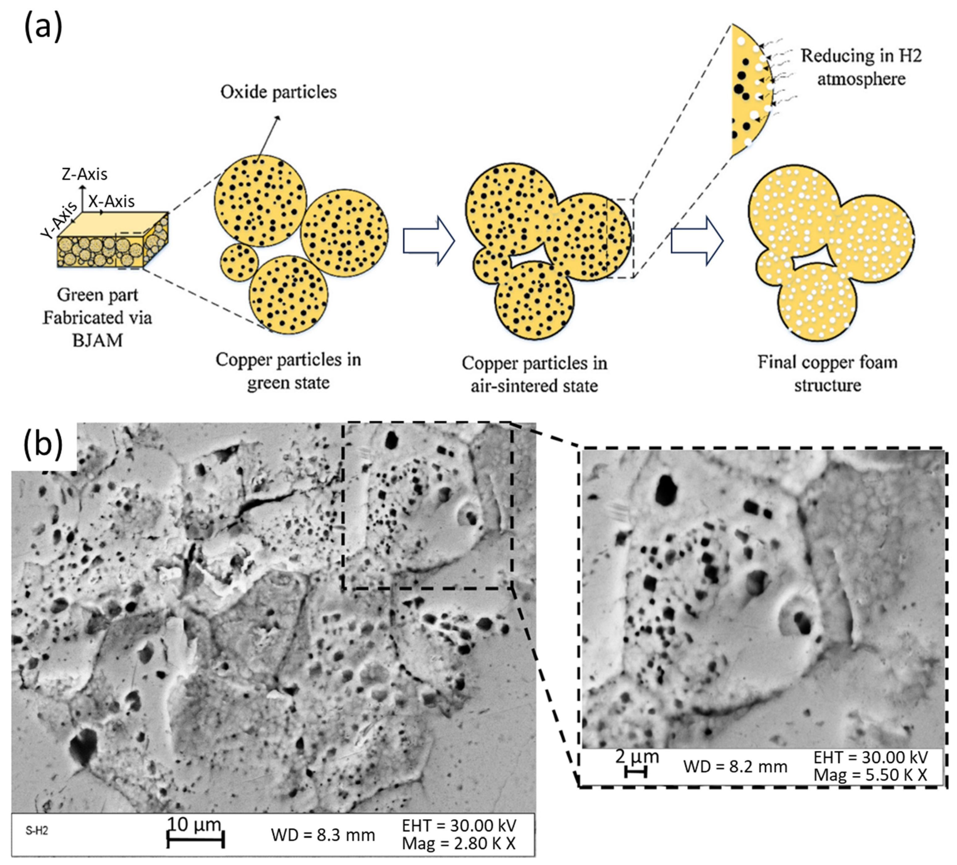
While the thin walls reviewed so far are predominantly vertically orientated features that are targeted for use as fins of single-fluid domain heat sinks, the intertwining passageways in heat exchangers with two or more fluid domains necessitate a more elaborate 3D volumetric structure in the form of TPMS shell-based lattice structures. As seen earlier in Figure 4, TPMS structures such as Gyroid and Schwarz-D are able to elevate heat exchanger performance due to an optimal balance of increased heat transfer surface area with minimal pressure losses.
By definition, TPMS are minimal surfaces that recur periodically in three independent directions, e.g., the X, Y, and Z cartesian axes [116]. Hence, TPMS lattices can be visualised as repeating unit shells that are formed by thin walls, thin ‘floors’, and thin ‘ceilings’ with smooth curvatures. This makes TPMS a more challenging geometry to produce than solely vertical thin walls for beam-based AM due to the addition of overhangs and curved surfaces that are susceptible to over-heating from excessive meltpool depth penetration (Figure 25a) and the staircase effect (Figure 25b). Nevertheless, the principles behind the AM fabrication of thin-wall structures are still applicable for TPMS lattices.
For example, Qu et al. [108] fabricated N14 and primitive-type TPMS lattice structures using their self-developed high-precision NIR L-PBF system (see Figure 26a). Optical microscopy analysis of the top surface cross-sectional area indicated a wall thickness of 100 µm with a dense and pore-free microstructure (see Figure 26b). Conversely, the side surface cross-sectional area exhibited a significantly higher wall thickness of 149 µm (see Figure 26c) due to the staircase effect. Surface roughness (see Figure 26d) was also highly dependent on build orientation and increased in order of top-facing (Ra 3.3 µm), side-facing (Ra 14.8 µm), and bottom-facing overhanging surfaces (Ra 19.2 µm). This is because at increasingly horizontal overhangs, the meltpool depth can penetrate through the overhanging region, which results in the remelting of the solidified layers and partial fusion of powder particles to the underlying surface (see Figure 26e).
In contrast to NIR lasers, lattice structures fabricated using blue and green lasers face challenges with minimum feature size and smooth surfaces [119,120], which is a similar outcome from the thin-wall geometries shown earlier. Visual examples of lattices that were fabricated using blue and green short-wavelength lasers are shown in Figure 27.
Nevertheless, NIR lasers are not without their challenges. As mentioned earlier, Jadhav et al. [104] reported that the optimal processing window for dense and well-formed pure copper structures using NIR lasers can occur only in a small range within the keyhole regime. This is further validated by Alphonso et al. [121], who conducted a comparison study of both green and NIR lasers using a benchmark artifact. Through numerical modelling and experimental verification, the authors determined that while both conduction and keyhole regimes are feasible processing windows for green lasers, only the keyhole melting regime is practical for NIR lasers. Hence, without fine tuning the process parameters for specific geometries, the use of NIR lasers in lattice structures can also result in unstable meltpools and distorted geometries [121] (see Figure 28).
In terms of the sinter-based AM of pure copper lattice structures, the technique that appears to have made the most demonstratable progress is vat photopolymerisation. Just like for thin-wall structures, the resolution, surface roughness, and surface homogeneity for TPMS lattice structures appear outstanding with this technique (see Figure 29). An improvement in isotropic properties compared to beam-based AM is also expected, due to increased grain texture homogeneity from the sintering process instead of an elongated grain structure that is characteristic of beam-based AM techniques [120]. This is critical to the thermal and electrical conductivity of pure copper since grain boundaries, especially low-angle grain boundaries with misorientation angles between 14° and 18°, induce dislocation and strain in the crystal lattice, which inhibit electron mobility and increase resistance [122]. Furthermore, the nodes of the lattice structures fabricated using beam-based AM typically contain high residual stresses due to repeated melting and solidification cycles [120].
On the other hand, the maximum relative density achievable via sinter-based AM for pure copper (<98%) is typically lower than that of beam-based AM (>99%) to date, as shown earlier in Table 3. This is due to the inherent use of polymer binders, which can leave behind residual carbon contaminants even after extensive debinding and pyrolysis processes. The necking and subsequent fusion of adjacent powder particles are thus inhibited during sintering, which results in high porosity levels [89,123]. Therefore, developments in sinter-based AM techniques for pure copper have, until now, mostly focused on improvements to densification and purity levels at the material level [123,124,125,126,127,128,129,130,131]. These efforts appeared to have paid off, as high thermal and electrical conductivities that are just shy of beam-based AM and conventionally processed copper has already been achieved for sinter-based AM techniques (see Table 3). Therefore, future work in this field is anticipated to transition towards the high-resolution printing of filigree geometries for pure copper, which is a similar journey to that previously undergone by beam-based AM.

4.3. Copper Foams

The literature that has been reviewed up to this point indicates good progress in the AM of pure copper towards addressing the manufacturing challenges of heat sinks and heat exchangers that were elaborated earlier in Section 2.3. Specifically, solutions already exist, at least at the laboratory level, to enable the AM fabrication of highly dense thin-wall geometries and TPMS lattice shells to channel fluid flow without leakages or absorption of the working fluid into the actual material.
Conversely, for heat pipes and vapour chambers, porous copper foams that function as wick structures are required whereby fluid flow is induced by capillary forces through an interconnected network of open pores which typically range from the micron to sub-millimetre in size [132,133]. Notably, unlike the voids in additively manufactured lattice structures which can be precisely curated through digital design and modelling and then replicated in the AM process, the pores in copper foams are directly formed as an inherent outcome of the process parameters used.
Key metrics of the foam structure that govern capillary flow performance include porosity, permeability, effective pore radius, and pore morphology in response to the surface tension and contact angle of the fluid [133,134]. As a general reference, industrial-manufactured heat pipe wicks typically have porosities between 45% and 70% and permeabilities ranging from 10−14 m2 to 10−9 m2 at pore sizes between 1 µm and 1 mm [135].
A small number of AM techniques have demonstrated promising potential in the fabrication of copper foams. However, they are still at the very nascent stages of research and further investigations will be required to determine their practical usability as wick structures in heat pipes and vapour chambers.
Kaden et al. [100,101,102] and Singh et al. [136] utilised ultrashort laser pulses in L-PBF to fabricate geometrically stable bulk copper foam structures with isotropic porosities ranging from 36% [102] to as high as 60% [136] (see Figure 30). The thermal and electrical conductivity at 36% porosity (64% relative density) were measured to be approximately 10% that of fully dense copper [102].
Whereas, for sinter-based AM, Miyanaji et al. [137] utilised an “Additive Expansion by the Reduction of Oxides (AERO)” process in the binder jetting of copper (see Figure 31a). During AERO, copper oxide in the printed parts was reduced during sintering in a hydrogen environment into steam, which, upon outgassing, resulted in the formation of a copper foam with porosity levels up to 59% (see Figure 31b).

5. Summary and Outlook

In summary, the performance required from thermal management devices will become exponentially more demanding as society progresses towards an increasingly digitalised and energy-efficient world. To advance the capabilities of these devices, modelling and simulation iterations have identified topology-optimised functional geometries such as branch-like fractal structures, triply periodic minimal surface lattices, and porous foams with curated microstructures as some of the most promising solutions. While conventional manufacturing processes fall short in physically manifesting these geometries, additive manufacturing offers vast possibilities from both a broader supply chain and deeper product-centric level, and commercial solutions to 3D print pure copper as a bulk material are now market-ready with properties that are comparable to conventionally processed copper.
Nonetheless, it is the properties of functional filigree structures that matter most, rather than the bulk material, where the performance of advanced designs in thermal management devices is concerned. Here, Table 4 provides key examples in the state-of-the-art 3D printing of pure copper which show promising potential in fabricating thin walls with high density and good surface quality, as well as foam structures with highly homogenous pore structures. The technology maturity of these processes is currently at the test coupon level, and further work will be required to translate them from the laboratory scale to an economically feasible production and manufacturing line.
The following points are further highlighted to suggest how current and future needs in the 3D printing of pure copper for thermal management devices can be better addressed.
  • The AM process optimisation in the current literature mainly targets density improvements to pure copper, even though its properties are already comparable to that of conventionally processed copper. Such an approach is ideal for high-density thin-wall structures and shell-based TPMS lattices for heat sinks and heat exchangers but can result in the underdevelopment of copper foam structures. In fact, the majority of copper foam structures fabricated via AM today appear to be by accident rather than intention, and may even be treated as a negative result due to the notable decline in thermal conductivity with decreasing density (10% electrical and thermal conductivity at 64% relative density).
  • Just as AM processes for pure copper are continuously being developed to meet the design and manufacturing requirements of advanced thermal management devices, a “Design for Additive Manufacturing” approach can also be utilised to fully embrace and leverage the inherent characteristics of the process. For example, L-PBF using ultrashort laser pulses is a unique and niche technology that can fabricate thin-wall geometries at an extremely high resolution and homogeneous porosity.
  • Although beam-based AM technologies are currently more developed than sinter-based AM technologies, the latter is likely to be more scalable and cost-competitive since the sintering process is based on conventional knowledge from technologically mature powder metallurgy and metal injection moulding domains. This will be a crucial determining factor for high volume manufacturers of thermal management devices, such as in the electronics industry.
  • Moreover, to transition from the laboratory scale to an actual production and manufacturing level, industry standards for the AM processing of pure copper have to be established, which is similar to how the ASTM standards have been created for AM metals such as stainless steels [138], nickel alloys [139], aluminium alloys [140], and titanium alloys [141,142]

Author Contributions

Conceptualization, Y.H.C. and M.G.; methodology, Y.H.C. and M.K.; investigation, Y.H.C.; writing—original draft preparation, Y.H.C.; writing—review and editing, Y.H.C., M.K. and M.G.; visualization, Y.H.C.; supervision, M.K. and M.G. All authors have read and agreed to the published version of the manuscript.

Funding

This research received no external funding.

Institutional Review Board Statement

Not applicable.

Informed Consent Statement

Not applicable.

Data Availability Statement

Not applicable.

Acknowledgments

This work was supported by the Advanced Remanufacturing & Technology Centre (ARTC), Agency for Science, Technology and Research (A*STAR), Republic of Singapore, under the Scientific Staff Development Award.

Conflicts of Interest

The authors declare no conflict of interest.

References

  1. nTop Heat Exchanger Design with Additive Manufacturing. Available online: https://www.ntop.com/resources/blog/heat-exchanger-design-with-additive-manufacturing/ (accessed on 24 May 2023).
  2. Boyd Corp Transfer Heat from Surfaces with a Liquid Cold Plate. Available online: https://www.boydcorp.com/thermal/liquid-cooling/liquid-cold-plate.html (accessed on 24 May 2023).
  3. EOS 3D Printing Metal Materials. Available online: https://www.eos.info/en/3d-printing-materials/metals (accessed on 24 May 2023).
  4. SLM Solutions SLM® Metal Powder & Material Parameters. Available online: https://www.slm-solutions.com/products-and-solutions/powders/ (accessed on 24 May 2023).
  5. Velo3D Materials. Available online: https://velo3d.com/products/#materials (accessed on 24 May 2023).
  6. Desktop Metal Materials for All of Your Applications. Available online: https://www.desktopmetal.com/materials (accessed on 24 May 2023).
  7. Markforged 3D Printing Materials. Available online: https://markforged.com/materials (accessed on 24 May 2023).
  8. Wong, M.; Tsopanos, S.; Sutcliffe, C.J.; Owen, I. Selective Laser Melting of Heat Transfer Devices. Rapid Prototyp. J. 2007, 13, 291–297. [Google Scholar] [CrossRef]
  9. The Engineering ToolBox Metals, Metallic Elements and Alloys—Thermal Conductivities. Available online: https://www.engineeringtoolbox.com/thermal-conductivity-metals-d_858.html (accessed on 29 May 2023).
  10. Jafari, D.; Wits, W.W. The Utilization of Selective Laser Melting Technology on Heat Transfer Devices for Thermal Energy Conversion Applications: A Review. Renew. Sustain. Energy Rev. 2018, 91, 420–442. [Google Scholar] [CrossRef]
  11. EOS EOS Copper CuCP for AMCM M 290 1 KW. Available online: https://www.eos.info/03_system-related-assets/material-related-contents/metal-materials-and-examples/metal-material-datasheet/copper/material_datasheet_eos-_copper_cucp_en_web.pdf (accessed on 16 March 2023).
  12. TRUMPF TruPrint 1000 Green Edition. Available online: https://www.trumpf.com/filestorage/TRUMPF_Master/Products/Machines_and_Systems/02_Brochures/TRUMPF-TruPrint-1000-Green-Edition-flyer-EN.pdf (accessed on 16 March 2023).
  13. TRUMPF TruPrint 5000 Green Edition. Available online: https://www.trumpf.com/filestorage/TRUMPF_Master/Products/Machines_and_Systems/02_Brochures/TRUMPF-TruPrint5000-Green-Edition-flyer-EN.pdf (accessed on 16 March 2023).
  14. Engler, S.; Ramsayer, R.; Poprawe, R. Process Studies on Laser Welding of Copper with Brilliant Green and Infrared Lasers. Phys. Procedia 2011, 12, 339–346. [Google Scholar] [CrossRef]
  15. Jadhav, S.D.; Dadbakhsh, S.; Goossens, L.; Kruth, J.-P.; Van Humbeeck, J.; Vanmeensel, K. Influence of Selective Laser Melting Process Parameters on Texture Evolution in Pure Copper. J. Mater. Process. Technol. 2019, 270, 47–58. [Google Scholar] [CrossRef]
  16. Singer, F.; Deisenroth, D.C.; Hymas, D.M.; Ohadi, M.M. Additively Manufactured Copper Components and Composite Structures for Thermal Management Applications. In Proceedings of the 2017 16th IEEE Intersociety Conference on Thermal and Thermomechanical Phenomena in Electronic Systems (ITherm), Orlando, FL, USA, 30 May–2 June 2017; IEEE: Orlando, FL, USA; pp. 174–183. [Google Scholar]
  17. Romano, T.; Vedani, M. Additive Manufacturing of Pure Copper: Technologies and Applications. In Copper—From the Mineral to the Final Application; IntechOpen: London, UK, 2022. [Google Scholar]
  18. Jiang, Q.; Zhang, P.; Yu, Z.; Shi, H.; Wu, D.; Yan, H.; Ye, X.; Lu, Q.; Tian, Y. A Review on Additive Manufacturing of Pure Copper. Coatings 2021, 11, 740. [Google Scholar] [CrossRef]
  19. Roccetti Campagnoli, M.; Galati, M.; Saboori, A. On the Processability of Copper Components via Powder-Based Additive Manufacturing Processes: Potentials, Challenges and Feasible Solutions. J. Manuf. Process. 2021, 72, 320–337. [Google Scholar] [CrossRef]
  20. Tran, T.Q.; Chinnappan, A.; Lee, J.K.Y.; Loc, N.H.; Tran, L.T.; Wang, G.; Kumar, V.V.; Jayathilaka, W.A.D.M.; Ji, D.; Doddamani, M.; et al. 3D Printing of Highly Pure Copper. Metals 2019, 9, 756. [Google Scholar] [CrossRef]
  21. Trick, C. What Is a Heat Sink, and How Does It Work? Available online: https://www.trentonsystems.com/blog/what-is-a-heat-sink (accessed on 22 May 2023).
  22. Balaji, C.; Srinivasan, B.; Gedupudi, S. Heat Exchangers. In Heat Transfer Engineering; Elsevier: Amsterdam, The Netherlands, 2021; pp. 199–231. ISBN 9780128185032. [Google Scholar]
  23. Advanced Cooling Technologies Heat Pipes for Thermal Management. Available online: https://www.1-act.com/resources/heat-pipe-resources/faq/ (accessed on 22 May 2023).
  24. CELSIA Inc. Vapor Chamber. Available online: https://celsiainc.com/technology/vapor-chamber/ (accessed on 22 May 2023).
  25. Loeffler, B. Heat Sinks and Process Cooling. Available online: https://northslopechillers.com/blog/heat-sinks-and-process-cooling/ (accessed on 22 May 2023).
  26. Supply Brazed Plate Heat Exchangers. Available online: https://alfaheating.com/collections/brazed-plate-heat-exchangers%0A (accessed on 22 May 2023).
  27. Fryer, M. Top 7 Reasons to Purchase A Plate-and-Frame Instead of a Shell-and-Tube Heat Exchanger. Available online: https://www.csidesigns.com/blog/articles/shell-and-tube-heat-exchanger-why-purchase-plate-and-frame (accessed on 22 May 2023).
  28. Waldron, R. Plate Heat Exchanger: For Dummies. Available online: https://www.rasmech.com/blog/plate-heat-exchanger/ (accessed on 22 May 2023).
  29. Notebookcheck Laptops 101: Understanding What Goes into Designing an Efficient Laptop Cooling Solution. Available online: https://www.msi.com/blog/laptops-101-understanding-what-goes-into-designing-an-efficient-laptop-cooling-solution (accessed on 22 May 2023).
  30. Murata Manufacturing Murata and Cooler Master Announce Partnership to Jointly Develop 200 Μm Vapor Chamber, the World’s Thinnest Heat Dissipator for Electronic Devices. Available online: https://corporate.murata.com/en-eu/newsroom/news/company/general/2021/0525 (accessed on 22 May 2023).
  31. Bandhauer, T.M.; Garimella, S.; Fuller, T.F. A Critical Review of Thermal Issues in Lithium-Ion Batteries. J. Electrochem. Soc. 2011, 158, R1. [Google Scholar] [CrossRef]
  32. Ma, S.; Jiang, M.; Tao, P.; Song, C.; Wu, J.; Wang, J.; Deng, T.; Shang, W. Temperature Effect and Thermal Impact in Lithium-Ion Batteries: A Review. Prog. Nat. Sci. Mater. Int. 2018, 28, 653–666. [Google Scholar] [CrossRef]
  33. Wang, Q.; Ping, P.; Zhao, X.; Chu, G.; Sun, J.; Chen, C. Thermal Runaway Caused Fire and Explosion of Lithium Ion Battery. J. Power Sources 2012, 208, 210–224. [Google Scholar] [CrossRef]
  34. Pesaran, A.; Santhanagopalan, S.; Kim, G.-H. Addressing the Impact of Temperature Extremes on Large Format Li-Ion Batteries for Vehicle Applications; National Renewable Energy Lab: Golden, CO, USA, 2013. [Google Scholar]
  35. Pesaran, A.A. Battery Thermal Models for Hybrid Vehicle Simulations. J. Power Sources 2002, 110, 377–382. [Google Scholar] [CrossRef]
  36. Moore, G.E. Cramming More Components onto Integrated Circuits, Reprinted from Electronics, Volume 38, Number 8, April 19, 1965, pp.114 Ff. IEEE Solid-State Circuits Soc. Newsl. 2006, 11, 33–35. [Google Scholar] [CrossRef]
  37. Agostini, B.; Fabbri, M.; Park, J.E.; Wojtan, L.; Thome, J.R.; Michel, B. State of the Art of High Heat Flux Cooling Technologies. Heat Transf. Eng. 2007, 28, 258–281. [Google Scholar] [CrossRef]
  38. Kakaç, S.; Yüncü, H.; Hijikata, K. (Eds.) Cooling of Electronic Systems; Springer: Dordrecht, The Netherlands, 1994; ISBN 978-94-010-4476-9. [Google Scholar]
  39. United Nations Framework Convention on Climate Change The Paris Agreement. Available online: https://unfccc.int/process-and-meetings/the-paris-agreement (accessed on 25 February 2023).
  40. United Nations Net-Zero Coalition. Available online: https://www.un.org/en/climatechange/net-zero-coalition (accessed on 25 February 2023).
  41. International Energy Agency. Net Zero by 2050: A Roadmap for the Global Energy Sector; International Energy Agency: Paris, France, 2021. Available online: https://iea.blob.core.windows.net/assets/deebef5d-0c34-4539-9d0c-10b13d840027/NetZeroby2050-ARoadmapfortheGlobalEnergySector_CORR.pdf (accessed on 25 February 2023).
  42. Du, D.; Darkwa, J.; Kokogiannakis, G. Thermal Management Systems for Photovoltaics (PV) Installations: A Critical Review. Sol. Energy 2013, 97, 238–254. [Google Scholar] [CrossRef]
  43. Chauhan, A.; Tyagi, V.V.; Anand, S. Futuristic Approach for Thermal Management in Solar PV/Thermal Systems with Possible Applications. Energy Convers. Manag. 2018, 163, 314–354. [Google Scholar] [CrossRef]
  44. De Risi, A.; Milanese, M.; Colangelo, G.; Laforgia, D. High Efficiency Nanofluid Cooling System for Wind Turbines. Therm. Sci. 2014, 18, 543–554. [Google Scholar] [CrossRef]
  45. Shi, N.; Wei, M.; Zhang, L.; Hu, X.; Song, B. Design and Research of Cooling System for 2.5 MW Permanent Magnet Wind Turbine. Renew. Energy 2021, 168, 97–106. [Google Scholar] [CrossRef]
  46. Xu, R.; Zhang, L.; Zhang, F.; Jiang, P. A Review on Heat Transfer and Energy Conversion in the Enhanced Geothermal Systems with Water/CO2 as Working Fluid. Int. J. Energy Res. 2015, 39, 1722–1741. [Google Scholar] [CrossRef]
  47. Hähnlein, S.; Bayer, P.; Ferguson, G.; Blum, P. Sustainability and Policy for the Thermal Use of Shallow Geothermal Energy. Energy Policy 2013, 59, 914–925. [Google Scholar] [CrossRef]
  48. Mansilla, C.; Sigurvinsson, J.; Bontemps, A.; Maréchal, A.; Werkoff, F. Heat Management for Hydrogen Production by High Temperature Steam Electrolysis. Energy 2007, 32, 423–430. [Google Scholar] [CrossRef]
  49. Georgis, D.; Lima, F.V.; Almansoori, A.; Daoutidis, P. Thermal Management of a Water-Gas-Shift Membrane Reactor for High-Purity Hydrogen Production and Carbon Capture. Ind. Eng. Chem. Res. 2014, 53, 7461–7469. [Google Scholar] [CrossRef]
  50. Shafiee, S.; McCay, M.H. Different Reactor and Heat Exchanger Configurations for Metal Hydride Hydrogen Storage Systems—A Review. Int. J. Hydrogen Energy 2016, 41, 9462–9470. [Google Scholar] [CrossRef]
  51. Nguyen, H.Q.; Shabani, B. Review of Metal Hydride Hydrogen Storage Thermal Management for Use in the Fuel Cell Systems. Int. J. Hydrog. Energy 2021, 46, 31699–31726. [Google Scholar] [CrossRef]
  52. Attia, S.I. The Influence of Condenser Cooling Water Temperature on the Thermal Efficiency of a Nuclear Power Plant. Ann. Nucl. Energy 2015, 80, 371–378. [Google Scholar] [CrossRef]
  53. Yan, B.H.; Wang, C.; Li, L.G. The Technology of Micro Heat Pipe Cooled Reactor: A Review. Ann. Nucl. Energy 2020, 135, 106948. [Google Scholar] [CrossRef]
  54. European Federation for Transport and Environment Airplane Pollution. Available online: https://www.transportenvironment.org/challenges/planes/airplane-pollution/ (accessed on 25 February 2023).
  55. Jafari, S.; Nikolaidis, T. Thermal Management Systems for Civil Aircraft Engines: Review, Challenges and Exploring the Future. Appl. Sci. 2018, 8, 2044. [Google Scholar] [CrossRef]
  56. Li, W.; Yu, G.; Yu, Z. Bioinspired Heat Exchangers Based on Triply Periodic Minimal Surfaces for Supercritical CO2 Cycles. Appl. Therm. Eng. 2020, 179, 115686. [Google Scholar] [CrossRef]
  57. Clarke, D.A.; Dolamore, F.; Fee, C.J.; Galvosas, P.; Holland, D.J. Investigation of Flow through Triply Periodic Minimal Surface-Structured Porous Media Using MRI and CFD. Chem. Eng. Sci. 2021, 231, 116264. [Google Scholar] [CrossRef]
  58. Whitaker, S. Flow in Porous Media I: A Theoretical Derivation of Darcy’s Law. Transp. Porous Media 1986, 1, 3–25. [Google Scholar] [CrossRef]
  59. Dharmalingam, L.K.; Aute, V.; Ling, J. Review of Triply Periodic Minimal Surface (TPMS) Based Heat Exchanger Designs. Int. Refrig. Air Cond. Conf. 2022, 2022, 2393. [Google Scholar]
  60. Femmer, T.; Kuehne, A.J.C.; Wessling, M. Estimation of the Structure Dependent Performance of 3-D Rapid Prototyped Membranes. Chem. Eng. J. 2015, 273, 438–445. [Google Scholar] [CrossRef]
  61. Peng, H.; Gao, F.; Hu, W. Design, modeling and characterization of triply periodic minimal surface heat exchangers with additive manufacturing. In Proceedings of the 30th Annual International Solid Freeform Fabrication Symposium: An Additive Manufacturing Conference, Austin, TX, USA, 12–14 August 2019. [Google Scholar]
  62. Alexandersen, J.; Sigmund, O.; Aage, N. Large Scale Three-Dimensional Topology Optimisation of Heat Sinks Cooled by Natural Convection. Int. J. Heat Mass Transf. 2016, 100, 876–891. [Google Scholar] [CrossRef]
  63. Wang, Q.; Hong, J.; Yan, Y. Biomimetic Capillary Inspired Heat Pipe Wicks. J. Bionic Eng. 2014, 11, 469–480. [Google Scholar] [CrossRef]
  64. Szymanski, P.; Mikielewicz, D.; Fooladpanjeh, S. Current Trends in Wick Structure Construction in Loop Heat Pipes Applications: A Review. Materials 2022, 15, 5765. [Google Scholar] [CrossRef] [PubMed]
  65. Boyd Corporation. Heat Sink Fabrications Guide; Boyd Corporation: Pleasanton, CA, USA, 2021. [Google Scholar]
  66. Advanced Thermal Solutions Inc. Qpedia; Advanced Thermal Solutions Inc.: Norwood, MA, USA, 2010; pp. 22–26. [Google Scholar]
  67. Zohuri, B. Heat Pipe Design and Technology; CRC Press: Boca Raton, FL, USA, 2011; ISBN 978-1-4398-4523-3. [Google Scholar]
  68. Li, H.; Liu, Z.; Chen, B.; Liu, W.; Li, C.; Yang, J. Development of Biporous Wicks for Flat-Plate Loop Heat Pipe. Exp. Therm. Fluid Sci. 2012, 37, 91–97. [Google Scholar] [CrossRef]
  69. Choong, Y.Y.C.; Tan, H.W.; Patel, D.C.; Choong, W.T.N.; Chen, C.-H.; Low, H.Y.; Tan, M.J.; Patel, C.D.; Chua, C.K. The Global Rise of 3D Printing during the COVID-19 Pandemic. Nat. Rev. Mater. 2020, 5, 637–639. [Google Scholar] [CrossRef]
  70. Najman, L.; Witt, J. Real Range for Electric Cars by Temperature & Weather; Recurent: Seattle, WA, USA, 2022. [Google Scholar]
  71. Wang, Y.; Zhang, L.; Daynes, S.; Zhang, H.; Feih, S.; Wang, M.Y. Design of Graded Lattice Structure with Optimized Mesostructures for Additive Manufacturing. Mater. Des. 2018, 142, 114–123. [Google Scholar] [CrossRef]
  72. Zhu, J.; Zhou, H.; Wang, C.; Zhou, L.; Yuan, S.; Zhang, W. A Review of Topology Optimization for Additive Manufacturing: Status and Challenges. Chin. J. Aeronaut. 2021, 34, 91–110. [Google Scholar] [CrossRef]
  73. Gibson, I.; Rosen, D.W.; Stucker, B. Additive Manufacturing Technologies; Springer: Boston, MA, USA, 2010; ISBN 978-1-4419-1119-3. [Google Scholar]
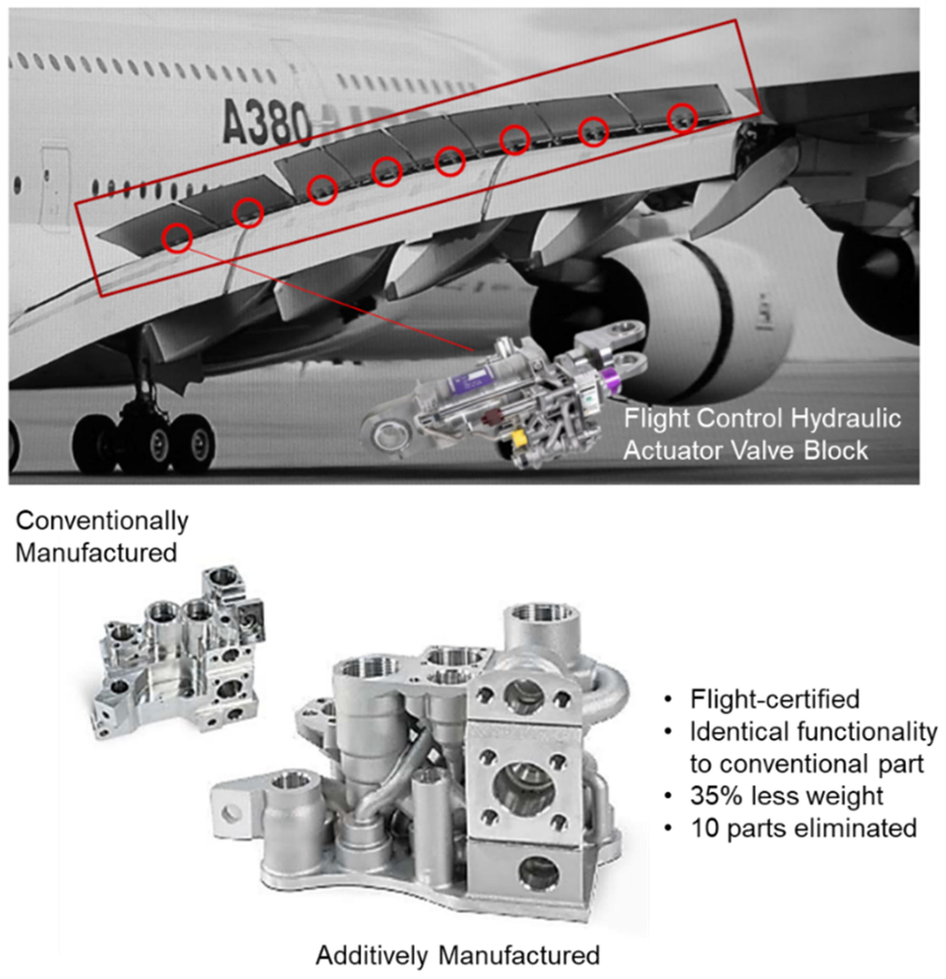
  74. EOS. First Metal 3D Printed Primary Flight Control Hydraulic Component Flies on an Airbus A380; EOS GmbH: Krailing/Munich, Germany, 2018. [Google Scholar]
  75. Khajavi, S.H.; Holmström, J.; Partanen, J. Additive Manufacturing in the Spare Parts Supply Chain: Hub Configuration and Technology Maturity. Rapid Prototyp. J. 2018, 24, 1178–1192. [Google Scholar] [CrossRef]
  76. ASTM 52900(2021); Additive Manufacturing—General Principles—Fundamentals and Vocabulary. ASTM International ISO: Geneva, Switzerland, 2022.
  77. Hybrid Manufacturing Technologies 7 Families of Additive Manufacturing. Available online: https://hybridmanutech.com/resources/ (accessed on 29 May 2023).
  78. Larikov, L.N.; Ivanov, M.A.; Nikitin, B.G. The Effect of Impurities and Crystal Structure Defects on Copper Heat Conduction at Low Temperatures. Phys. Status Solidi 1973, 19, 135–145. [Google Scholar] [CrossRef]
  79. Galsin, J.S. Physical Effects of Impurities in Metals. In Impurity Scattering in Metallic Alloys, 1st ed.; Springer: New York, NY, USA, 2002; pp. 93–123. [Google Scholar] [CrossRef]
  80. Mackey, P.J.; Wraith, A.E. Development of Copper Quality: An Historical Perspective. Trans. Institutions Min. Metall. Sect. C Miner. Process. Extr. Metall. 2004, 113, 25–37. [Google Scholar] [CrossRef]
  81. Kato, M. The Production of Ultrahigh-Purity Copper for Advanced Applications. Jom 1995, 47, 44–46. [Google Scholar] [CrossRef]
  82. EOS Copper Cu for EOS M 290. Available online: https://www.eos.info/03_system-related-assets/material-related-contents/metal-materials-and-examples/metal-material-datasheet/copper/material_datasheet_eos_copper_cu_core_en.pdf (accessed on 16 March 2023).
  83. Renishaw Additive Manufacturing of Intricate Structures in Commercially Pure Copper. Available online: https://www.renishaw.com/media/doc/en/45cb1a9524454c8ca0689dc953949222.docx (accessed on 16 March 2023).
  84. 3D Systems Oxygen-Free Copper (A). Available online: https://www.3dsystems.com/materials/oxygen-free-copper-a (accessed on 14 March 2023).
  85. GE Additive Arcam EBM Pure Copper. Available online: https://www.ge.com/additive/sites/default/files/2021-05/ArcamEBMPureCopperMDS_Q10plus-v2.0.pdf (accessed on 16 March 2023).
  86. Desktop Metal BMD-MDS-COPPER-201203. Available online: https://www.desktopmetal.com/uploads/BMD-SPC-MDS_Copper-201203.a.pdf (accessed on 16 March 2023).
  87. Desktop Metal SPJ-SPC-MDS-PureCu-211213. Available online: https://www.desktopmetal.com/uploads/SPJ-SPC-MDS-PureCu-211213_e.pdf (accessed on 16 March 2023).
  88. Markforged Material Datasheet Copper. Available online: https://www-objects.markforged.com/craft/materials/Copper-V1.1.pdf (accessed on 16 March 2023).
  89. Holo Team High Purity 3D Printed Copper Drives High Performance Metal Parts. Available online: https://holoam.com/blog/high-purity-drives-high-performance-3d-printed-copper (accessed on 12 June 2023).
  90. Wu, Z.; Narra, S.P.; Rollett, A. Exploring the Fabrication Limits of Thin-Wall Structures in a Laser Powder Bed Fusion Process. Int. J. Adv. Manuf. Technol. 2020, 110, 191–207. [Google Scholar] [CrossRef]
  91. Calignano, F.; Cattano, G.; Manfredi, D. Manufacturing of Thin Wall Structures in AlSi10Mg Alloy by Laser Powder Bed Fusion through Process Parameters. J. Mater. Process. Technol. 2018, 255, 773–783. [Google Scholar] [CrossRef]
  92. Algardh, J.K.; Horn, T.; West, H.; Aman, R.; Snis, A.; Engqvist, H.; Lausmaa, J.; Harrysson, O. Thickness Dependency of Mechanical Properties for Thin-Walled Titanium Parts Manufactured by Electron Beam Melting (EBM) ®. Addit. Manuf. 2016, 12, 45–50. [Google Scholar] [CrossRef]
  93. Kiani, P.; Dupuy, A.D.; Ma, K.; Schoenung, J.M. Directed Energy Deposition of AlSi10Mg: Single Track Nonscalability and Bulk Properties. Mater. Des. 2020, 194, 108847. [Google Scholar] [CrossRef]
  94. Bhatt, P.M.; Malhan, R.K.; Rajendran, P.; Gupta, S.K. Building Free-Form Thin Shell Parts Using Supportless Extrusion-Based Additive Manufacturing. Addit. Manuf. 2020, 32, 101003. [Google Scholar] [CrossRef]
  95. Bhuvanesh Kumar, M.; Sathiya, P. Methods and Materials for Additive Manufacturing: A Critical Review on Advancements and Challenges. Thin-Walled Struct. 2021, 159, 107228. [Google Scholar] [CrossRef]
  96. Guan, J.; Zhang, X.; Jiang, Y.; Yan, Y. Insights into Fabrication Mechanism of Pure Copper Thin Wall Components by Selective Infrared Laser Melting. Rapid Prototyp. J. 2019, 25, 1388–1397. [Google Scholar] [CrossRef]
  97. Matthews, M.J.; Guss, G.; Khairallah, S.A.; Rubenchik, A.M.; Depond, P.J.; King, W.E. Denudation of Metal Powder Layers in Laser Powder Bed Fusion Processes. Acta Mater. 2016, 114, 33–42. [Google Scholar] [CrossRef]
  98. Shi, W.; Wang, P.; Liu, Y.; Han, G. Experiment of Process Strategy of Selective Laser Melting Forming Metal Nonhorizontal Overhanging Structure. Metals 2019, 9, 385. [Google Scholar] [CrossRef]
  99. Silbernagel, C.; Gargalis, L.; Ashcroft, I.; Hague, R.; Galea, M.; Dickens, P. Electrical Resistivity of Pure Copper Processed by Medium-Powered Laser Powder Bed Fusion Additive Manufacturing for Use in Electromagnetic Applications. Addit. Manuf. 2019, 29, 100831. [Google Scholar] [CrossRef]
  100. Kaden, L.; Matthäus, G.; Ullsperger, T.; Engelhardt, H.; Rettenmayr, M.; Tünnermann, A.; Nolte, S. Selective Laser Melting of Copper Using Ultrashort Laser Pulses. Appl. Phys. A Mater. Sci. Process. 2017, 123, 596. [Google Scholar] [CrossRef]
  101. Kaden, L.; Seyfarth, B.; Ullsperger, T.; Matthäus, G.; Nolte, S. Selective Laser Melting of Copper Using Ultrashort Laser Pulses at Different Wavelengths. In Laser 3D Manufacturing V; Helvajian, H., Piqué, A., Gu, B., Eds.; SPIE: Bellingham, WA, USA, 2018; Volume 1052312, p. 41. [Google Scholar]
  102. Kaden, L.; Matthäus, G.; Ramm, R.; Ullsperger, T.; Seyfarth, B.; Nolte, S. Additive Manufacturing of Pure Copper Using Ultrashort Laser Pulses. In Laser 3D Manufacturing VI; Helvajian, H., Gu, B., Chen, H., Eds.; SPIE: Bellingham, WA, USA, 2019; p. 12. [Google Scholar]
  103. Ma, Z.X.; Ning, J.; Yu, B.; Zhang, L.J.; Fan, J.H.; Yuan, L.G. Effects of Process Parameters and Scanning Patterns on Quality of Thin-Walled Copper Flanges Manufactured by Selective Laser Melting. J. Manuf. Process. 2021, 72, 419–430. [Google Scholar] [CrossRef]
  104. Jadhav, S.D.; Goossens, L.R.; Kinds, Y.; Van Hooreweder, B.; Vanmeensel, K. Laser-Based Powder Bed Fusion Additive Manufacturing of Pure Copper. Addit. Manuf. 2021, 42, 101990. [Google Scholar] [CrossRef]
  105. Zhang, L.-J.; Zhang, G.-F.; Ning, J.; Zhang, X.-J.; Zhang, J.-X. Microstructure and Properties of the Laser Butt Welded 1.5-Mm Thick T2 Copper Joint Achieved at High Welding Speed. Mater. Des. 2015, 88, 720–736. [Google Scholar] [CrossRef]
  106. Bayat, M.; Thanki, A.; Mohanty, S.; Witvrouw, A.; Yang, S.; Thorborg, J.; Tiedje, N.S.; Hattel, J.H. Keyhole-Induced Porosities in Laser-Based Powder Bed Fusion (L-PBF) of Ti6Al4V: High-Fidelity Modelling and Experimental Validation. Addit. Manuf. 2019, 30, 100835. [Google Scholar] [CrossRef]
  107. Laser 2000 Blue High Power Diode Laser with 200 W for Material Processing. Available online: https://www.laser2000.com/fr/en/lasers/31701-blue-high-power-diode-laser-with-200-w-for-material-processing.html (accessed on 21 June 2023).
  108. Qu, S.; Ding, J.; Fu, J.; Fu, M.; Zhang, B.; Song, X. High-Precision Laser Powder Bed Fusion Processing of Pure Copper. Addit. Manuf. 2021, 48, 102417. [Google Scholar] [CrossRef]
  109. Gruber, S.; Stepien, L.; López, E.; Brueckner, F.; Leyens, C. Physical and Geometrical Properties of Additively Manufactured Pure Copper Samples Using a Green Laser Source. Materials 2021, 14, 3642. [Google Scholar] [CrossRef]
  110. Hori, E.; Sato, Y.; Shibata, T.; Tojo, K.; Tsukamoto, M. Development of SLM Process Using 200 W Blue Diode Laser for Pure Copper Additive Manufacturing of High Density Structure. J. Laser Appl. 2021, 33, 012008. [Google Scholar] [CrossRef]
  111. Nordet, G.; Gorny, C.; Mayi, Y.; Daligault, J.; Dal, M.; Effernelli, A.; Blanchet, E.; Coste, F.; Peyre, P. Absorptivity Measurements during Laser Powder Bed Fusion of Pure Copper with a 1 KW Cw Green Laser. Opt. Laser Technol. 2022, 147, 107612. [Google Scholar] [CrossRef]
  112. Horn, M.; Schmitt, M.; Schafnitzel, M.; van Husen, A.; Wagenblast, P.; Auernhammer, S.; Heyder, J.; Hauck, C.; Barz, J.; Ott, M.; et al. Powder Bed Fusion of Highly Filigree Copper Features Using a Green Laser. Procedia CIRP 2022, 111, 81–86. [Google Scholar] [CrossRef]
  113. Takenaka, K.; Sato, Y.; Yoshida, N.; Yoshitani, M.; Heya, M.; Tsukamoto, M. Additive Manufactured of Pure Copper by Blue Diode Laser Induced Selective Laser Melting. J. Laser Appl. 2022, 34, 042041. [Google Scholar] [CrossRef]
  114. Johnson, K.; Burden, E.; Shaffer, M.; Noack, T.; Mueller, M.; Walker, J.; MacDonald, E.; Cortes, P.; Quintana, J. A Copper Pyramidal Fractal Antenna Fabricated with Green-Laser Powder Bed Fusion. Prog. Addit. Manuf. 2022, 7, 931–942. [Google Scholar] [CrossRef]
  115. Yan, X.; Wang, C.; Xiong, W.; Hou, T.; Hao, L.; Tang, D. Thermal Debinding Mass Transfer Mechanism and Dynamics of Copper Green Parts Fabricated by an Innovative 3D Printing Method. RSC Adv. 2018, 8, 10355–10360. [Google Scholar] [CrossRef] [PubMed]
  116. Schoen, A.H. Infinite Periodic Minimal Surfaces without Self-Intersections; NASA TN D-5541; NASA Electronics Research Centre Cambridge: Cambridge, MA, USA, 1970. Available online: https://ntrs.nasa.gov/api/citations/19700020472/downloads/19700020472.pdf (accessed on 21 June 2023).
  117. Protolabs An Intro to Metal Additive Manufacturing with DMLS. Available online: https://www.protolabs.com/resources/blog/an-intro-to-metal-additive-manufacturing-with-dmls/%0A (accessed on 21 June 2023).
  118. Pérez, M.; García-Collado, A.; Carou, D.; Medina-Sánchez, G.; Dorado-Vicente, R. On Surface Quality of Engineered Parts Manufactured by Additive Manufacturing and Postfinishing by Machining. In Additive Manufacturing; Elsevier: Amsterdam, The Netherlands, 2021; pp. 369–394. ISBN 9780128184110. [Google Scholar]
  119. Takenaka, K.; Sato, Y.; Tojo, K.; Tsukamoto, M. Development of SLM 3D Printing System Using Galvano Scanner for Pure Copper Additive Manufacturing by 200 W Blue Diode Laser. In Proceedings of the Lasers in Manufacturing, online virtual event, 21–24 June 2021. [Google Scholar]
  120. Kang, S.; Gainov, R.; Heußen, D.; Bieler, S.; Sun, Z.; Weinberg, K.; Dehm, G.; Ramachandramoorthy, R. Green Laser Powder Bed Fusion Based Fabrication and Rate-Dependent Mechanical Properties of Copper Lattices. Mater. Des. 2023, 231, 112023. [Google Scholar] [CrossRef]
  121. Alphonso, W.E.; Bayat, M.; Hattel, J. Comparison between green and infrared laser in laser powder bed fusion of pure copper through high fidelity numerical modelling at meso-scale. In Proceedings of the International Seminar on Numerical Analysis of Weldability, Graz, Austria, 4–7 September 2022. [Google Scholar]
  122. Bishara, H.; Lee, S.; Brink, T.; Ghidelli, M.; Dehm, G. Understanding Grain Boundary Electrical Resistivity in Cu: The Effect of Boundary Structure. ACS Nano 2021, 15, 16607–16615. [Google Scholar] [CrossRef]
  123. Romano, T.; Migliori, E.; Mariani, M.; Lecis, N.; Vedani, M. Densification Behaviour of Pure Copper Processed through Cold Pressing and Binder Jetting under Different Atmospheres. Rapid Prototyp. J. 2022, 28, 1023–1039. [Google Scholar] [CrossRef]
  124. Bai, Y.; Williams, C.B. An Exploration of Binder Jetting of Copper. Rapid Prototyp. J. 2015, 21, 177–185. [Google Scholar] [CrossRef]
  125. Kumar, A.; Bai, Y.; Eklund, A.; Williams, C.B. Effects of Hot Isostatic Pressing on Copper Parts Fabricated via Binder Jetting. Procedia Manuf. 2017, 10, 935–944. [Google Scholar] [CrossRef]
  126. Bai, Y.; Wagner, G.; Williams, C.B. Effect of Particle Size Distribution on Powder Packing and Sintering in Binder Jetting Additive Manufacturing of Metals. J. Manuf. Sci. Eng. Trans. ASME 2017, 139, 081019. [Google Scholar] [CrossRef]
  127. Bai, Y.; Williams, C.B. The Effect of Inkjetted Nanoparticles on Metal Part Properties in Binder Jetting Additive Manufacturing. Nanotechnology 2018, 29, 395706. [Google Scholar] [CrossRef] [PubMed]
  128. Bai, Y.; Williams, C.B. Binder Jetting Additive Manufacturing with a Particle-Free Metal Ink as a Binder Precursor. Mater. Des. 2018, 147, 146–156. [Google Scholar] [CrossRef]
  129. Yegyan Kumar, A.; Wang, J.; Bai, Y.; Huxtable, S.T.; Williams, C.B. Impacts of Process-Induced Porosity on Material Properties of Copper Made by Binder Jetting Additive Manufacturing. Mater. Des. 2019, 182, 108001. [Google Scholar] [CrossRef]
  130. Moritzer, E.; Elsner, C.L. Investigation and Improvement of Processing Parameters of a Copper-Filled Polymer Filament in Fused Filament Fabrication as a Basis for the Fabrication of Low-Porosity Metal Parts. Macromol. Symp. 2022, 404, 2100390. [Google Scholar] [CrossRef]
  131. Singh, G.; Missiaen, J.-M.; Bouvard, D.; Chaix, J.-M. Copper Additive Manufacturing Using MIM Feedstock: Adjustment of Printing, Debinding, and Sintering Parameters for Processing Dense and Defectless Parts. Int. J. Adv. Manuf. Technol. 2021, 115, 449–462. [Google Scholar] [CrossRef]
  132. Ji, X.; Xu, J.; Abanda, A.M. Copper Foam Based Vapor Chamber for High Heat Flux Dissipation. Exp. Therm. Fluid Sci. 2012, 40, 93–102. [Google Scholar] [CrossRef]
  133. Shirazy, M.R.S.; Fréchette, L.G. Capillary and Wetting Properties of Copper Metal Foams in the Presence of Evaporation and Sintered Walls. Int. J. Heat Mass Transf. 2013, 58, 282–291. [Google Scholar] [CrossRef]
  134. Yang, H.; Yang, Y.; Ma, B.; Zhu, Y. Experimental Study on Capillary Microflows in High Porosity Open-Cell Metal Foams. Micromachines 2022, 13, 2052. [Google Scholar] [CrossRef]
  135. Advanced Cooling Technologies Heat Pipe Wick Properties. Available online: https://www.1-act.com/resources/heat-pipe-resources/heat-pipe-wicks/heat-pipe-wick-properties/ (accessed on 18 June 2023).
  136. Singh, A.; Caprio, L.; Previtali, B.; Demir, A.G. Processability of Pure Cu by LPBF Using a Ns-Pulsed Green Fiber Laser. Opt. Laser Technol. 2022, 154, 108310. [Google Scholar] [CrossRef]
  137. Miyanaji, H.; Ma, D.; Atwater, M.A.; Darling, K.A.; Hammond, V.H.; Williams, C.B. Binder Jetting Additive Manufacturing of Copper Foam Structures. Addit. Manuf. 2020, 32, 100960. [Google Scholar] [CrossRef]
  138. ASTM F3184-16; Standard Specification for Additive Manufacturing Stainless Steel Alloy (UNS S31603) with Powder Bed Fusion. ASTM International: West Conshehoken, PA, USA, 2016.
  139. ASTM F3055-14a(2021); Standard Specification for Additive Manufacturing Nickel Alloy (UNS N07718) with Powder Bed Fusion. ASTM International: West Conshehoken, PA, USA, 2021. [CrossRef]
  140. ASTM F3318-18; Standard for Additive Manufacturing—Finished Part Properties—Standard Specification for Titanium Alloys via Powder Bed Fusion. ASTM International: West Conshehoken, PA, USA, 2018. [CrossRef]
  141. ASTM F2924-14(2021); Standard Specification for Additive Manufacturing Titanium-6 Aluminum-4 Vanadium with Powder Bed Fusion. ASTM International: West Conshehoken, PA, USA, 2021. [CrossRef]
  142. ASTM F3001-14(2021); Standard Specification for Additive Manufacturing Titanium-6 Aluminum-4 Vanadium ELI (Extra Low Interstitial) with Powder Bed Fusion. ASTM International: West Conshehoken, PA, USA, 2021. [CrossRef]
Figure 1. Exposed internal channels of a cold plate heat sink fabricated via (a) additive manufacturing [1] and (b) conventional machining [2].
Technologies 11 00141 g001
Figure 2. Coating damages to the optical mirror (denoted by dotted outline) of a laser-powder bed fusion printer after being subjected to a 12 h exposure to back-reflections from a bulk copper substrate [15].
Technologies 11 00141 g002
Figure 4. Numerical modelling comparisons of lattice structures (Gyroid and Schwarz-D) against a reference printed circuit heat exchanger (PCHE) with linear channel geometries for their (a) computational fluid domains, (b) specific heat transfer surface areas, and (c) heat transfer performances quantified by Nusselt number (Nu) at various pumping powers [56].
Technologies 11 00141 g004
Figure 5. (a) Topology-optimised solutions for the most effective heat dissipation geometries in natural convection heat sinks over the range of 103 < Grashof number Gr < 106, and (b) solution evolution for Grashof number Gr = 106 up to 1000 iterations [62].
Technologies 11 00141 g005
Figure 6. Integrated heat pipe wick with hierarchical micro-porous structure and grooved channels [63].
Technologies 11 00141 g006
Figure 7. Surfaces of porous nickel heat pipe wick: (a) in original as-sintered condition, (b) after lathing, and (c) after wire-electric discharge machining (wire-EDM). Pores were crushed or blocked and ligaments damaged after lathing or wire-EDM, which inhibited capillary flow of working fluid [68].
Technologies 11 00141 g007
Figure 8. Differences in the range of electric vehicles at freezing and near room temperatures [70].
Technologies 11 00141 g008
Figure 9. AM hydraulic valve block jointly developed by Liebherr-Aerospace and EOS [74].
Technologies 11 00141 g009
Figure 10. Seven families of additive manufacturing technologies [77].
Technologies 11 00141 g010
Figure 11. Thermal conductivities of 4N and 6N copper can differ by up to an order of magnitude at low temperatures [81].
Technologies 11 00141 g011
Figure 12. Copper components fabricated using Laser Powder Bed Fusion AM. (a) Heat sink, source: Renishaw, (b) TPMS gyroid structure with 0.35 mm wall thickness and 5 mm cell size, source: Renishaw, (c) heat exchanger, source: EOS, (d) heat exchanger, source: Delva Oy, and (e) heat exchanger, source: 3D Systems.
Technologies 11 00141 g012
Figure 13. (a) Pure copper thin-wall grid structures with wall thickness of 0.2 mm, 0.3 mm, and 0.5 mm fabricated using NIR L-PBF [96], (b) meander exposure strategy for three consecutive layers N, N+1, and N+2 [98], (c) close-up optical image of grid structure shown in (a) with porous surface texture [96], (d) SEM image of grid structure with lack-of-fusion resulting in individual meltpool beads [96], and (e) SEM image of grid structure node intersection, with trapped spherical particles within cave-like pores [96].
Technologies 11 00141 g013
Figure 14. (a) Free-standing pure copper thin walls fabricated via NIR L-PBF at various laser powers, scan speeds, and layer thicknesses, (b) cross-section of thin walls illustrating bulging at the base, and (c) EDX analysis of cross-section highlighting iron contamination at the base causing the bulging [99].
Technologies 11 00141 g014
Figure 15. (a) Pure copper thin-wall structures fabricated using ultrashort pulse L-PBF [100], (b) SEM image of thin-wall structure displaying wall thickness of 100 µm and homogeneous high porosity [100], (c,d) pure copper thin-wall structures fabricated using ultrashort pulse L-PBF at 1030 nm (NIR) and 515 nm (green) wavelengths [101], (e,f) corresponding SEM images to (c,d) showing the highly similar structures produced [101], (g) topology-optimised structure for a lightweight mirror mount [102], (h) turbine wheel with highly inclined overhanging thin fins not requiring support structures [102], and (i) thin-wall structure with 100 µm wall thickness and extremely high aspect ratio of 70:1 [102].
Technologies 11 00141 g015
Figure 16. (a) Influence of using higher NIR laser powers up to 500 W for various scan speeds and hatching distances on relative density, surface roughness, and wall thickness, (b) resulting copper flanges fabricated from process parameters shown in (a), (c) main effect plots for laser power, scan speed, and hatching distance on relative density, (d) schematic of linear scanning and circular scanning exposure strategies, and (e) comparison of wall thickness, surface roughness, and relative density for linear and circular scanning exposure strategies [103].
Technologies 11 00141 g016
Figure 17. (a) Porosity analysis images of bulk copper specimens fabricated using NIR L-PBF between 200 W and 500 W for various scan speeds, with green dotted outline representing ideal keyhole regime with good fusion, blue dotted outline representing keyhole-induced porosity regime, and red outline representing lack-of-fusion conduction regime, (b) schematics of conduction, keyhole, and keyhole-induced porosity regimes in L-PBF of pure copper, (c) mapping of keyhole regime, conduction regime, and transition zone between regimes to laser power and scan speed [104].
Technologies 11 00141 g017
Figure 18. Absorption of metals at different irradiation wavelengths [107].
Technologies 11 00141 g018
Figure 19. (a) Schematic of single-line exposure strategy used to fabricate thin walls, (b) free-standing thin walls fabricated using a bespoke high precision NIR L-PBF at various laser powers and scan speeds, (c) processing windows for lack of fusion, densification, and overfusion, (d) close up of side and top surfaces of thin walls for different processing windows, as indicated, (e) top and side surface roughness of thin walls for different processing windows, and (f) meltpool width and depth for different processing windows [108].
Technologies 11 00141 g019
Figure 20. Comparison of meltpool bead size between NIR and short-wavelength blue lasers with same beam spot size at different scan speeds [110].
Technologies 11 00141 g020
Figure 21. (a) Design of thin-wall specimen coupons for fabrication with a continuous wavelength green laser [112], (b) cross-section of thin walls consisting of a dense core region with porous branch-like structures of solidified melt beads [112], (c) wall thickness of thin walls fabricated using different number of scan tracks at print angles of 90° (vertical), 60°, and 30° [112], and (d) similar dense core/porous outer shell phenomena is observed in another study when green lasers are used [109].
Technologies 11 00141 g021
Figure 22. Comparison of thin-wall fabrication capabilities of NIR lasers [103] and green lasers [112].
Technologies 11 00141 g022
Figure 23. (a) Workflow of paste material extrusion method, (b) vase-like geometry formed using material extrusion with smooth walls of 340 µm wall thickness, and (c) EDX analysis indicates no carbon residue after pyrolysis, but some amount of oxygen is detected [115].
Technologies 11 00141 g023
Figure 24. (a) Extremely high resolution of small components fabricated using digital light processing (vat photopolymerisation) of a copper slurry, and (b) wall thickness as low as 100 µm with visually high geometrical stability and smooth surfaces [89].
Technologies 11 00141 g024
Figure 25. (a) Increased deformation and overheating at high inclination angles for overhangs [117], and (b) staircase effect of inclined or curved surfaces [118].
Technologies 11 00141 g025
Figure 26. (a) N14 and primitive-type lattice structures fabricated using a high precision NIR L-PBF printer, (b) cross-sectional area of vertical lattice wall shows good densification, smooth surfaces, and a thickness of 100 µm (c) comparison of wall thickness for top and side surfaces, (d) comparison of surface roughness for top and side surfaces, and (e) schematic illustrating laser burn-through and over-penetration for highly inclined surfaces [108].
Technologies 11 00141 g026
Figure 27. Larger minimum unit cell size, lower resolution, and rougher surfaces in lattice structures produced using a (a) blue laser [119] and (b) green laser [120] in L-PBF.
Technologies 11 00141 g027
Figure 28. The narrow processing windows of pure copper for NIR lasers in L-PBF can result in unstable meltpools and distorted geometry (red outline) compared to green lasers with larger processing windows [121].
Technologies 11 00141 g028
Figure 29. Complex triply periodic minimal surface lattice structures with high resolution and smooth homogeneous surfaces using digital light processing (vat photopolymerisation). Source: Holo.
Technologies 11 00141 g029
Figure 30. (a) Bulk pure copper foam structures fabricated using ultrashort pulse L-PBF with a green femtosecond laser [102], (b) horizontal planar view of (a) [102], (c) vertical planar view of (a) [102], (d) 3D view of copper foam fabricate using ultrashort pulse L-PBF as observed via SEM [101], (e) bulk pure copper foam fabricated using ultrashort pulse L-PBF with a nanosecond green laser [136], and (f) porosity levels at various laser powers and scan speeds [136].
Technologies 11 00141 g030
Figure 31. (a) Schematic of Additive Expansion by the Reduction of Oxides (AERO) process, and (b) SEM image of copper foam produced using AERO process.
Technologies 11 00141 g031
Table 1. List of structural metals in order of decreasing thermal conductivity at temperatures between 0 °C and 25 °C [9].
Material Thermal   Conductivity   ( W / m K)
Aluminium236
High Carbon Steel36
Titanium22
Inconel Nickel Alloy15
304 Stainless Steel14
Table 2. Comparison of TPMS lattice structures in heat exchangers to conventional designs. Modified from [59].
Reference (Year)Experimental MethodWorking Fluid (Hot/Cold)TPMS Structure(s) InvestigatedKey Findings
Femmer et al. (2015) [60]Empirical (Nusselt number, Nu) and Computation Fluid Dynamics (Pressure Drop, Δ P )Water-Water
  • Schwarz-P (P), Schwarz-D (D), Gyroid (G), I-graph-wrapped package (IWP)
  • 5 × 5 × 5 unit cell configuration in a 10 × 10 × 10 mm3 volume
  • 0.4 mm wall thickness
  • Overall, TPMS structures perform better than their conventional design counterparts (plate and tube) in terms of Nusselt number, in the order NuTPMS > NuPlate > NuTube;
  • For a flow rate above 12 mL/min, the relative heat transfer performance of TPMS structures are NuD > NuIWP > NuG > NuP, which is in the same order of the available surface area for heat exchange from the different TPMS structures, respectively;
  • The pressure drop performance of the tested designs from smallest (best) to highest (worst) are Δ P T u b e < Δ P P < Δ P G < Δ P D < Δ P I W P ;
  • To provide a singular metric to evaluate heat transfer performance against pressure drop, the “surface area goodness factor” N u / P r 1 3 ω was used, and all TPMS structures except P were found to perform better than the conventional tube design;
  • In fact, P performed equivalently to the conventional tube design;
  • D exhibits the best heat transfer to pressure drop performance.
Peng et al. (2019) [61]Computational Fluid DynamicsWater-Water
  • Gyroid (G)
  • 10 × 10 × 10 mm3 unit cells
  • 0.5 mm wall thickness
  • G has more than twice the available surface area for heat exchange (251.5 cm2) compared to the reference plate type heat exchanger with straight channels (120 cm2) for the same bulk volume;
  • At a flow velocity of 10 mm/s, the TPMS heat exchanger has 6× the heat transfer rate of the reference heat exchanger at the expense of 14× the pressure drop;
  • At a flow velocity of 20 mm/s, the TPMS heat exchanger has 7.5× the heat transfer rate of the reference heat exchanger at the expense of 19× the pressure drop;
  • Regardless, the absolute value of the maximum pressure drop for the TPMS heat exchanger at 19 Pa (0.000188 atm) is trivial in exchange for an absolute increase in heat transfer rate by 1 KW compared to the reference heat exchanger.
Li et al. (2020) [56]Computational Fluid DynamicsSupercritical CO2-Supercritical CO2
  • Schwarz-D (D), Gyroid (G)
  • 3.77 × 3.77 × 24 mm3 fluid domains
  • 1.61 mm hydraulic diameter
  • 0.7 mm wall thickness
  • Both D and G produce up to two orders of magnitude higher turbulent kinetic energy than the reference printed circuit heat exchanger (PCHE) with linear channels;
  • In particular, G produces the highest turbulent kinetic energy due to strong flow mixing in the interconnected channels;
  • Both D and G produce a higher heat transfer coefficient than the reference PCHE from 16–120% depending on the flow regime governed by Reynolds number;
  • After factoring in pressure drop, both D and G outperform the PCHE by 17–100% in overall thermal performance.
Table 3. Manufacturer-specified properties of commercially available high-purity copper AM solutions (as of September 2023).
CategoryAM
Process 1
AM Solution ProviderEquipmentCopper Feedstock Purity
(%)
Layer Thickness (µm)Relative
Density 2 (%)
Electrical Conductivity
(% IACS 3)
Thermal Conductivity 4
( W / m · K )
Yield Strength (MPa)Tensile Strength
(MPa)
Elongation at Break
(%)
Surface Roughness (µm)Minimum Wall Thickness Demonstrated (mm)Ref.
Beam-BasedL-PBFEOSM 290
(400 W version)
-20>95>80
(as printed)
>90
(heat treated)
>332
(as printed)
>373
(heat treated)
180
(as printed)
140
(heat treated)
200
(as printed)
190
(heat treated)
5
(as printed)
20
(heat treated)
--[82]
M 290
(1 kW version)
99.9540>99.3100.7
(as printed)
418
(as printed)
159–162
(as printed)
227–230
(as printed)
45.6–48.1
(as printed)
Sa 10–15
(Z-direction)
0.7[11]
TRUMPFTruPrint 1000 (Green Edition)
TruPrint 5000
(Green Edition)
>99.9->99.5100415-----[12,13]
RenishawRenAM 500S99.930>98------0.35[83]
3D SystemsDMP 350 variants-->99.5102
(as printed)
423
(as printed)
-----[84]
EBMGE AdditiveArcam Q10plus v2.0>99.9550->98
(as printed)
>406
(as printed)
105–125
(as printed)
170–200
(as printed)
31–35
(as printed)
--[85]
Sinter-BasedBJTDesktop MetalStudio System99.9->97.685.2
(as sintered)
353
(as sintered)
45
(as sintered)
195
(as sintered)
37
(as sintered)
--[86]
Production System P-1 and P-50>99.95-96.590
(as sintered)
373
(as sintered)
37
(as sintered)
174
(as sintered)
28
(as sintered)
Ra 3–12
(top and Z-direction)
-[87]
FFFMarkforgedMetal X>99.8-9884
(as sintered)
350
(as sintered)
26
(as sintered)
117–193
(as sintered)
15–45
(as sintered)
--[88]
VPPHoloPureForm99.9-9592366----0.1[89]
1 L-PBF—Laser Powder Bed Fusion; EBM—Electron Beam Melting; BJT—Binder Jetting; FFF—Fused Filament Fabrication; VPP—Vat Photopolymerisation. 2 Relative density that is expressed as a percentage of solid bulk pure copper at 8.96 g/cm3. 3 IACS—International Annealed Copper Standard, 100% IACS corresponds to an electrical conductivity of 58 MS/m at 20 °C. 4 Other than Markforged and Holo, all thermal conductivity values in this table have not been specified by their respective AM solution providers and are calculated from electrical conductivity using Wiedemann–Franz Law.
Table 4. Key examples in state-of-the-art 3 D printing of pure copper filigree structures.
TechnologyBeam-Based AMSinter-Based AM
AM Process 1L-PBFMEXVPPBJT
Laser CharacteristicsNear-Infrared (1060 nm)Short-Wavelength (515–650 nm)PulsedNA
Low PowerMedium PowerGreen (515 nm)Blue (650 nm)Near Infrared (1060 nm)Green (515 nm)
Reference[108][103][112][110][100,101,102][115][89][137]
Laser Power (W)200400200–5002002411NA
Beam Spot Diameter (µm)25502002003530
Type of Filigree Structures FabricatedHigh-Density Thin WallsBulk Foams and Thin-Wall FoamsHigh-Density Thin WallsBulk Foams
Minimum Wall Thickness (µm)150126300550<100<100340100NA
Relative Density 2 (%) of filigree structure fabricated, or otherwise as describedVisually dense and pore-free cross-section99.86Visually dense core surrounded by porous protrusions of melt beadsNA for thin wall; bulk material relative density of 99.1%Highly porous and homogeneous cross-sectionHighly porous and homogeneous cross-section90.4NA for thin wall; bulk material relative density of 95%41
Surface Roughness (µm) of filigree structure fabricated, or otherwise as describedRa < 515Visually rough due to protruding melt beadsVisually rough due to high porosityVisually smoothVisually smoothVisually rough due to high porosity
1 L-PBF—Laser Powder Bed Fusion; MEX—Material Extrusion; VPP—Vat Photopolymerisation; BJT—Binder Jetting; 2 Relative density that is expressed as a percentage of solid bulk pure copper at 8.96 g/cm3..
Disclaimer/Publisher’s Note: The statements, opinions and data contained in all publications are solely those of the individual author(s) and contributor(s) and not of MDPI and/or the editor(s). MDPI and/or the editor(s) disclaim responsibility for any injury to people or property resulting from any ideas, methods, instructions or products referred to in the content.

