
Multi-Objective Comparative Analysis of Active Modular Rectifier Architectures for a More Electric Aircraft †

 ,
,  , , and
Abstract
:1. Introduction
2. Suitability of Active Rectifier Topologies in MEA
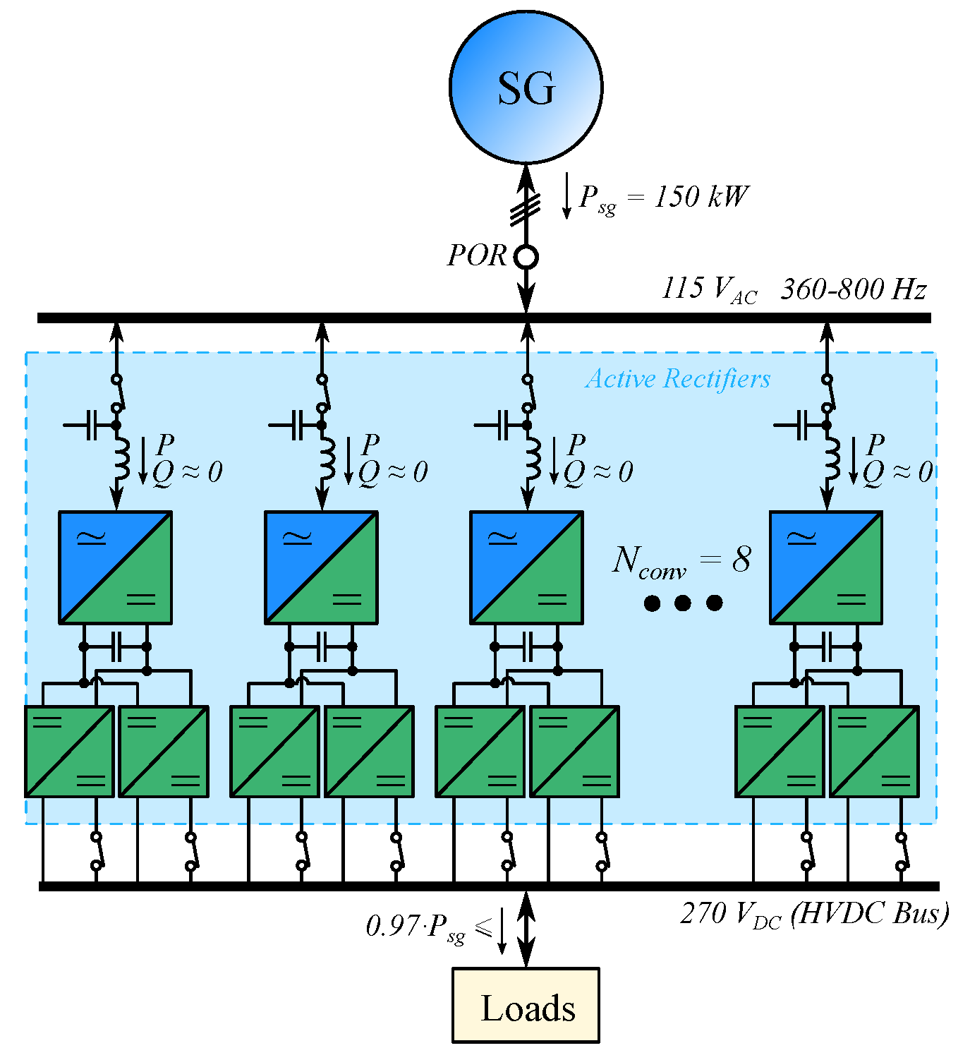
2.1. Application Requirements and Operating Scenario
2.2. Evaluation and Limitations of Active Rectifier Topologies
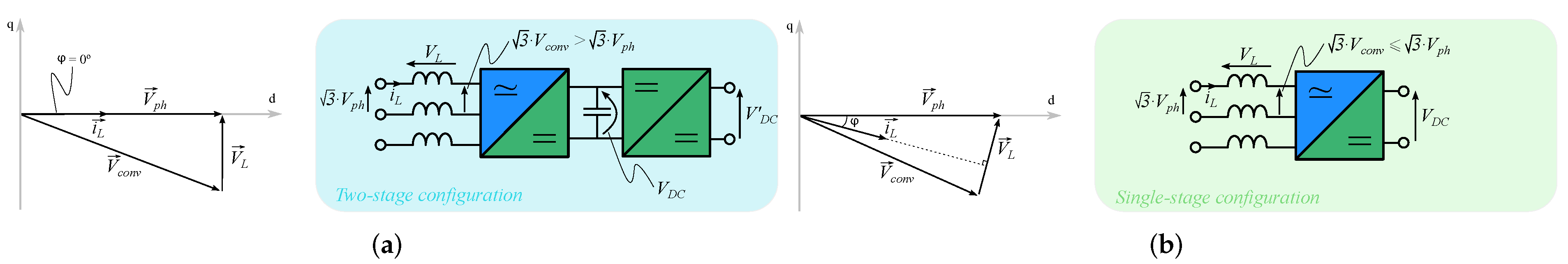
- 1.
- Two-stage configuration: considering the best PF operating condition case in Table 1, the active rectifier presents unity PF operation, and, according to the phasor diagram in Figure 2a, > . Thus, the rectifier output voltage (V > 282 V) does not fulfil the application requirements and a posterior DC/DC conversion is required to achieve the specified output 270 V, expressed as .
- 2.
- Single-stage configuration: considering the worst PF operating condition case in Table 1, the active rectifier performs at PF = 0.85 lagging and, therefore, ≤ condition is fulfilled, as depicted in Figure 2b. Therefore, no additional converter is required downstream for achieving the targeted 270 V.
2.3. Proposed Converter Configurations for Operating at Unity PF
3. Comparison Framework for Active Rectification Architectures
3.1. Efficiency Estimation
3.2. Volume Estimation
3.2.1. Cooling System Volume
- For safety reasons, the achievable maximum junction temperature was defined as 15 °C lower than the data sheet temperature and, hence, was limited to 185 °C.
- Water-cooling was assumed in order to achieve a high power density architecture. Based on the cooling system specifications of “IQ-evolution” [43], a temperature jump from heat sink to ambient, , of 15 °C is defined.
- An ambient temperature of 70 °C is assumed according to the worst case temperature in [30].
- Due to the high frequency of the SG voltage, the junction temperature ripple of the power semiconductor devices is negligible. Thus, instead of the transient impedances, only the thermal resistance is considered in this comparison.
3.2.2. Volume of the Passive Components
3.3. Reliability Estimation
3.3.1. Cosmic Ray Failure Rate
- A 50% for the power devices of the AC/DC stage;
- A 13.5% and 86.5% for the upper and down power devices in the DC/DC stage of 2L converter, respectively.
3.3.2. Wear-Out Performance Analysis
- The MOSFET lifetime model and the fitting parameters employed derived from testing data in [46];
- The thermal and electrical parameters related to the power devices, which could vary due to the manufacturing process and semiconductor technology; or
- The simplified mission profile, which could vary with the climate change and load conditions.
4. Converter Configuration and Architecture Design
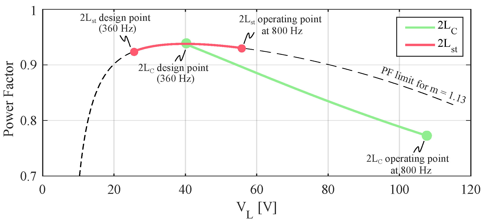
- The operating PF of the power converters were analyzed by the equation describing the phase diagrams in Figure 2, being,where refers to the operating PF; and, symbolizes the inductor RMS voltage, which can be expressed as,being, f the SG frequency in Table 1, the RMS current flowing through the input filter inductor, and, P the converter nominal power.We should note that, in the case of 2L and 2L single-stage configurations (PF < 1), the higher the operating PF, the lower the reactive power to be compensated and, hence, higher efficiency. If (1) and (13) are merged, the maximum operating PF of these topologies can be obtained depending on for a fixed m,
- Space vector pulse width modulation (SVPWM) pattern is assumed and a maximum m = 1.13 to ensure the minimum conduction and blocking times of the employed semiconductor.
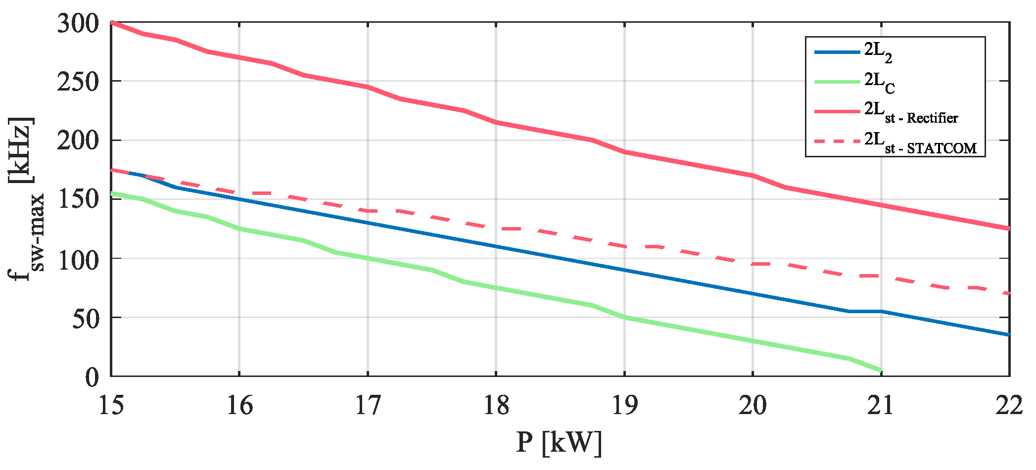
- The converter nominal power is defined by means of a thermal analysis based on the steady-state thermal model described in Section 3.2.1. This way, the maximum converter switching frequency is obtained depending on P while maintaining an efficiency result of ≥ 97%. The results of the thermal analysis are illustratively represented in Figure 6.
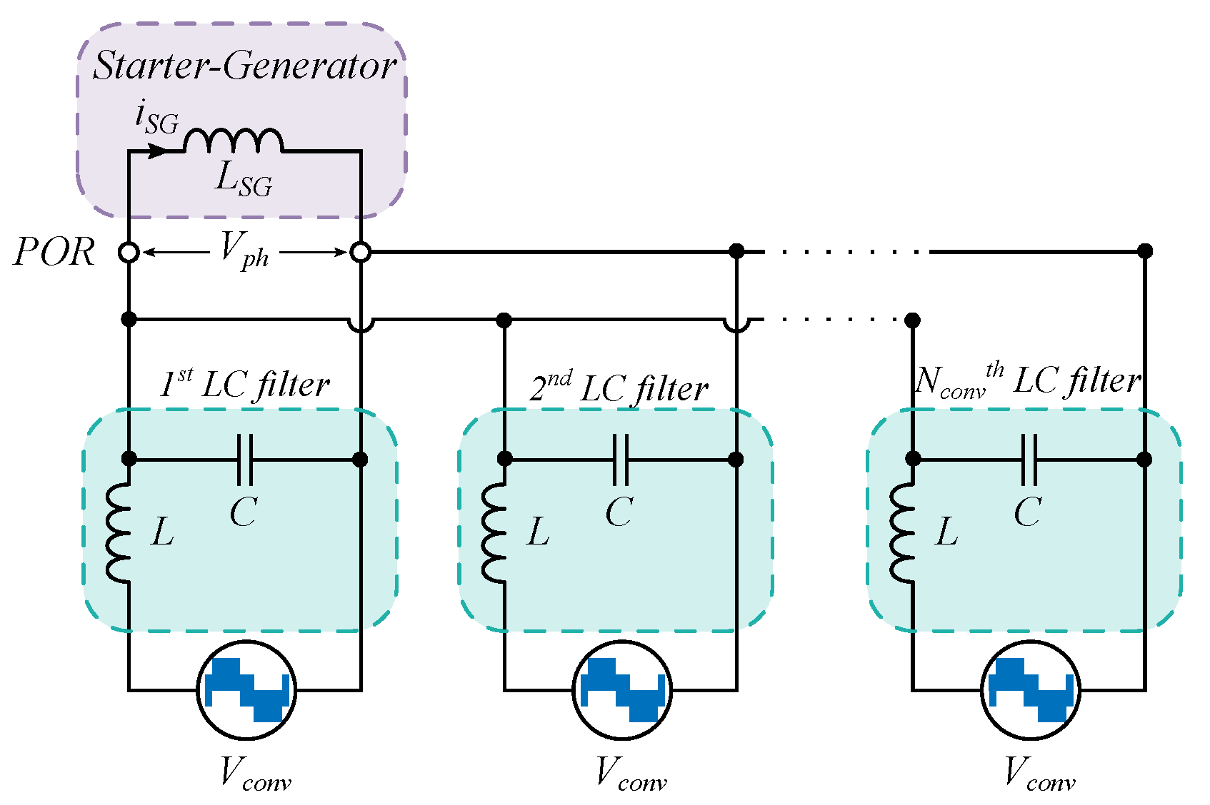
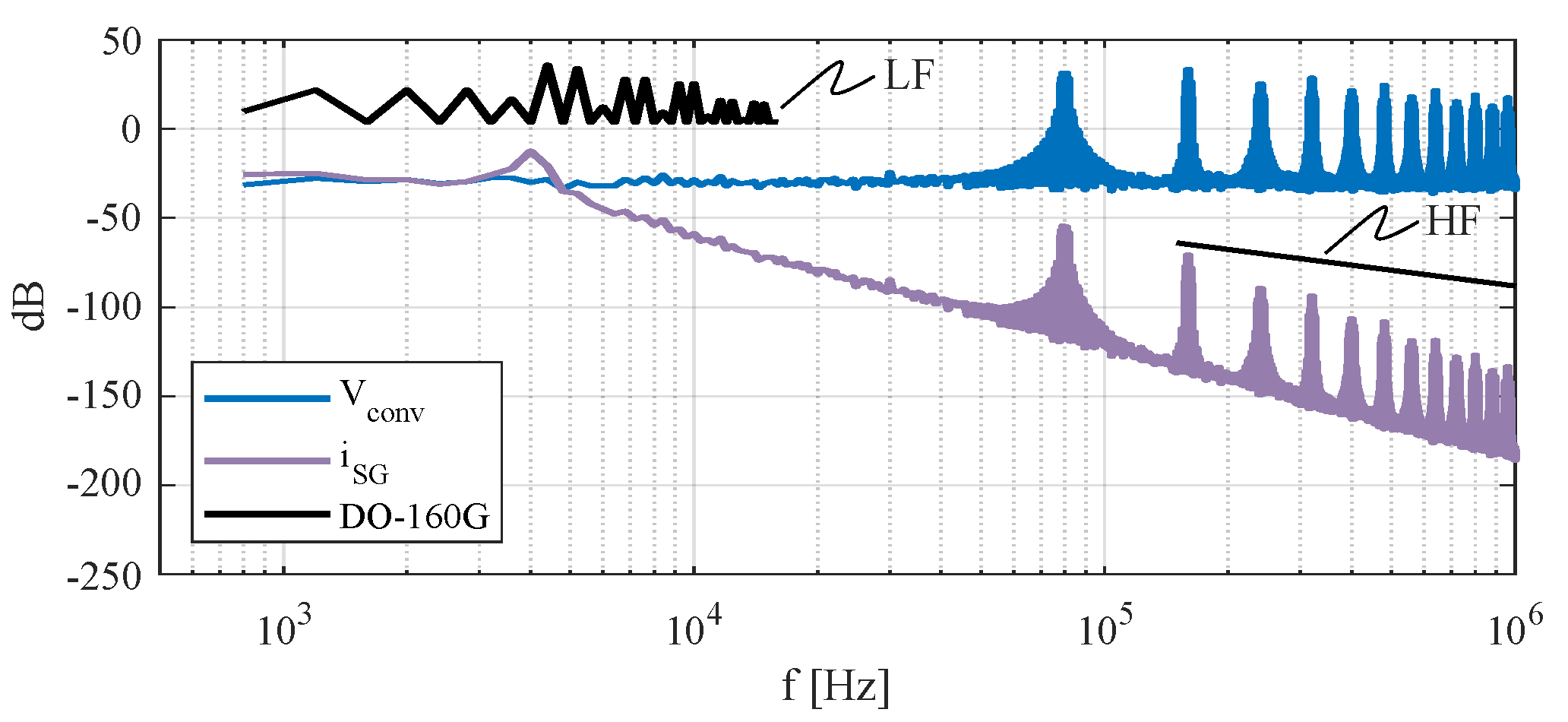
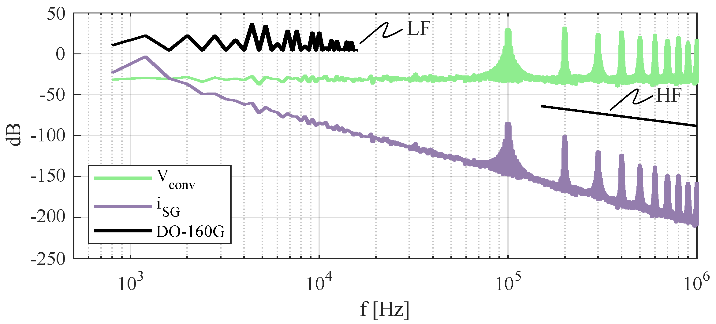
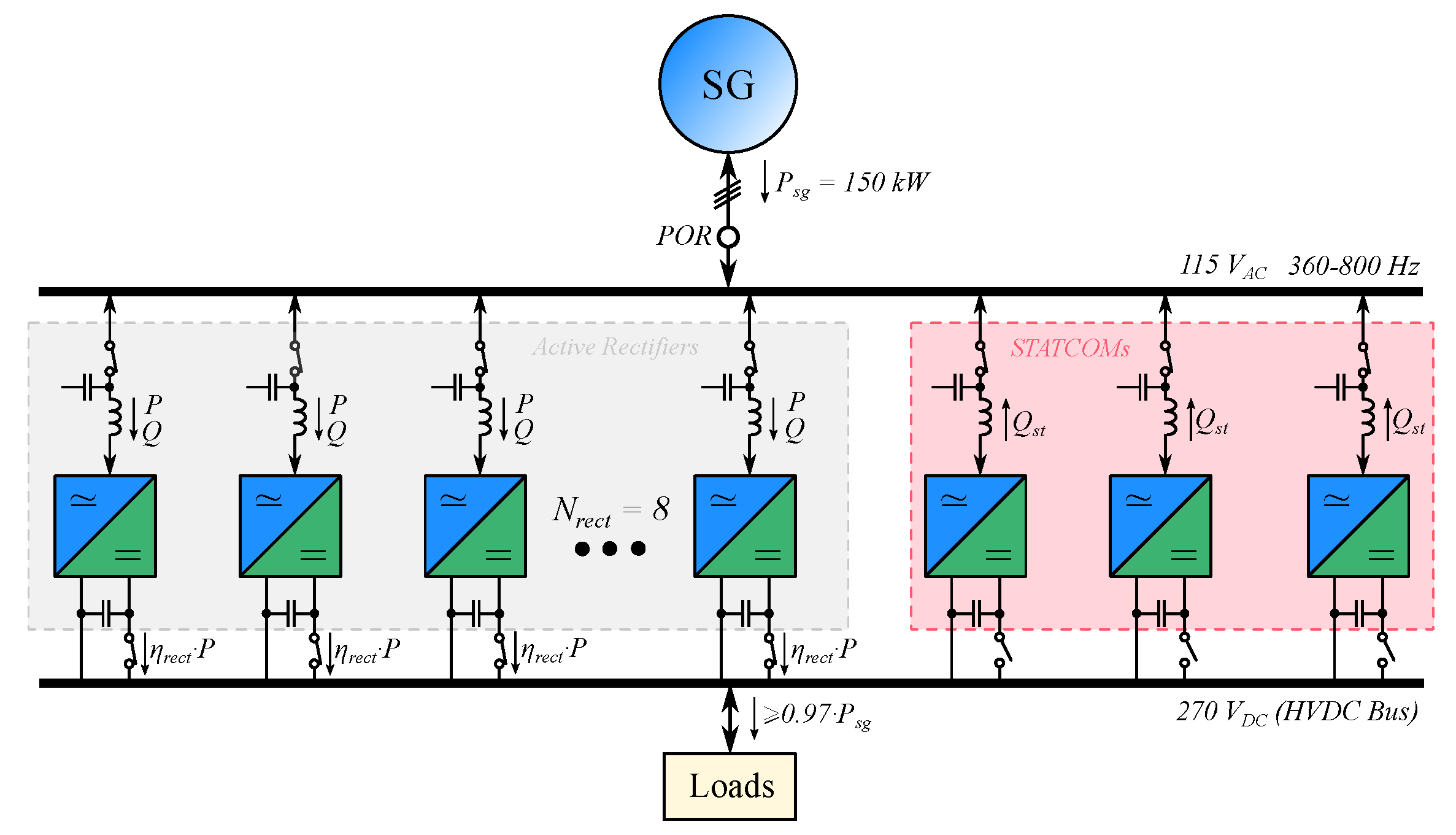
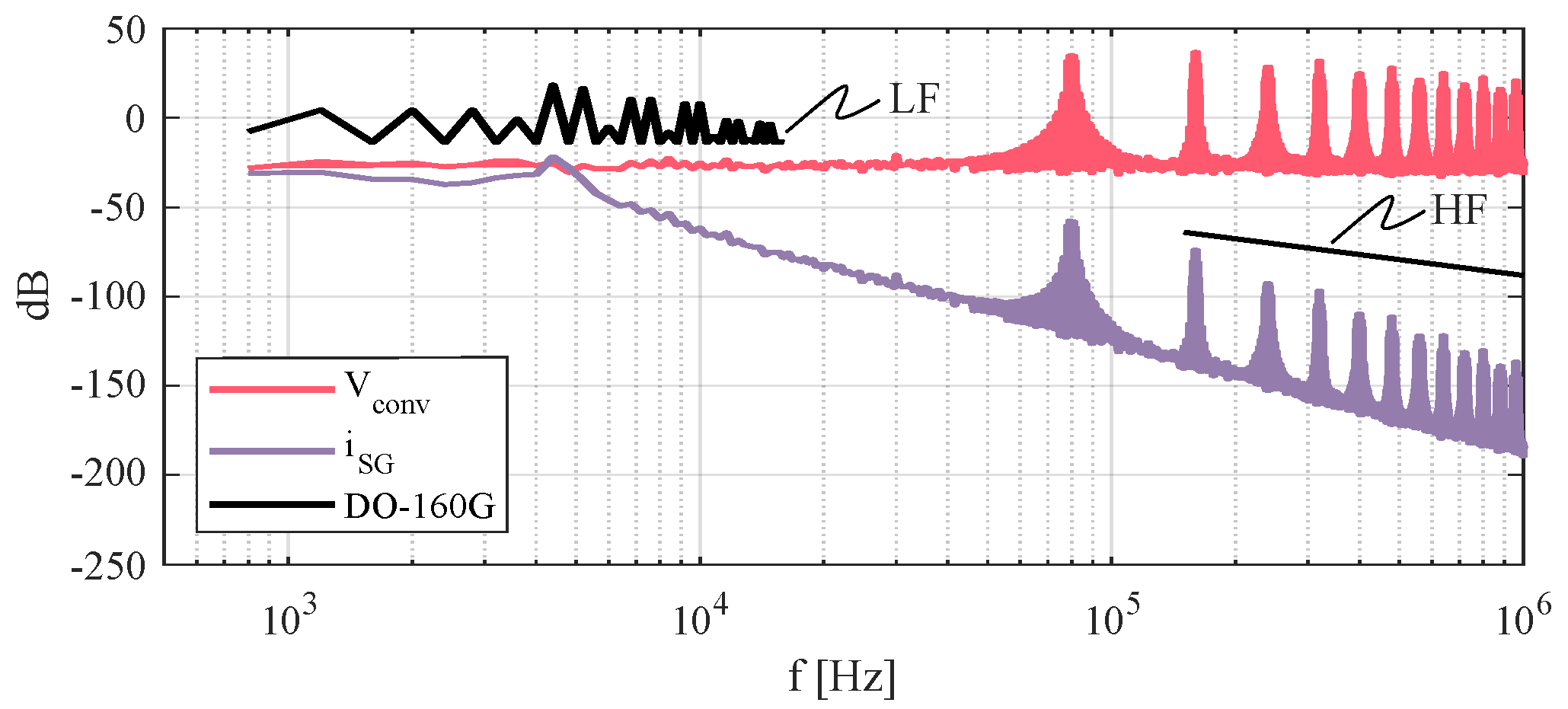
- Due to restrictive harmonic limitations imposed, a differential LCL filter mode was considered for this application [30,56], where the grid-side inductance corresponded to an assumed SG synchronous inductance of = 93.5 H (calculated in Appendix A) [57]. Thus, an LC filter was assumed for each power converter configuration. The power quality ( ≤ 3%) and harmonic requirements must be fulfilled at the point of regulation (POR), i.e., the point where the active modular architecture is connected to the SG. This concept is represented in Figure 7, where a considered number of synchronized converters, , are connected to the POR. Due to the converter parallelization, the filter inductance and capacitance for the ideal LCL filter of the overall architecture are defined as and , respectively. Thus, based on the transfer function of the equivalent single-phase LCL filter in [58], the transfer function of the architecture LCL filter is defined asSpecial attention should be paid to the third order filter term in (16), which presents a 60 dB/decade asymptote, since its cut-off frequency is determined by the term . Therefore, independent of the number of converters connected to the POR, the cut-off frequency of the 60 dB/decade asymptote is maintained constant. This fact provides the possibility of defining the input filter capacitor for high frequency harmonics filtering without considering .
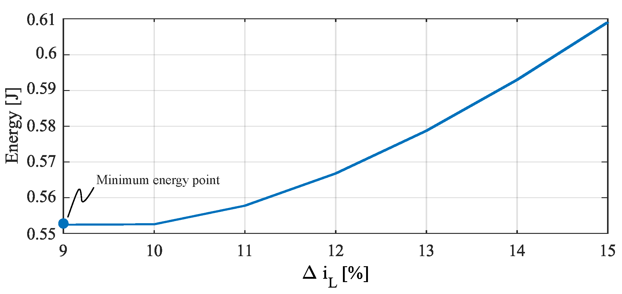
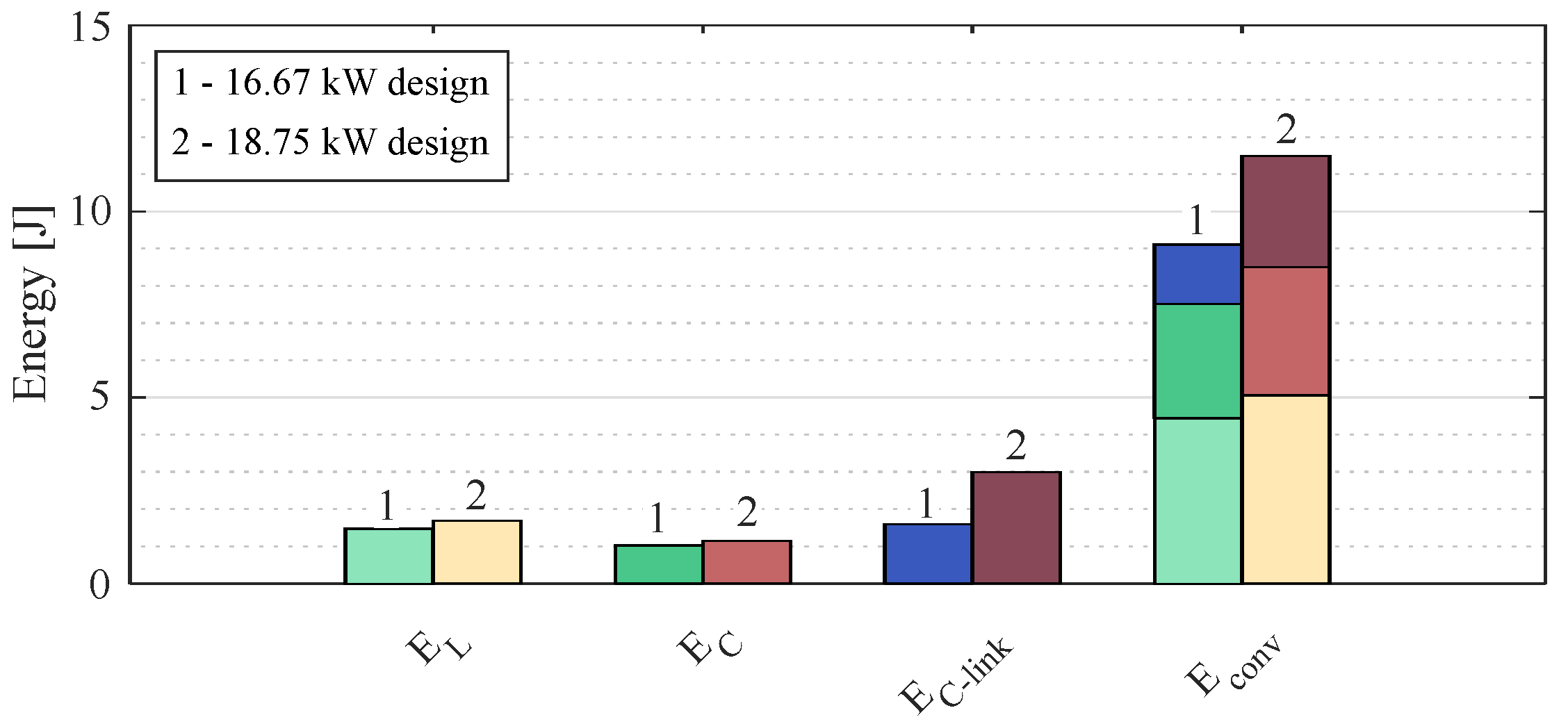
- The dc-link capacitor, , of the three configurations is defined for a specific peak-to-peak switching voltage ripple, , according to [59]. Hence,where represents the power converter switching frequency.
4.1. Two-Stage Architecture-2L
4.2. Single-Stage with Capacitor Bank Architecture-2L
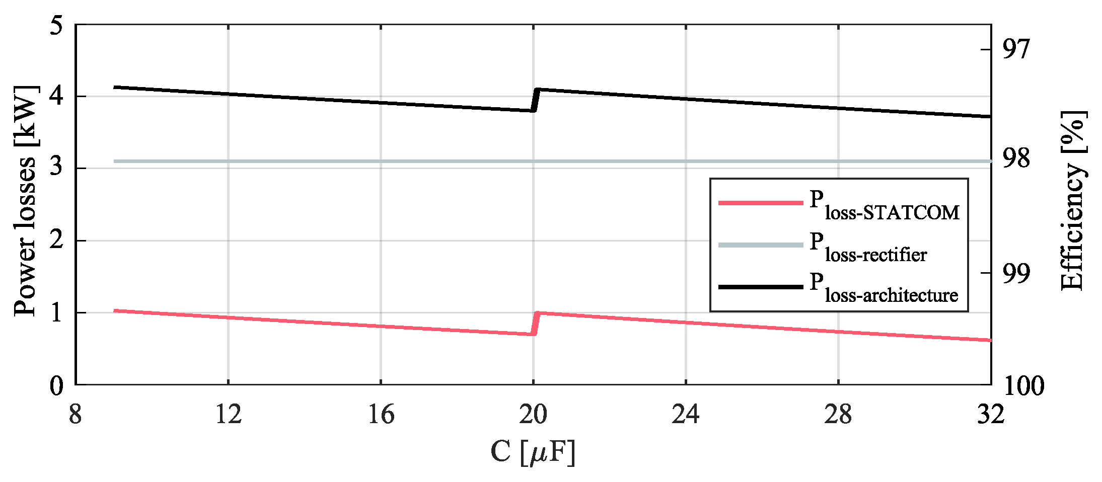
4.3. Single-Stage with STATCOM Architecture-2L
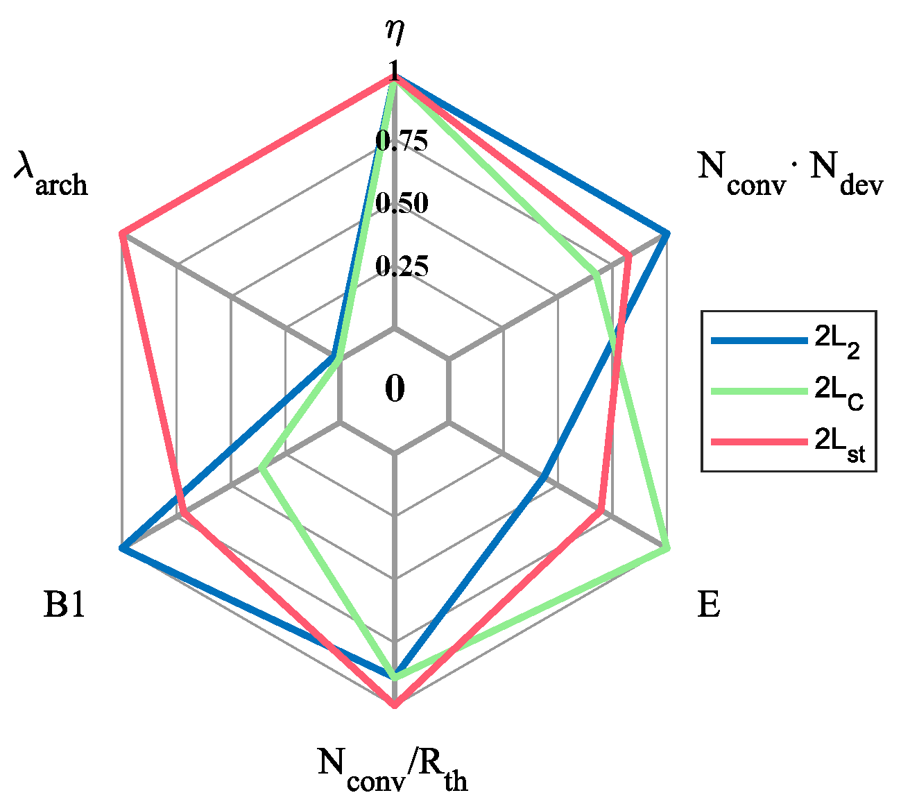
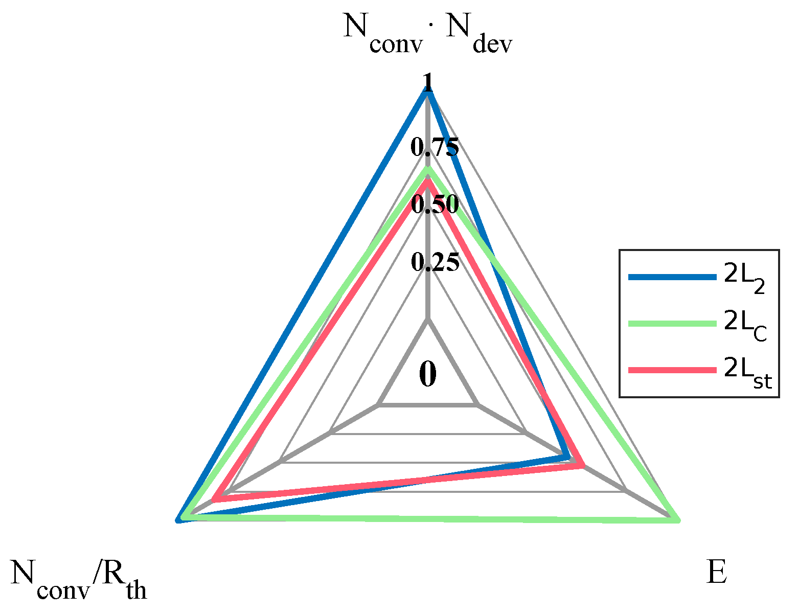
5. Comparative Analysis among Different Architectures
6. Conclusions
Author Contributions
Funding
Institutional Review Board Statement
Informed Consent Statement
Data Availability Statement
Acknowledgments
Conflicts of Interest
Appendix A. Starter-Generator Impedance Estimation
References
- Bozhko, S.; Hill, C.I.; Yang, T. More-Electric Aircraft: Systems and Modeling. In Wiley Encyclopedia of Electrical and Electronics Engineering; John Wiley & Sons, Inc.: Hoboken, NJ, USA, 2018; pp. 1–31. [Google Scholar]
- Ni, K.; Liu, Y.; Mei, Z.; Wu, T.; Hu, Y.; Wen, H.; Wang, Y. Electrical and Electronic Technologies in More-Electric Aircraft: A Review. IEEE Access 2019, 7, 76145–76166. [Google Scholar] [CrossRef]
- Sarlioglu, B.; Morris, C.T. More Electric Aircraft: Review, Challenges, and Opportunities for Commercial Transport Aircraft. IEEE Trans. Transp. Electrif. 2015, 1, 54–64. [Google Scholar] [CrossRef]
- Chen, J.; Wang, C.; Chen, J. Investigation on the Selection of Electric Power System Architecture for Future More Electric Aircraft. IEEE Trans. Transp. Electrif. 2018, 4, 563–576. [Google Scholar] [CrossRef]
- Liu, R.; Xu, L.; Kang, Y.; Hui, Y.; Li, Y. 230 VAC/28 VDC high-power density power supply for more electric aircraft applications. J. Eng. 2018, 2018, 499–505. [Google Scholar] [CrossRef]
- Buticchi, G.; Bozhko, S.; Liserre, M.; Wheeler, P.; Al-Haddad, K. On-Board Microgrids for the More Electric Aircraft—Technology Review. IEEE Trans. Ind. Electron. 2019, 66, 5588–5599. [Google Scholar] [CrossRef] [Green Version]
- Gong, G.; Heldwein, M.; Drofenik, U.; Minibock, J.; Mino, K.; Kolar, J. Comparative Evaluation of Three-Phase High-Power-Factor AC–DC Converter Concepts for Application in Future More Electric Aircraft. IEEE Trans. Ind. Electron. 2005, 52, 727–737. [Google Scholar] [CrossRef]
- Kolar, J.W.; Friedli, T. The Essence of Three-Phase PFC Rectifier Systems—Part I. IEEE Trans. Power Electron. 2013, 28, 176–198. [Google Scholar] [CrossRef]
- Trentin, A.; Sala, G.; Tarisciotti, L.; Galassini, A.; Degano, M.; Connor, P.; Golovanov, D.; Gerada, D.; Xu, Z.; La Rocca, A.; et al. Research and Realisation of High-Power Medium Voltage Active Rectifier Concepts for Future Hybrid-Electric Aircraft Generation. IEEE Trans. Ind. Electron. 2020, 0046, 1. [Google Scholar]
- Sahoo, S.; Zhao, X.; Kyprianidis, K. A Review of Concepts, Benefits, and Challenges for Future Electrical Propulsion-Based Aircraft. Aerospace 2020, 7, 44. [Google Scholar] [CrossRef] [Green Version]
- Dorn-Gomba, L.; Ramoul, J.; Reimers, J.; Emadi, A. Power Electronic Converters in Electric Aircraft: Current Status, Challenges, and Emerging Technologies. IEEE Trans. Transp. Electrif. 2020, 6, 1648–1664. [Google Scholar] [CrossRef]
- Bowman, C.L.; Marien, T.V.; Felder, J.L. Turbo- and Hybrid-Electrified Aircraft Propulsion for Commercial Transport. In Proceedings of the 2018 AIAA/IEEE Electric Aircraft Technologies Symposium; American Institute of Aeronautics and Astronautics: Reston, Virginia, 2018; pp. 1–8. [Google Scholar]
- Madonna, V.; Giangrande, P.; Galea, M. Electrical Power Generation in Aircraft: Review, Challenges, and Opportunities. IEEE Trans. Transp. Electrif. 2018, 4, 646–659. [Google Scholar] [CrossRef]
- Bozhko, S.; Yang, T.; Le Peuvedic, J.M.; Arumugam, P.; Degano, M.; La Rocca, A.; Xu, Z.; Rashed, M.; Fernando, W.; Hill, C.I.; et al. Development of Aircraft Electric Starter–Generator System Based on Active Rectification Technology. IEEE Trans. Transp. Electrif. 2018, 4, 985–996. [Google Scholar] [CrossRef]
- Garrido-Diez, D.; Baraia, I. Review of wide bandgap materials and their impact in new power devices. In Proceedings of the 2017 IEEE International Workshop of Electronics, Control, Measurement, Signals and their Application to Mechatronics (ECMSM), Donostia, Spain, 24–26 May 2017; pp. 1–6. [Google Scholar]
- Millan, J. A review of WBG power semiconductor devices. In Proceedings of the CAS 2012 International Semiconductor Conference, Sinaia, Romania, 15–17 October 2012; Volume 1, pp. 57–66. [Google Scholar]
- Reinhardt, K.; Marciniak, M. Wide-bandgap power electronics for the More Electric Aircraft. In Proceedings of the IECEC 96, 31st Intersociety Energy Conversion Engineering Conference, Washington, DC, USA, 11–16 August 1996; Volume 1, pp. 127–132. [Google Scholar]
- Brewer, R.A. High temperature electronics for demanding aircraft applications. In Proceedings of the 2018 International Applied Computational Electromagnetics Society Symposium (ACES), Beijing China, 29 July–1 August 2018; pp. 1–2. [Google Scholar]
- Perdikakis, W.; Scott, M.J.; Yost, K.J.; Kitzmiller, C.; Hall, B.; Sheets, K.A. Comparison of Si and SiC EMI and Efficiency in a Two-Level Aerospace Motor Drive Application. IEEE Trans. Transp. Electrif. 2020, 6, 1401–1411. [Google Scholar] [CrossRef]
- Kharanaq, F.A.; Emadi, A.; Bilgin, B. Modeling of Conducted Emissions for EMI Analysis of Power Converters: State-of-the-Art Review. IEEE Access 2020, 8, 189313–189325. [Google Scholar] [CrossRef]
- Zhang, H.; Ge, B.; Liu, Y.; Bayhan, S.; Balog, R.S.; Abu-Rub, H. Comparison of GaN and SiC power devices in application to MW-scale quasi-Z-source cascaded multilevel inverters. In Proceedings of the 2016 IEEE Energy Conversion Congress and Exposition (ECCE), Milwaukee, MI, USA, 18–22 September 2016; pp. 1–7. [Google Scholar]
- Valente, G.; Sumsurooah, S.; Hill, C.I.; Rashed, M.; Vakil, G.; Bozhko, S.; Gerada, C. Design Methodology and Parametric Design Study of the On-Board Electrical Power System for Hybrid Electric Aircraft Propulsion. In Proceedings of the 10th International Conference on Power Electronics, Machines and Drives (PEMD 2020). Institution of Engineering and Technology, Online, 15–17 December 2021; pp. 448–454. Available online: https://ieeexplore.ieee.org/document/9545239 (accessed on 1 February 2022).
- Lim, Z.; Liu, Y.; Zhang, L.; Pou, J.; Simanjorang, R.; Gupta, A. Design of 100 kVA SiC Power Converter for Aircraft Electric Starter Generator. In Proceedings of the 2018 IEEE 4th Southern Power Electronics Conference (SPEC), Singapore, 10–13 December 2018; pp. 1–9. [Google Scholar]
- Hartmann, M. Ultra-Compact and Ultra-Efficient Three-Phase PWM Rectifier Systems for More Electric Aircraft. Ph.D. Dissertation, ETH Zurich, Zurich, Switzerland, 2011. [Google Scholar]
- Borovic, U.; Zhao, S.; Silva, M.; Bouvier, Y.E.; Vasic, M.; Oliver, J.A.; Alou, P.; Cobos, J.A.; Arevalo, F.; Garcia-Tembleque, J.; et al. Comparison of three-phase active rectifier solutions for avionic applications: Impact of the avionic standard DO-160 F and failure modes. In Proceedings of the 2016 IEEE Energy Conversion Congress and Exposition (ECCE), Milwaukee, MI, USA, 18–22 September 2016; pp. 1–8. [Google Scholar]
- Singh, A.; Mallik, A.; Khaligh, A. A Comprehensive Design and Optimization of the DM EMI Filter in a Boost PFC Converter. IEEE Trans. Ind. Appl. 2018, 54, 2023–2031. [Google Scholar] [CrossRef]
- Mallik, A.; Ding, W.; Khaligh, A. A Comprehensive Design Approach to an EMI Filter for a 6-kW Three-Phase Boost Power Factor Correction Rectifier in Avionics Vehicular Systems. IEEE Trans. Veh. Technol. 2017, 66, 2942–2951. [Google Scholar] [CrossRef]
- Atutxa, U.; Baraia-Etxaburu, I.; Lopez, V.M.; Rujas, A. Suitability and Performance Evaluation of Active Rectifier Topologies for More Electric Aircraft. In Proceedings of the 2021 IEEE Vehicle Power and Propulsion Conference (VPPC), Gijón, Spain, 25–28 October 2021. [Google Scholar]
- Brombach, J.; Lucken, A.; Nya, B.; Johannsen, M.; Schulz, D. Comparison of different electrical HVDC-architectures for aircraft application. In Proceedings of the 2012 Electrical Systems for Aircraft, Railway and Ship Propulsion, Bologna, Italy, 16–18 October 2012; pp. 1–6. [Google Scholar]
- RTCA. DO-160G: Environmental Conditions and Test Procedures for Airborne Equipment; Technical Report; RTCA: New York, NY, USA, 2011. [Google Scholar]
- Aerospace Technology Institute. INSIGHT-07 Electrical Power Systems; Aerospace Technology Institute: London, UK, 2018; pp. 1–16. [Google Scholar]
- Malinowski, M. AC-Line Sensorless Control Strategies for Three-Phase PWM Rectifiers. Ph.D. Thesis, Warsaw University of Technology, Warsaw, Poland, 2001. [Google Scholar]
- Sanchez-Ruiz, A.; Mazuela, M.; Alvarez, S.; Abad, G.; Baraia, I. Medium Voltage–High Power Converter Topologies Comparison Procedure, for a 6.6 kV Drive Application Using 4.5 kV IGBT Modules. IEEE Trans. Ind. Electron. 2012, 59, 1462–1476. [Google Scholar] [CrossRef]
- Borovic, U.; Zhao, S.; Silva, M.; Bouvier, Y.; Vasic, M.; Ramírez, J.A.O.; Cervera, P.A.; Márquez, J.A.C.; Pejovic, P. Comparison of Three-Phase Active Rectifiers For Aircraft Application. In Proceedings of the Seminario Anual de Automática, Electrónica Industrial e Instrumentación SAAEI 2015, Córdoba, Spain, 3–5 July 2015; pp. 1–7. [Google Scholar]
- Kouro, S.; Malinowski, M.; Gopakumar, K.; Pou, J.; Franquelo, L.G.; Bin, W.; Rodriguez, J.; Pérez, M.A.; Leon, J.I. Recent Advances and Industrial Applications of Multilevel Converters. IEEE Trans. Ind. Electron. 2010, 57, 2553–2580. [Google Scholar] [CrossRef]
- Dermouche, R.; Talaoubrid, A.; Barazane, L.; Sellami, Y.; Tadjine, M.; Zioui, N. Qualitative and quantitative analysis of the reliability of NPC and ANPC power converters for aeronautical applications. Alex. Eng. J. 2021. [Google Scholar] [CrossRef]
- Gong, G.; Drofenik, U.; Kolar, J. 12-pulse rectifier for more electric aircraft applications. In Proceedings of the IEEE International Conference on Industrial Technology, Maribor, Slovenia, 10–12 December 2003; Volume 2, pp. 1096–1101. [Google Scholar]
- Gonzalez-Hernando, F.; San-Sebastian, J.; Arias, M.; Rujas, A.; Mir, L. Active Thermal Control for Lifetime Extension of Traction Converter. In Proceedings of the 10th International Conference on Power Electronics, Machines and Drives (PEMD 2020), Online, 15–17 December 2021; pp. 1007–1012. [Google Scholar]
- Guacci, M.; Bortis, D.; Kolar, J.W. High-Efficiency Weight-Optimized Fault-Tolerant Modular Multi-Cell Three-Phase GaN Inverter for Next Generation Aerospace Applications. In Proceedings of the 2018 IEEE Energy Conversion Congress and Exposition (ECCE), Portland, OR, USA, 23–27 September 2018; pp. 1334–1341. [Google Scholar]
- Harikumaran, J.; Buticchi, G.; Migliazza, G.; Madonna, V.; Giangrande, P.; Costabeber, A.; Wheeler, P.; Galea, M. Failure Modes and Reliability Oriented System Design for Aerospace Power Electronic Converters. IEEE Open J. Ind. Electron. Soc. 2021, 2, 53–64. [Google Scholar] [CrossRef]
- Heldwein, M.L. EMC Filtering of Three-Phase PWM Converters. Ph.D Thesis, ETH Zurich, Zurich, Switzerland, 2008. [Google Scholar]
- Seshasayee, N. Understanding Thermal Dissipation and Design of a Heatsink; Technical Report; Texas Instruments: Dallas, TX, USA, 2011. [Google Scholar]
- IQ-Evolution Gmbh. 3D Printed Micro Cooler for Power Electronics; IQ-Evolution Gmbh: Aachen, Germany, 2020. [Google Scholar]
- Shen, Y.; Chub, A.; Wang, H.; Vinnikov, D.; Liivik, E.; Blaabjerg, F. Wear-Out Failure Analysis of an Impedance-Source PV Microinverter Based on System-Level Electrothermal Modeling. IEEE Trans. Ind. Electron. 2019, 66, 3914–3927. [Google Scholar] [CrossRef] [Green Version]
- Huber, J.E.; Kolar, J.W. Optimum Number of Cascaded Cells for High-Power Medium-Voltage AC–DC Converters. IEEE J. Emerg. Sel. Top. Power Electron. 2017, 5, 213–232. [Google Scholar] [CrossRef]
- Testa, A.; De Caro, S.; Russo, S. A Reliability Model for Power MOSFETs Working in Avalanche Mode Based on an Experimental Temperature Distribution Analysis. IEEE Trans. Power Electron. 2012, 27, 3093–3100. [Google Scholar] [CrossRef]
- Lichtenwalner, D.J.; Hull, B.; Van Brunt, E.; Sabri, S.; Gajewski, D.A.; Grider, D.; Allen, S.; Palmour, J.W.; Akturk, A.; McGarrity, J. Reliability studies of SiC vertical power MOSFETs. In Proceedings of the 2018 IEEE International Reliability Physics Symposium (IRPS), Burlingame, CA, USA, 11–15 March 2018; Volume 2018-March, pp. 2B.2–1–2B.2–6. [Google Scholar]
- Lichtenwalner, D.J.; Akturk, A.; McGarrity, J.; Richmond, J.; Barbieri, T.; Hull, B.; Grider, D.; Allen, S.; Palmour, J.W. Reliability of SiC Power Devices against Cosmic Ray Neutron Single-Event Burnout. Mater. Sci. Forum 2018, 924, 559–562. [Google Scholar] [CrossRef]
- Akturk, A.; McGarrity, J.M.; Goldsman, N.; Lichtenwalner, D.J.; Hull, B.; Grider, D.; Wilkins, R. Predicting Cosmic Ray-Induced Failures in Silicon Carbide Power Devices. IEEE Trans. Nucl. Sci. 2019, 66, 1828–1832. [Google Scholar] [CrossRef]
- Felgemacher, C.; Araujo, S.V.; Zacharias, P.; Nesemann, K.; Gruber, A. Cosmic radiation ruggedness of Si and SiC power semiconductors. In Proceedings of the 2016 28th International Symposium on Power Semiconductor Devices and ICs (ISPSD), Žofín Palace, Prague, Czech Republic, 12–16 June 2016; Volume 2016-July, pp. 51–54. [Google Scholar]
- ABB. Failure Rates of IGBT Modules Due to Cosmic Rays; Technical Report; ABB: Zürich, Switzerland, 2019. [Google Scholar]
- Wintrich, A.; Nicolai, U.; Tursky, W.; Reimann, T. Application Manual Power Semiconductors, 2nd ed.; ISLE Verlag: Berlin, Germany, 2015; p. 466. [Google Scholar]
- Barbagallo, C.; Rizzo, S.A.; Scelba, G.; Scarcella, G.; Cacciato, M. On the Lifetime Estimation of SiC Power MOSFETs for Motor Drive Applications. Electronics 2021, 10, 324. [Google Scholar] [CrossRef]
- Qiu, Z.; Zhang, J.; Ning, P.; Wen, X. Reliability modeling and analysis of SiC MOSFET power modules. In Proceedings of the IECON 2017-43rd Annual Conference of the IEEE Industrial Electronics Society, Beijing, China, 29 October 2017; pp. 1459–1463. [Google Scholar]
- Anoldo, L.; Triolo, C.; Panarello, S.; Garesci, F.; Russo, S.; Messina, A.A.; Calabretta, M.; Patane, S. Study of the Thermomechanical Strain Induced by Current Pulses in SiC-Based Power MOSFET. IEEE Electron. Device Lett. 2021, 42, 1089–1092. [Google Scholar] [CrossRef]
- Han, Y.; Yang, M.; Li, H.; Yang, P.; Xu, L.; Coelho, E.A.A.; Guerrero, J.M. Modeling and Stability Analysis of LCL -Type Grid-Connected Inverters: A Comprehensive Overview. IEEE Access 2019, 7, 114975–115001. [Google Scholar] [CrossRef]
- Pyrhönen, J.; Jokinen, T.; Hrabovcová, V. Design of Rotating Electrical Machines; John Wiley and Sons Ltd.: Chichester, UK, 2013; p. 614. [Google Scholar]
- Ruan, X.; Wang, X.; Pan, D.; Yang, D.; Li, W.; Bao, C. Control Techniques for LCL-Type Grid-Connected Inverters, 1st ed.; CPSS Power Electronics Series; Springer: Singapore, 2018; pp. XXII, 305. [Google Scholar]
- Vujacic, M.; Hammami, M.; Srndovic, M.; Grandi, G. Analysis of dc-Link Voltage Switching Ripple in Three-Phase PWM Inverters. Energies 2018, 11, 471. [Google Scholar] [CrossRef] [Green Version]
- Ejury, J. Buck Converter Design; Technical Report; Mouser: Mansfield, TX, USA, 2013. [Google Scholar]
- Reznik, A.; Simoes, M.G.; Al-Durra, A.; Muyeen, S.M. LCL Filter Design and Performance Analysis for Grid-Interconnected Systems. IEEE Trans. Ind. Appl. 2014, 50, 1225–1232. [Google Scholar] [CrossRef]


| Parameter | Value |
|---|---|
| Nominal phase RMS voltage, | 115 V |
| Steady state phase RMS voltage | 100–122 V |
| Steady state frequency, f | 360–800 Hz |
| Power factor, PF | 0.85–1 |
| Current total harmonic distortion, THD | ≤3% |
| Nominal DC voltage, | 270 V |
| Steady state DC voltage | 250–280 V |
| Architecture power rating | 150 kW |
| Targeted efficiency | ≥97% |
| Configuration | ||
|---|---|---|
| 2L & 2L | 270 V | 1.74 · 10 |
| 2L | 312 V | 3.38 · 10 |
| 2L | 459 V | 0.0304 |
| 2L | 2L | 2L | |
|---|---|---|---|
| Converter nominal power, P | 18.75 kW | 16.67 kW | 18.75 kW |
| N° of SiC MOSFET, | 10 | 6 | 6 |
| N° of converters, | 8 | 9 | 8 + 3 |
| AC/DC switching frequency, | 80 kHz | 100 kHz | 80 kHz |
| SG current distortion, | 0.05% | 0.11% | 0.13% |
| SG inductance, | 93.5 H | 93.5 H | 93.5 H |
| Input filter inductance, L | 94 H | 342.25 H | 191.4 H |
| Input filter capacitance, C | 18 F | 68.64 F | 19 F |
| DC bus capacitance, | 44.73 F | 42.82 F | 52.18 F |
| AC/DC stage output voltage, | 312 V | 270 V | 270 V & 459 V |
| DC/DC stage output voltage, | 270 V | - | - |
| DC/DC switching frequency, | 75 kHz | - | - |
| DC/DC inductance, | 139.6 H | - | - |
| DC/DC capacitance, | 1.07 F | - | - |
| Maximum temperature rise, | 55.13 °C | 66.28 °C | 58.73 °C |
| Heat sink thermal resistance, | 0.027 °C/W | 0.03 °C/W | 0.032 °C/W |
Publisher’s Note: MDPI stays neutral with regard to jurisdictional claims in published maps and institutional affiliations. |
© 2022 by the authors. Licensee MDPI, Basel, Switzerland. This article is an open access article distributed under the terms and conditions of the Creative Commons Attribution (CC BY) license (https://creativecommons.org/licenses/by/4.0/).
Share and Cite
Atutxa, U.; Baraia-Etxaburu, I.; López, V.M.; González-Hernando, F.; Rujas, A. Multi-Objective Comparative Analysis of Active Modular Rectifier Architectures for a More Electric Aircraft. Aerospace 2022, 9, 98. https://doi.org/10.3390/aerospace9020098
Atutxa U, Baraia-Etxaburu I, López VM, González-Hernando F, Rujas A. Multi-Objective Comparative Analysis of Active Modular Rectifier Architectures for a More Electric Aircraft. Aerospace. 2022; 9(2):98. https://doi.org/10.3390/aerospace9020098
Chicago/Turabian StyleAtutxa, Unai, Igor Baraia-Etxaburu, Víctor Manuel López, Fernando González-Hernando, and Alejandro Rujas. 2022. "Multi-Objective Comparative Analysis of Active Modular Rectifier Architectures for a More Electric Aircraft" Aerospace 9, no. 2: 98. https://doi.org/10.3390/aerospace9020098