Defect Detection in Printed Circuit Boards Using You-Only-Look-Once Convolutional Neural Networks


 and
and
Abstract
:1. Introduction
2. Materials and Methods
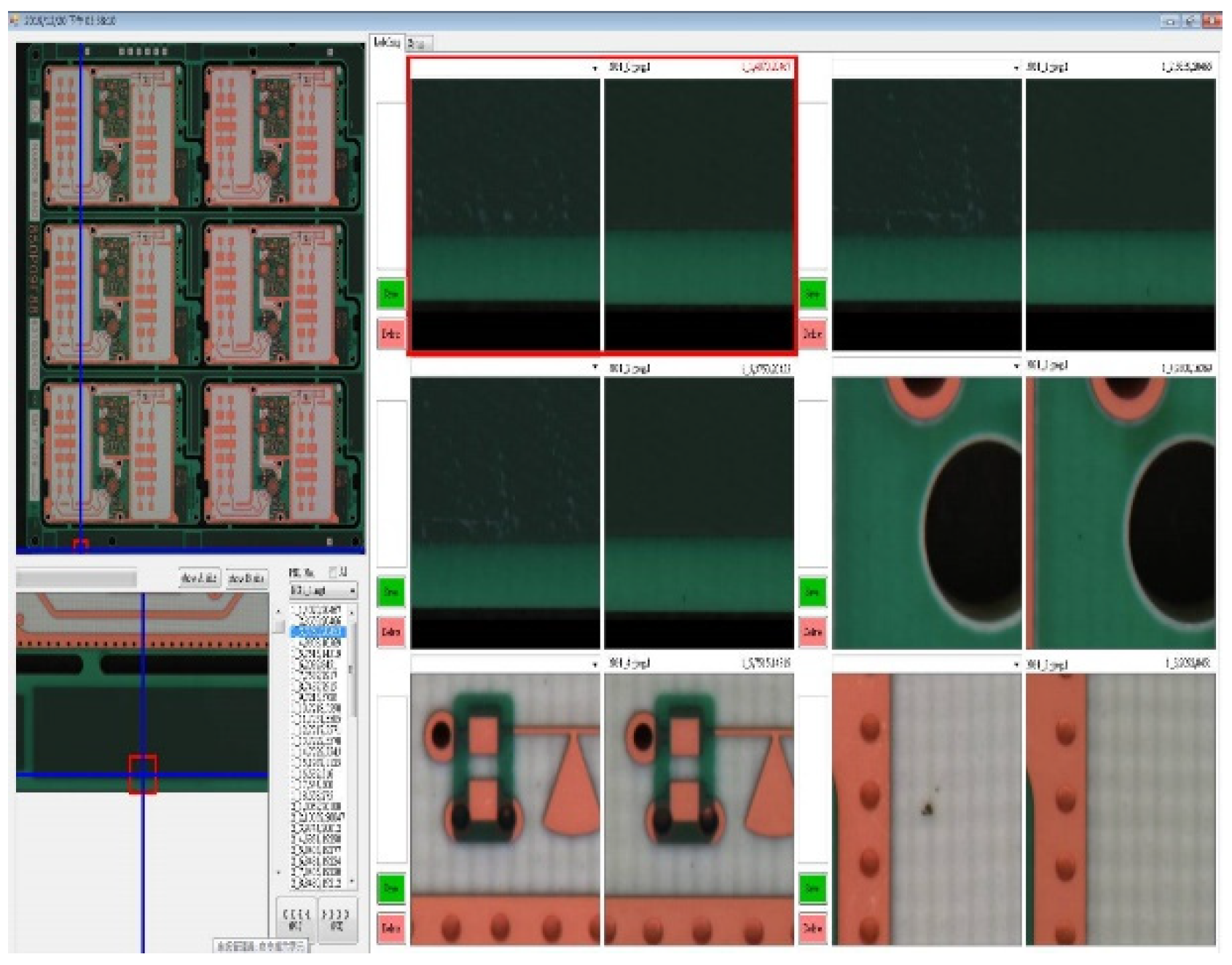
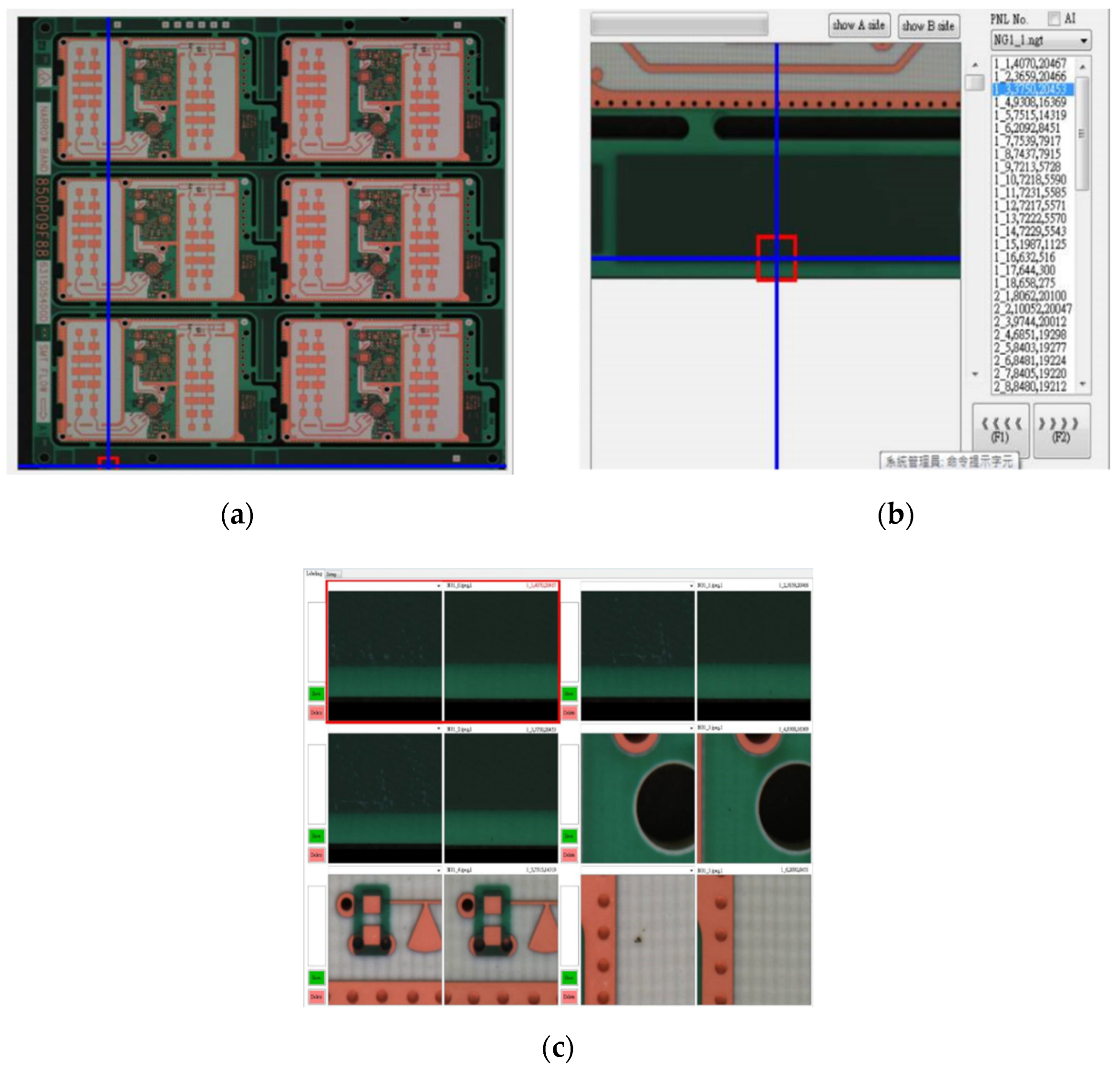
2.1. PCB Data Set
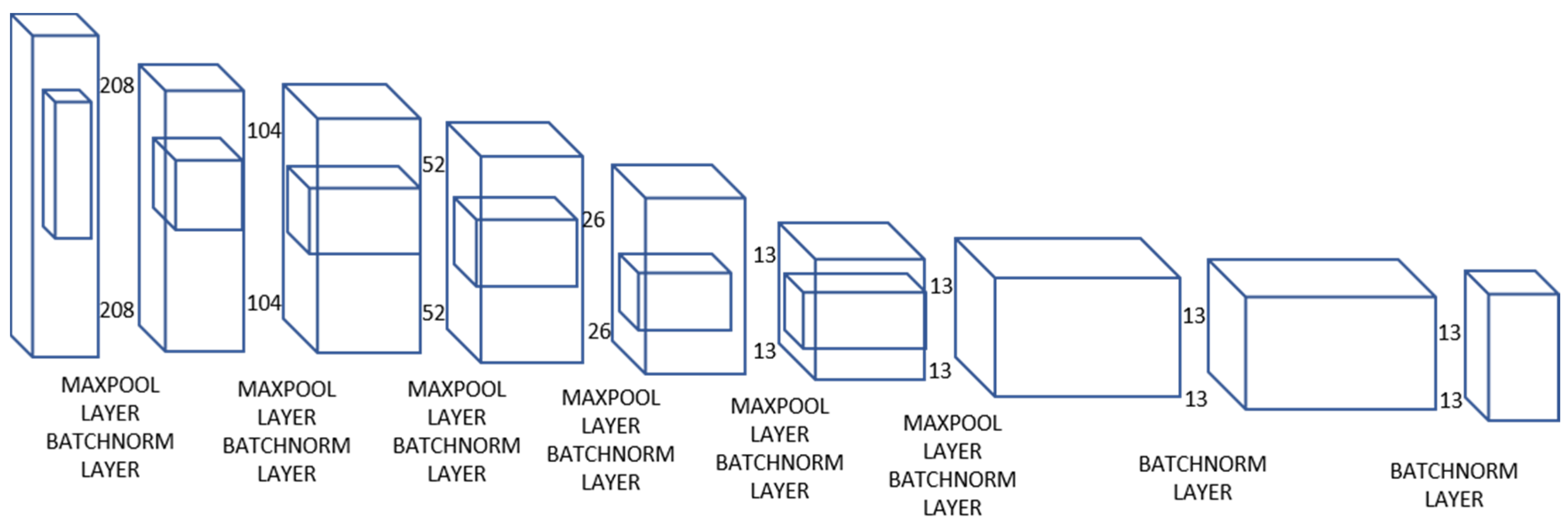
2.2. Architecture of Tiny-YOLO-v2
2.3. Convolutional Layer
2.4. Activation Function
2.5. Pooling Layer
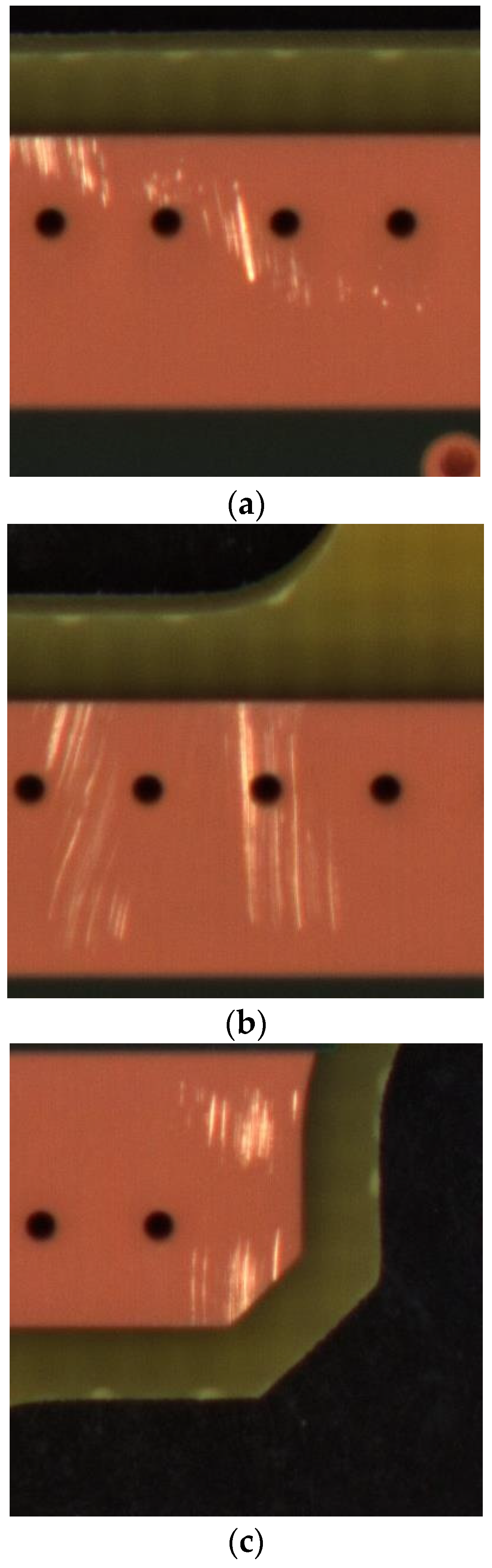
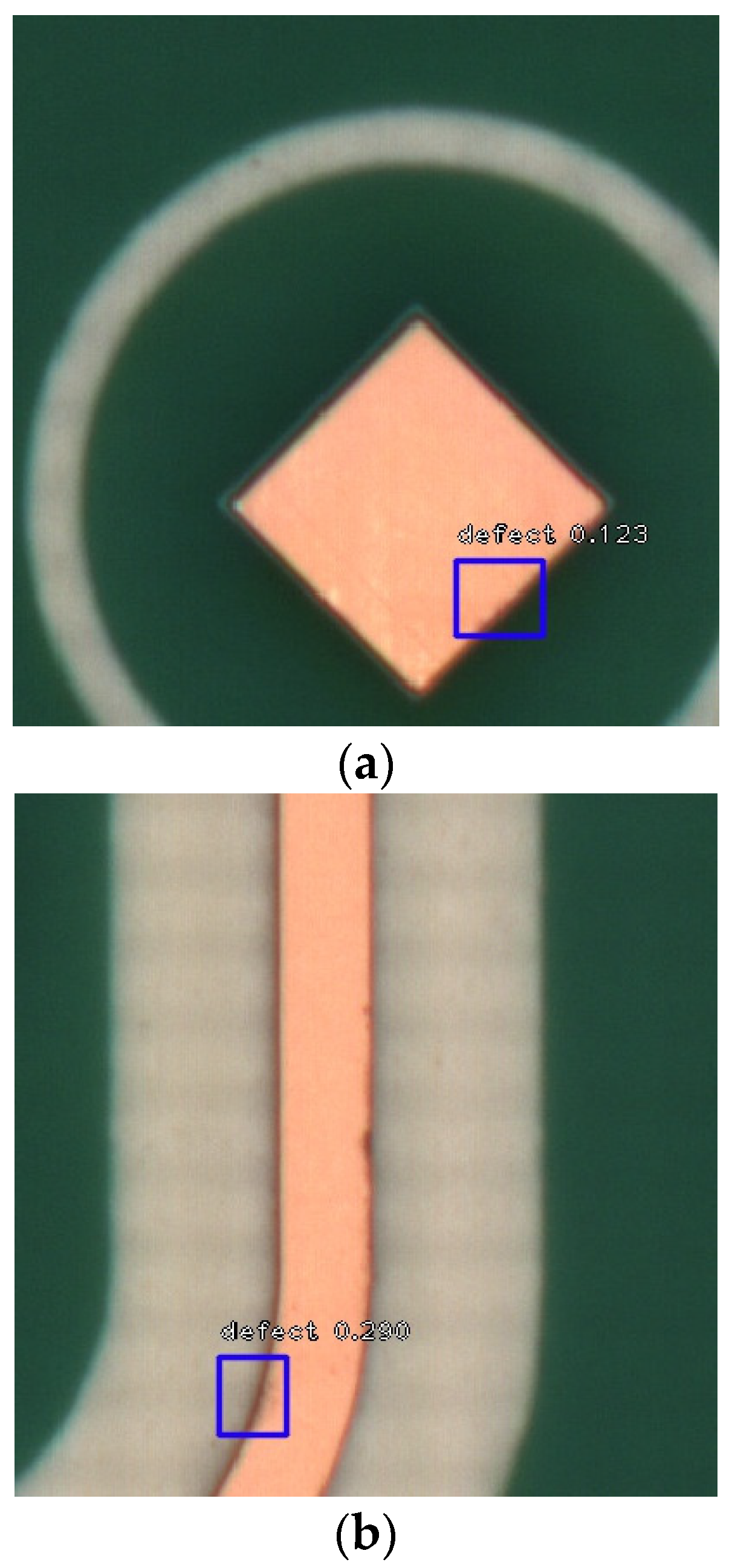
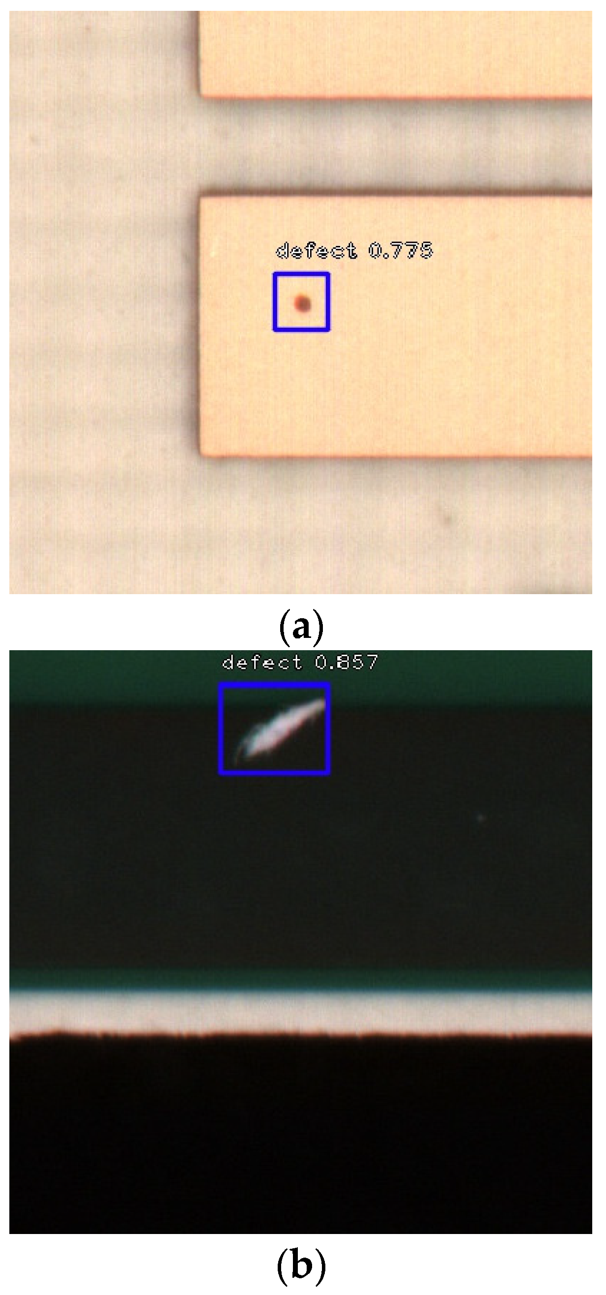
3. Results
4. Discussion
5. Conclusions
Author Contributions
Funding
Conflicts of Interest
References
- Suzuki, H.; Junkosha Co Ltd. Official Gazette of the United States Patent and Trademark. Printed Circuit Board. U.S. Patent US 4,640,866, 16 March 1987. [Google Scholar]
- Matsubara, H.; Itai, M.; Kimura, K.; NGK Spark Plug Co Ltd. Patents assigned to NGK spark plug. Printed Circuit Board. U.S. Patent US 6,573,458, 12 September 2003. [Google Scholar]
- Magera, J.A.; Dunn, G.J.; Motorola Solutions Inc. The Printed Circuit Designer’s Guide to Flex and Rigid-Flex Fundamentals. Printed Circuit Board. U.S. Patent US 7,459,202, 21 August 2008. [Google Scholar]
- Cho, H.S.; Yoo, J.G.; Kim, J.S.; Kim, S.H.; Samsung Electro Mechanics Co Ltd. Official Gazette of the United States Patent and Trademark. Printed Circuit Board. U.S. Patent US 8,159,824, 16 March 2012. [Google Scholar]
- Chauhan, A.P.S.; Bhardwaj, S.C. Detection of bare PCB defects by image subtraction method using machine vision. In Proceedings of the World Congress on Engineering, London, UK, 6–8 July 2011; Volume 2, pp. 6–8. [Google Scholar]
- Khalid, N.K.; Ibrahim, Z. An Image Processing Approach towards Classification of Defects on Printed Circuit Board. Ph.D. Thesis, University Technology Malaysia, Johor, Malaysia, 2007. [Google Scholar]
- Bengio, Y.; Courville, A.; Vincent, P. Representation Learning: A Review and New Perspectives. IEEE Trans. Pattern Anal. Mach. Intell. 2013, 35, 1798–1828. [Google Scholar] [CrossRef] [PubMed]
- Malge, P.S. PCB Defect Detection, Classification and Localization using Mathematical Morphology and Image Processing Tools. Int. J. Comput. Appl. 2014, 87, 40–45. [Google Scholar]
- Takada, Y.; Shiina, T.; Usami, H.; Iwahori, Y. Defect Detection and Classification of Electronic Circuit Boards Using Keypoint Extraction and CNN Features. In Proceedings of the Ninth International Conferences on Pervasive Patterns and Applications Defect, Athens, Greece, 19–23 February 2017; pp. 113–116. [Google Scholar]
- Anitha, D.B.; Mahesh, R. A Survey on Defect Detection in Bare PCB and Assembled PCB using Image Processing Techniques. In Proceedings of the 2017 International Conference on Wireless Communications, Signal Processing and Networking (WiSPNET), Chennai, India, 22–24 March 2017; pp. 39–43. [Google Scholar]
- Crispin, A.J.; Rankov, V. Automated inspection of PCB components using a genetic algorithm template-matching approach. Int. J. Adv. Manuf. Technol. 2007, 35, 293–300. [Google Scholar] [CrossRef] [Green Version]
- Raihan, F.; Ce, W. PCB Defect Detection USING OPENCV with Image Subtraction Method. In Proceedings of the 2017 International Conference on Information Management and Technology (ICIMTech), Singapore, 27–29 December 2017; pp. 204–209. [Google Scholar]
- Hosseini, H.; Xiao, B.; Jaiswal, M.; Poovendran, R. On the Limitation of Convolutional Neural Networks in Recognizing Negative Images. In Proceedings of the 2017 16th IEEE International Conference on Machine Learning and Applications (ICMLA), Cancun, Mexico, 18–21 December 2017; pp. 352–358. [Google Scholar]
- Tao, X.; Wang, Z.; Zhang, Z.; Zhang, D.; Xu, D.; Gong, X.; Zhang, L. Wire Defect Recognition of Spring-Wire Socket Using Multitask Convolutional Neural Networks. IEEE Trans. Compon. Packag. Manuf. Technol. 2018, 8, 689–698. [Google Scholar] [CrossRef]
- Uijlings, J.R.R.; Van De Sande, K.E.A.; Gevers, T.; Smeulders, A.W.M. Selective Search for Object Recognition. Int. J. Comput. Vis. 2012, 104, 154–171. [Google Scholar] [CrossRef] [Green Version]
- Girshick, R.; Donahue, J.; Darrell, T.; Malik, J. Rich feature hierarchies for accurate object detection and semantic segmentation. In Proceedings of the 2014 IEEE Conference on Computer Vision and Pattern Recognition, Columbus, OH, USA, 23–28 June 2014; pp. 580–587. [Google Scholar]
- He, K.; Zhang, X.; Ren, S.; Sun, J. Deep residual learning for image recognition. arXiv 2015, arXiv:1512.03385. [Google Scholar]
- Simonyan, K.; Zisserman, A. Very deep convolutional networks for large-scale image recognition. arXiv 2014, arXiv:1409.1556. [Google Scholar]
- Szegedy, C.; Ioffe, S.; Vanhoucke, V. Inception-v4, inception-resnet and the impact of residual connections on learning. arXiv 2016, arXiv:1602.07261. [Google Scholar]
- Szegedy, C.; Liu, W.; Jia, Y.; Sermanet, P.; Reed, S.; Anguelov, D.; Erhan, D.; Vanhoucke, V.; Rabinovich, A. Going deeper with convolutions. arXiv 2014, arXiv:1409.4842. [Google Scholar]
- Suda, N.; Chandra, V.; Dasika, G.; Mohanty, A.; Ma, Y.; Vrudhula, S.; Seo, J.S.; Cao, Y. Throughput-optimized OpenCL-based FPGA accelerator for large-scale convolutional neural networks. In Proceedings of the ACM/SIGDA International Symposium on Field-Programmable Gate Arrays, Monterey, CA, USA, 21–23 February 2016; pp. 16–25. [Google Scholar]
- Zhang, J.; Li, J. Improving the performance of OpenCL-based FPGA accelerator for convolutional neural network. In Proceedings of the 2017 ACM/SIGDA International Symposium on Field-Programmable Gate Arrays, Monterey, CA, USA, 22 February 2017; pp. 25–34. [Google Scholar]
- Wang, D.; An, J.; Xu, K. Pipe CNN: An OpenCL-Based FPGA Accelerator for Large-Scale Convolution Neuron Networks. arXiv 2016, arXiv:1611.02450. [Google Scholar]
- Cong, J.; Xiao, B. Minimizing computation in convolutional neural networks. In Proceedings of the International Conference on Artificial Neural Networks, Hamburg, Germany, 15–19 September 2014; pp. 281–290. [Google Scholar]
- Pritt, M.; Chern, G. Satellite Image Classification with Deep Learning. In Proceedings of the 2017 IEEE Applied Imagery Pattern Recognition Workshop (AIPR), Washington, DC, USA, 10–12 October 2017. [Google Scholar]
- Hastie, T.; Tibshirani, R.; Friedman, J. The Elements of Statistical Learning: Data Mining, Inference, and Prediction; Springer: New York, NY, USA, 2009. [Google Scholar]
- Zhang, X.S.; Roy, R.J.; Jensen, E.W. EEG complexity as a measure of depth of anesthesia for patients. IEEE Trans. Biomed. Eng. 2001, 48, 1424–1433. [Google Scholar] [CrossRef] [PubMed]
- Lalitha, V.; Eswaran, C. Automated detection of anesthetic depth levels using chaotic features with artificial neural networks. J. Med. Syst. 2007, 31, 445–452. [Google Scholar] [CrossRef] [PubMed]
- Peker, M.; Sen, B.; Gürüler, H. Rapid Automated Classification of Anesthetic Depth Levels using GPU Based Parallelization of Neural Networks. J. Med. Syst. 2015, 39, 18. [Google Scholar] [CrossRef] [PubMed]
- Callet, P.L.; Viard-Gaudin, C.; Barba, D. A convolutional neural network approach for objective video quality assessment. IEEE Trans. Neural Netw. 2006, 17, 1316–1327. [Google Scholar] [CrossRef] [PubMed]
- Dan, C.C.; Meier, U.; Gambardella, L.M.; Schmidhuber, R. Convolu- tional neural network committees for handwritten character classification. In Proceedings of the 2011 International Conference on Document Analysis and Recognition, Beijing, China, 18–21 September 2011; pp. 1135–1139. [Google Scholar]
- Kalchbrenner, N.; Grefenstette, E.; Blunsom, P. A convolutional neural network for modelling sentences. arXiv 2014, arXiv:1404.2188. [Google Scholar]
- Devarakonda, A.; Naumov, M.; Garland, M. AdaBatch: Adaptive batch sizes for training deep neural networks. arXiv 2017, arXiv:1712.02029. [Google Scholar]
- Lin, T.; Goyal, P.; Girshick, R.; He, K.; Dollár, P. Focal Loss for Dense Object Detection. In Proceedings of the 2017 IEEE International Conference on Computer Vision (ICCV), Venice, Italy, 22–29 October 2017; pp. 2999–3007. [Google Scholar]
- Shao, L.; Zhu, F.; Li, X. Transfer Learning for Visual Categorization: A Survey. IEEE Trans. Neural Netw. Learn. Syst. 2015, 26, 1019–1034. [Google Scholar] [CrossRef] [PubMed]


| Batch Size = 8 | |||||||
|---|---|---|---|---|---|---|---|
| Category | Accuracy | Misclassification Rate | True Positive Rate | False Positive Rate | True Negative Rate | Precision | Prevalence |
| Cross validation 1 | 95.68% | 0.04 | 0.95 | 0.05 | 0.94 | 0.98 | 0.80 |
| Cross validation 2 | 95.67% | 0.04 | 0.95 | 0.04 | 0.95 | 0.98 | 0.80 |
| Cross validation 3 | 96.60% | 0.03 | 0.96 | 0.02 | 0.97 | 0.99 | 0.80 |
| Cross validation 4 | 95.42% | 0.04 | 0.95 | 0.06 | 0.93 | 0.98 | 0.80 |
| Cross validation 5 | 96.07% | 0.03 | 0.96 | 0.09 | 0.95 | 0.98 | 0.80 |
| Mean ± SD | 95.88 ± 0.412% | - | - | - | - | - | - |
| Batch Size = 16 | |||||||
|---|---|---|---|---|---|---|---|
| Category | Accuracy | Misclassification Rate | True Positive Rate | False Positive Rate | True Negative Rate | Precision | Prevalence |
| Cross validation 1 | 97.77% | 0.01 | 0.98 | 0.02 | 0.97 | 0.99 | 0.80 |
| Cross validation 2 | 97.78% | 0.02 | 0.97 | 0.02 | 0.97 | 0.99 | 0.80 |
| Cross validation 3 | 97.77% | 0.02 | 0.98 | 0.05 | 0.94 | 0.98 | 0.80 |
| Cross validation 4 | 98.30% | 0.01 | 0.98 | 0.01 | 0.98 | 0.99 | 0.80 |
| Cross validation 5 | 97.25% | 0.02 | 0.98 | 0.06 | 0.93 | 0.98 | 0.80 |
| Mean ± SD | 97.77 ± 0.32% | - | - | - | - | - | - |
| Batch Size = 32 | |||||||
|---|---|---|---|---|---|---|---|
| Category | Accuracy | Misclassification Rate | True Positive Rate | False Positive Rate | True Negative Rate | Precision | Prevalence |
| Crossvalidation1 | 98.82% | 0.01 | 0.99 | 0.02 | 0.97 | 0.99 | 0.80 |
| Crossvalidation2 | 98.95% | 0.01 | 0.99 | 0.02 | 0.97 | 0.99 | 0.80 |
| Crossvalidation3 | 98.82% | 0.01 | 0.98 | 0.01 | 0.98 | 0.99 | 0.80 |
| Crossvalidation4 | 99.21% | 0.007 | 0.99 | 0.02 | 0.97 | 0.99 | 0.80 |
| Crossvalidation5 | 98.16% | 0.01 | 0.98 | 0.04 | 0.95 | 0.99 | 0.80 |
| Mean ± SD | 98.79 ± 0.346% | - | - | - | - | - | - |
| Category | Accuracy | Misclassification Rate | True Positive Rate | False Positive Rate | True Negative Rate | Precision | Prevalence |
|---|---|---|---|---|---|---|---|
| Cross validation 1 | 81.21% | 0.18 | 0.89 | 0.29 | 0.70 | 0.80 | 0.57 |
| Cross validation 2 | 84.55% | 0.15 | 0.85 | 0.17 | 0.82 | 0.77 | 0.57 |
| Cross validation 3 | 79.01% | 0.20 | 0.86 | 0.31 | 0.68 | 0.78 | 0.57 |
| Cross validation 4 | 79.70% | 0.20 | 0.83 | 0.25 | 0.74 | 0.75 | 0.57 |
| Cross validation 5 | 83.18% | 0.16 | 0.87 | 0.22 | 0.77 | 0.78 | 0.57 |
| Mean ± SD | 81.53 ± 2.326% | - | - | - | - | - | - |
© 2020 by the authors. Licensee MDPI, Basel, Switzerland. This article is an open access article distributed under the terms and conditions of the Creative Commons Attribution (CC BY) license (http://creativecommons.org/licenses/by/4.0/).
Share and Cite
Adibhatla, V.A.; Chih, H.-C.; Hsu, C.-C.; Cheng, J.; Abbod, M.F.; Shieh, J.-S. Defect Detection in Printed Circuit Boards Using You-Only-Look-Once Convolutional Neural Networks. Electronics 2020, 9, 1547. https://doi.org/10.3390/electronics9091547
Adibhatla VA, Chih H-C, Hsu C-C, Cheng J, Abbod MF, Shieh J-S. Defect Detection in Printed Circuit Boards Using You-Only-Look-Once Convolutional Neural Networks. Electronics. 2020; 9(9):1547. https://doi.org/10.3390/electronics9091547
Chicago/Turabian StyleAdibhatla, Venkat Anil, Huan-Chuang Chih, Chi-Chang Hsu, Joseph Cheng, Maysam F. Abbod, and Jiann-Shing Shieh. 2020. "Defect Detection in Printed Circuit Boards Using You-Only-Look-Once Convolutional Neural Networks" Electronics 9, no. 9: 1547. https://doi.org/10.3390/electronics9091547